

Two very different approaches to MEMS packaging - I-Micronews
Two very different approaches to MEMS packaging - I-Micronews
Two very different approaches to MEMS packaging - I-Micronews

Create successful ePaper yourself
Turn your PDF publications into a flip-book with our unique Google optimized e-Paper software.
I S S U E N ° 2 6<br />
F e b r u a r y 2 0 1 3<br />
The company expects stacking of chips with wire<br />
bonding <strong>to</strong> continue <strong>to</strong> be its main approach even as<br />
sensors move increasingly <strong>to</strong> multichip combinations<br />
in single packages, that integrate some combination<br />
of accelerometers, gyroscopes, and magne<strong>to</strong>meters<br />
for full motion sensing, plus a microcontroller for<br />
more sophisticated processing and perhaps a RF<br />
chip for wireless. That means more thinning of the<br />
chips — of the CMOS more readily than the more<br />
sensitive <strong>MEMS</strong> — for triple stacking <strong>to</strong> still stay<br />
under the 1mm package height limit expected for<br />
mobile consumer products. “Our roadmap is that<br />
the standard LGA works fine,” says Schaefer, arguing<br />
that direct wafer-<strong>to</strong>-wafer or chip-<strong>to</strong>-wafer bonding<br />
or bumping won’t work well with multiple chips of<br />
<strong>very</strong> <strong>different</strong> sizes. “And TSV is <strong>to</strong>o expensive,” he<br />
notes. “We’re still fine with wire bonding.”<br />
On the au<strong>to</strong>motive side, cus<strong>to</strong>mers are discussing<br />
alternatives <strong>to</strong> SOIC packages, but concern for<br />
the reliability of the soldering in smaller packages<br />
outweighs the limited interest in reducing size. Here<br />
<strong>to</strong>o the main emphasis is on pushing the conventional<br />
technology, <strong>to</strong> eliminate pre-mold and optimize the<br />
molding compound and process specifications.<br />
Bosch has, however, recently made its first foray<br />
in<strong>to</strong> wafer-level chip sized <strong>packaging</strong>, with its<br />
latest tiny 3-axis magne<strong>to</strong>meter. The magnetic<br />
sensor elements are integrated in<strong>to</strong> the ASIC and<br />
solder bumps added on <strong>to</strong>p. The combination of<br />
ASIC and solder bumps has a height of 0.6mm.<br />
“This is our only WL CSP so far without any mold,”<br />
notes Bischopink, suggesting some caution about<br />
how widely applicable the technology will be, as it<br />
requires more robust sensors than for an LGA.<br />
Silex pushes low-density TSVs<br />
<strong>to</strong> next generation<br />
At the other end of the spectrum, the leading pureplay<br />
<strong>MEMS</strong> foundry Silex Microsystems has seen<br />
double digit growth in recent years, <strong>to</strong> close <strong>to</strong><br />
$40 million in annual sales, in large part by providing<br />
its small fabless <strong>MEMS</strong> cus<strong>to</strong>mers with an established<br />
through-silicon via interconnect <strong>to</strong> distinguish their<br />
products. Peter Himes, Silex VP of marketing and<br />
strategic alliances, says that about half its cus<strong>to</strong>mers<br />
now use its low density, all-silicon TSV process,<br />
either for an interposer between the <strong>MEMS</strong> and ASIC<br />
chips, or as an element of the <strong>MEMS</strong> for its I/O <strong>to</strong><br />
the ASIC or the board, allowing reduction of the pad<br />
area for smaller, lower cost devices. These via-first<br />
connections are made in full-thickness wafers by<br />
isolating plugs of low-resistance silicon by etching<br />
around them and filling the trench with dielectric.<br />
TSVs for <strong>MEMS</strong> are generally low density, with typical<br />
pitches of 100 <strong>to</strong> 200µm and anywhere from 2 <strong>to</strong> 20<br />
TSVs per device, on full-thickness wafers that avoid<br />
the need for thin wafer handling or special carriers,<br />
a much simpler and lower cost solution than the thin<br />
interposers for high density ICs.<br />
The Swedish company is now introducing a new<br />
generation of copper-filled vias in full thickness<br />
wafers, pushing the low-density TSV approach<br />
<strong>to</strong>wards smaller pitch and lower resistance, <strong>to</strong> extend<br />
application <strong>to</strong> smaller <strong>MEMS</strong> devices, and potentially<br />
<strong>to</strong> other analog, mixed signal, LED and power devices<br />
that also need 10s or 100s, not 1000s of vias. These<br />
90µm-diameter copper vias use technology licensed<br />
from Swedish supplier ÅAC Microtec. A small etch<br />
from the front and a deep etch from the back create<br />
a waist in the middle of the full-wafer via profile that<br />
serves as a locking pin <strong>to</strong> prevent the relatively large<br />
plug from popping out during temperature cycling.<br />
The copper filling has a hollow core <strong>to</strong> compensate<br />
for the TCE mismatch between the copper and the<br />
silicon <strong>to</strong> improve reliability.<br />
Next on the roadmap is a 50µm version, and a<br />
technology <strong>to</strong> build embedded passives in<strong>to</strong> the<br />
silicon along with the copper vias, developed in<br />
conjunction with an European-funded research<br />
program. An induc<strong>to</strong>r, for example, could be built<br />
through the vertical TSV <strong>to</strong> take up less substrate<br />
surface area than the usual horizontal coil, providing<br />
high inductance-per-unit-area integrated passive<br />
capabilities.<br />
Silex is currently working <strong>to</strong> develop complete<br />
characterization of the thermal and frequency and<br />
other properties for the final <strong>packaging</strong> and assembly<br />
of these wafer-level TSV stacks, <strong>to</strong> offer cus<strong>to</strong>mers a<br />
complete engineered solution of the whole system <strong>to</strong><br />
ease design and speed transfer <strong>to</strong> production of the<br />
packaged device.<br />
Paula Doe for Yole Développement<br />
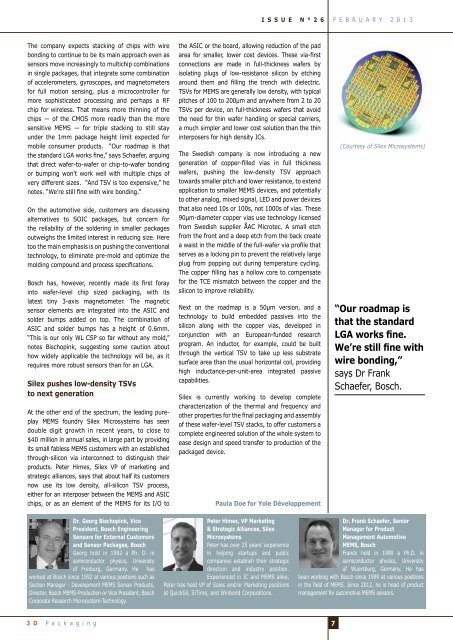
(Courtesy of Silex Microsystems)<br />
“Our roadmap is<br />
that the standard<br />
LGA works fine.<br />
We’re still fine with<br />
wire bonding,”<br />
says Dr Frank<br />
Schaefer, Bosch.<br />
Dr. Georg Bischopink, Vice<br />
President, Bosch Engineering<br />
Sensors for External Cus<strong>to</strong>mers<br />
and Sensor Packages, Bosch<br />
Georg hold in 1992 a Ph. D. in<br />
semiconduc<strong>to</strong>r physics, University<br />
of Freiburg, Germany. He has<br />
worked at Bosch since 1992 at various positions such as<br />
Section Manager - Development <strong>MEMS</strong> Sensor Products,<br />
Direc<strong>to</strong>r, Bosch <strong>MEMS</strong>-Production or Vice President, Bosch<br />
Corporate Research Microsystem-Technology.<br />
Peter Himes, VP Marketing<br />
& Strategic Alliances, Silex<br />
Microsystems<br />
Peter has over 25 years’ experience<br />
in helping startups and public<br />
companies establish their strategic<br />
direction and industry position.<br />
Experienced in IC and <strong>MEMS</strong> alike,<br />
Peter has held VP of Sales and/or Marketing positions<br />
at QuickSil, SiTime, and Winbond Corporations.<br />
Dr. Frank Schaefer, Senior<br />
Manager for Product<br />
Management Au<strong>to</strong>motive<br />
<strong>MEMS</strong>, Bosch<br />
Franck hold in 1999 a Ph.D. in<br />
semiconduc<strong>to</strong>r physics, University<br />
of Wuerzburg, Germany. He has<br />
been working with Bosch since 1999 at various positions<br />
in the field of <strong>MEMS</strong>. Since 2012, he is head of product<br />
management for au<strong>to</strong>motive <strong>MEMS</strong> sensors.<br />
3 D P a c k a g i n g<br />
7


