

Two very different approaches to MEMS packaging - I-Micronews
Two very different approaches to MEMS packaging - I-Micronews
Two very different approaches to MEMS packaging - I-Micronews

Create successful ePaper yourself
Turn your PDF publications into a flip-book with our unique Google optimized e-Paper software.
F e b r u a r y 2 0 1 3 I S S U E N ° 2 6<br />
“Instead of putting<br />
the high value<br />
ASIC on a blank<br />
silicon interposer<br />
with vias and<br />
interconnects,<br />
we could put the<br />
pho<strong>to</strong>nics on the<br />
interposer and<br />
connect it directly<br />
<strong>to</strong> the upstairs<br />
die,” says Chris<br />
Bergey, Luxtera.<br />
INDUSTRY REVIEW – FOCUS ON SILICON PHOTONICS PACKAGING<br />
Silicon pho<strong>to</strong>nics looks for 2.5D<br />
assembly at OSATs<br />
Though silicon pho<strong>to</strong>nics has so far relied on one-chip integration of optics with<br />
electronics <strong>to</strong> start <strong>to</strong> get real traction in the data communications market, sec<strong>to</strong>r<br />
pioneer Luxtera sees the evolving <strong>packaging</strong> technology for heterogeneous 2.5D<br />
integration as the next generation solution <strong>to</strong> scale integrated pho<strong>to</strong>nics <strong>to</strong> high<br />
volume production. The company is working <strong>to</strong> build up a scalable back end silicon<br />
pho<strong>to</strong>nics infrastructure with OSATs and assembly and test <strong>to</strong>ol suppliers.<br />
Silicon pho<strong>to</strong>nics is still a small emerging<br />
market, but growing demand for high speed<br />
data communication is starting <strong>to</strong> spur serious<br />
interest. Yole Développement sees silicon pho<strong>to</strong>nic<br />
systems sales of some $215 million by 2017. The<br />
sec<strong>to</strong>r got a recent boost when Facebook announced<br />
plans <strong>to</strong> move <strong>to</strong> silicon pho<strong>to</strong>nics for its server<br />
interconnect, <strong>to</strong> enable disaggregation of computing<br />
in<strong>to</strong> separate units for more efficient sharing of<br />
memory among multiple processors. Leading supplier<br />
Luxtera says it has shipped more than half a million of<br />
the optics-and-transis<strong>to</strong>rs-on-silicon devices <strong>to</strong> date,<br />
primarily for active optical cables in data centers, and<br />
sees demand for >10M units a year by 2016.<br />
One key enabler of this growth will be moving from<br />
the electrical system-on-a-chip approach <strong>to</strong> an<br />
electrical and optical system in a package solution,<br />
made possible by the recent advances in 3D<br />
<strong>packaging</strong> technology. “The silicon infrastructure’s<br />
development of 2.5D heterogeneous integration is a<br />
key technology path forward for pho<strong>to</strong>nics,” says Chris<br />
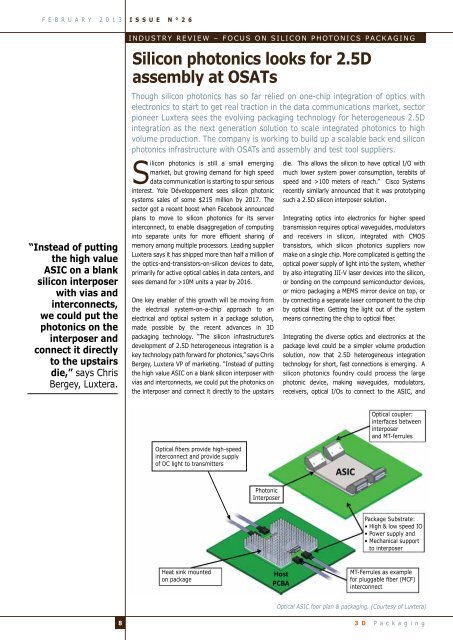
Bergey, Luxtera VP of marketing. “Instead of putting<br />
the high value ASIC on a blank silicon interposer with<br />
vias and interconnects, we could put the pho<strong>to</strong>nics on<br />
the interposer and connect it directly <strong>to</strong> the upstairs<br />
die. This allows the silicon <strong>to</strong> have optical I/O with<br />
much lower system power consumption, terabits of<br />
speed and >100 meters of reach.” Cisco Systems<br />
recently similarly announced that it was pro<strong>to</strong>typing<br />
such a 2.5D silicon interposer solution.<br />
Integrating optics in<strong>to</strong> electronics for higher speed<br />
transmission requires optical waveguides, modula<strong>to</strong>rs<br />
and receivers in silicon, integrated with CMOS<br />
transis<strong>to</strong>rs, which silicon pho<strong>to</strong>nics suppliers now<br />
make on a single chip. More complicated is getting the<br />
optical power supply of light in<strong>to</strong> the system, whether<br />
by also integrating III-V laser devices in<strong>to</strong> the silicon,<br />
or bonding on the compound semiconduc<strong>to</strong>r devices,<br />
or micro <strong>packaging</strong> a <strong>MEMS</strong> mirror device on <strong>to</strong>p, or<br />
by connecting a separate laser component <strong>to</strong> the chip<br />
by optical fiber. Getting the light out of the system<br />
means connecting the chip <strong>to</strong> optical fiber.<br />
Integrating the diverse optics and electronics at the<br />
package level could be a simpler volume production<br />
solution, now that 2.5D heterogeneous integration<br />
technology for short, fast connections is emerging. A<br />
silicon pho<strong>to</strong>nics foundry could process the large<br />
pho<strong>to</strong>nic device, making waveguides, modula<strong>to</strong>rs,<br />
receivers, optical I/Os <strong>to</strong> connect <strong>to</strong> the ASIC, and<br />
Optical coupler:<br />
interfaces between<br />
interposer<br />
and MT-ferrules<br />
Optical fibers provide high-speed<br />
interconnect and provide supply<br />
of DC light <strong>to</strong> transmitters<br />
Pho<strong>to</strong>nic<br />
Interposer<br />
Package Substrate:<br />
• High & low speed IO<br />
• Power supply and<br />
• Mechanical support<br />
<strong>to</strong> interposer<br />
Heat sink mounted<br />
on package<br />
MT-Ferrules as example<br />
for pluggable fiber (MCF)<br />
interconnect<br />
Optical ASIC foor plan & <strong>packaging</strong>. (Courtesy of Luxtera)<br />
8<br />
3 D P a c k a g i n g


