

3M & SUSS announce agreement on temporary wafer ... - I-Micronews
3M & SUSS announce agreement on temporary wafer ... - I-Micronews
3M & SUSS announce agreement on temporary wafer ... - I-Micronews

You also want an ePaper? Increase the reach of your titles
YUMPU automatically turns print PDFs into web optimized ePapers that Google loves.
J U L Y 2 0 0 9 i s s u e n ° 1 1<br />
N e w s l e t t e r o n 3 D I C , T S V , W L P & E m b e d d e d T e c h n o l o g i e s<br />
C O M P A N Y P R O F I L E<br />
The <strong>wafer</strong> level camera Juggernaut Novel technology,<br />
supply chain innovati<strong>on</strong> and commercial pressures<br />
drive rapid adopti<strong>on</strong><br />
Wafer level cameras represent a tantalising opportunity to substantially decrease the cost and form factor of solid state<br />
camera modules. After many years of endeavour, successful integrati<strong>on</strong> of the technologies necessary to manufacture<br />
true <strong>wafer</strong> level cameras was <str<strong>on</strong>g>announce</str<strong>on</strong>g>d in 2007. While there is great potential for these cameras <strong>on</strong> mobile platforms,<br />
OEMs are reluctant to design-in product that is not commercially available and camera module manufacturers will not<br />
invest in the necessary manufacturing facilities when there is no demand. This article discuses the technical, supply chain<br />
and commercial challenges of <strong>wafer</strong> level camera technology and explains the background behind analysts predicti<strong>on</strong> that<br />
by 2012 reflowable <strong>wafer</strong> level cameras will account for 30% of the 2bn camera modules manufactured annually. For Yole<br />
Développement, Giles Humpst<strong>on</strong> & Bents Kidr<strong>on</strong> from Tessera has highlighted what the trends, markets and challenges<br />
for WLC are.<br />
Yole Développement: Could you define<br />
what a <strong>wafer</strong> level camera is?<br />
Giles Humpst<strong>on</strong> & Bents Kidr<strong>on</strong>: Wafer level<br />
camera is “<strong>wafer</strong> level manufacture of all parts of a<br />
solid state camera that are then combined at the<br />
<strong>wafer</strong> level”. The final step of manufacture is <strong>wafer</strong><br />
dicing, which frees complete and individual camera<br />
modules. Recently the technical issues to make<br />
<strong>wafer</strong> level cameras have all been solved and<br />
product <str<strong>on</strong>g>announce</str<strong>on</strong>g>ments appeared in 2007.<br />
However these first generati<strong>on</strong> <strong>wafer</strong> level cameras<br />
are not manufactured according to the methodology<br />
suggested by the definiti<strong>on</strong> above. This is because it<br />
is perceived as unec<strong>on</strong>omic to do so. The issue is<br />
that the optical area of an imager die is very much<br />
smaller than the die area because of the other<br />
electr<strong>on</strong>ics each chip c<strong>on</strong>tains. The result is a<br />
mismatch in populati<strong>on</strong> between the lens <strong>wafer</strong>s and<br />
the semic<strong>on</strong>ductor <strong>wafer</strong>s; a 200m diameter lens<br />
<strong>wafer</strong> being able to accommodate about 4 times as<br />
many lenses as an imager <strong>wafer</strong> c<strong>on</strong>taining VGA<br />
resoluti<strong>on</strong> die. There is also the issue of compound<br />
yield when mating a stack of optical comp<strong>on</strong>ents<br />
fabricated at the <strong>wafer</strong> level with a <strong>wafer</strong> c<strong>on</strong>taining<br />
imager die. In both cases the number of good optical<br />
die is less than the total number of die.<br />
C<strong>on</strong>sequently it is ec<strong>on</strong>omically more favourable to<br />
make the optical train at the <strong>wafer</strong> level, dice it into<br />
individual optical stacks then c<strong>on</strong>duct die-to-<strong>wafer</strong><br />
assembly to build camera modules. Dicing the<br />
populated semic<strong>on</strong>ductor <strong>wafer</strong> yields completed<br />
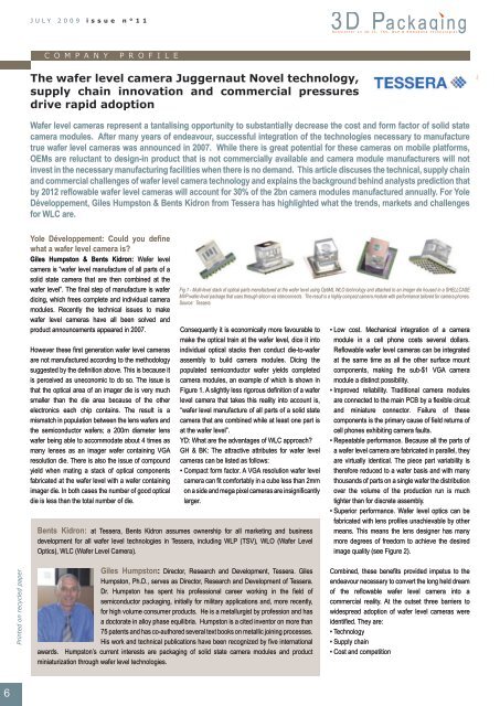
camera modules, an example of which is shown in<br />
Figure 1. A slightly less rigorous definiti<strong>on</strong> of a <strong>wafer</strong><br />
level camera that takes this reality into account is,<br />
“<strong>wafer</strong> level manufacture of all parts of a solid state<br />
camera that are combined while at least <strong>on</strong>e part is<br />
at the <strong>wafer</strong> level”.<br />
YD: What are the advantages of WLC approach?<br />
GH & BK: The attractive attributes for <strong>wafer</strong> level<br />
cameras can be listed as follows:<br />
• Compact form factor. A VGA resoluti<strong>on</strong> <strong>wafer</strong> level<br />
camera can fit comfortably in a cube less than 2mm<br />
<strong>on</strong> a side and mega pixel cameras are insignificantly<br />
larger.<br />
Bents Kidr<strong>on</strong>: at Tessera, Bents Kidr<strong>on</strong> assumes ownership for all marketing and business<br />
development for all <strong>wafer</strong> level technologies in Tessera, including WLP (TSV), WLO (Wafer Level<br />
Optics), WLC (Wafer Level Camera).<br />
Fig 1 - Multi-level stack of optical parts manufactured at the <strong>wafer</strong> level using OptiML WLO technology and attached to an imager die housed in a SHELLCASE<br />
MVP <strong>wafer</strong>-level package that uses through silic<strong>on</strong> via interc<strong>on</strong>nects. The result is a highly compact camera module with performance tailored for camera ph<strong>on</strong>es.<br />
Source: Tessera.<br />
• Low cost. Mechanical integrati<strong>on</strong> of a camera<br />
module in a cell ph<strong>on</strong>e costs several dollars.<br />
Reflowable <strong>wafer</strong> level cameras can be integrated<br />
at the same time as all the other surface mount<br />
comp<strong>on</strong>ents, making the sub-$1 VGA camera<br />
module a distinct possibility.<br />
• Improved reliability. Traditi<strong>on</strong>al camera modules<br />
are c<strong>on</strong>nected to the main PCB by a flexible circuit<br />
and miniature c<strong>on</strong>nector. Failure of these<br />
comp<strong>on</strong>ents is the primary cause of field returns of<br />
cell ph<strong>on</strong>es exhibiting camera faults.<br />
• Repeatable performance. Because all the parts of<br />
a <strong>wafer</strong> level camera are fabricated in parallel, they<br />
are virtually identical. The piece part variability is<br />
therefore reduced to a <strong>wafer</strong> basis and with many<br />
thousands of parts <strong>on</strong> a single <strong>wafer</strong> the distributi<strong>on</strong><br />
over the volume of the producti<strong>on</strong> run is much<br />
tighter than for discrete assembly.<br />
• Superior performance. Wafer level optics can be<br />
fabricated with lens profiles unachievable by other<br />
means. This means the lens designer has many<br />
more degrees of freedom to achieve the desired<br />
image quality (see Figure 2).<br />
Printed <strong>on</strong> recycled paper<br />
Giles Humpst<strong>on</strong>: Director, Research and Development, Tessera. Giles<br />
Humpst<strong>on</strong>, Ph.D., serves as Director, Research and Development of Tessera.<br />
Dr. Humpst<strong>on</strong> has spent his professi<strong>on</strong>al career working in the field of<br />
semic<strong>on</strong>ductor packaging, initially for military applicati<strong>on</strong>s and, more recently,<br />
for high volume c<strong>on</strong>sumer products. He is a metallurgist by professi<strong>on</strong> and has<br />
a doctorate in alloy phase equilibria. Humpst<strong>on</strong> is a cited inventor <strong>on</strong> more than<br />
75 patents and has co-authored several text books <strong>on</strong> metallic joining processes.<br />
His work and technical publicati<strong>on</strong>s have been recognized by five internati<strong>on</strong>al<br />
awards. Humpst<strong>on</strong>’s current interests are packaging of solid state camera modules and product<br />
miniaturizati<strong>on</strong> through <strong>wafer</strong> level technologies.<br />
Combined, these benefits provided impetus to the<br />
endeavour necessary to c<strong>on</strong>vert the l<strong>on</strong>g held dream<br />
of the reflowable <strong>wafer</strong> level camera into a<br />
commercial reality. At the outset three barriers to<br />
widespread adopti<strong>on</strong> of <strong>wafer</strong> level cameras were<br />
identified. They are:<br />
• Technology<br />
• Supply chain<br />
• Cost and competiti<strong>on</strong><br />
6


