

3M & SUSS announce agreement on temporary wafer ... - I-Micronews
3M & SUSS announce agreement on temporary wafer ... - I-Micronews
3M & SUSS announce agreement on temporary wafer ... - I-Micronews

You also want an ePaper? Increase the reach of your titles
YUMPU automatically turns print PDFs into web optimized ePapers that Google loves.
J U L Y 2 0 0 9 i s s u e n ° 1 1<br />
N e w s l e t t e r o n 3 D I C , T S V , W L P & E m b e d d e d T e c h n o l o g i e s<br />
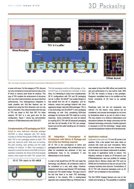
Fig2 - From design to packaging: dem<strong>on</strong>strati<strong>on</strong> achieved between STMicroelectr<strong>on</strong>ics and CEA-LETI<br />
or even a bit more. For this category of TSV, dice are<br />
not <strong>on</strong>ly c<strong>on</strong>nected at b<strong>on</strong>d pad level but also at the<br />
IP block or memory bank levels for instance. This<br />
type of TSV enables the achievement of structures<br />
with very short interc<strong>on</strong>necti<strong>on</strong>s and good electrical<br />
performances. True heterogeneous integrati<strong>on</strong> is<br />
made possible and SoC–like features can be<br />
realized but using the third dimensi<strong>on</strong> and not <strong>on</strong>ly<br />
the x-y directi<strong>on</strong>s. Dice interc<strong>on</strong>nected with this type<br />
of TSV are closer to SoC than SiP. For these<br />
reas<strong>on</strong>s, 3D SoC is a very good term for this<br />
c<strong>on</strong>figurati<strong>on</strong>. Figure 1 shows key dem<strong>on</strong>strati<strong>on</strong><br />
achieve in STMicroelectr<strong>on</strong>ics with CEA-LETI.<br />
Complementarity of 3D packaging and 3D IC<br />
Except for some <strong>wafer</strong>-level chip-scale packages<br />
(WLCSP) or silic<strong>on</strong> interposer with TSV directly<br />
mounted <strong>on</strong> Printed Wiring Board (PWB) with a BGA<br />
balls, TSV is not a packaging soluti<strong>on</strong> by itself. TSV<br />
uses <strong>on</strong>ly “back-end world” skills such as b<strong>on</strong>ding,<br />
fine pitch bumping, back grinding and thin <strong>wafer</strong><br />
handling, for instance. In effect, final packaging is<br />
required to c<strong>on</strong>nect the device to the PWB. And due to<br />
assembly c<strong>on</strong>straints, the choice of the final package<br />
soluti<strong>on</strong> could impact the entire TSV process flow.<br />
Fig3 - 3D IC TSV stack in 3D-eWLB (Courtesy of ST-Ericss<strong>on</strong>)<br />
This final packaging could be a BGA package, a Fan-<br />
Out WLP type, an embedded die in laminate, or other.<br />
Here, it is interesting to notice how complementary<br />
3D IC c<strong>on</strong>figurati<strong>on</strong>s with TSV and 3D packaging<br />
can be. In effect, 3D eWLB TM can enable designs to<br />
fully benefit from the 3D IC integrati<strong>on</strong>, and for<br />
instance, reduce the package footprint with more<br />
aggressive design rules than BGA packages. TSV is<br />
a new technology and 3D eWLB TM a new packaging<br />
technology as well. Only c<strong>on</strong>sidering BGA-type<br />
packages for structures with TSV might be a wr<strong>on</strong>g<br />
reas<strong>on</strong>ing. Some c<strong>on</strong>straints can even be relaxed<br />
by coupling 3D IC TSV with 3D advanced packaging<br />
and then the full benefits of the TSV can emerge.<br />
Issues such as thin <strong>wafer</strong> handling can, for instance,<br />
be simplified.<br />
3D Integrati<strong>on</strong>: C<strong>on</strong>vergence of<br />
Architecture with Silic<strong>on</strong> & Package and<br />
Out of the box thinking required.<br />
3D IC TSV is the c<strong>on</strong>vergence of silic<strong>on</strong> and<br />
packaging with the design. New architectures can in<br />
effect be c<strong>on</strong>sidered and achieved. In fact, new<br />
architectures have to be c<strong>on</strong>sidered if cost<br />
effectiveness is to be reached.<br />
In order to fully benefit from 3D TSV and make this<br />
technology cost effective, 3D architecture needs to<br />
be c<strong>on</strong>sidered at a very early stage. However,<br />
designers are facing a gap between TSV technology<br />
process and TSV system design. This gap is due to<br />
the fact that there is no clear TSV technology<br />
roadmap in the industry. With a scaling-based<br />
approach and a classical follow-up of Moore’s law, it<br />
was easier to focus the R&D efforts and predict the<br />
size and performance of a new techno node. With<br />
3D TSV, the industry is facing a new paradigm.<br />
Designers’ mentalities have to be modified and the<br />
former c<strong>on</strong>straints of 2D have to be partially<br />
forgotten.<br />
Roadmaps exist, but are not necessarily very<br />
relevant. For this reas<strong>on</strong>, many opti<strong>on</strong>s can be<br />
c<strong>on</strong>sidered, and process technologists do not know<br />
by themselves where to go and <strong>on</strong> what to focus.<br />
The <strong>on</strong>ly soluti<strong>on</strong> is to reinforce collaborati<strong>on</strong>s and<br />
discussi<strong>on</strong>s between the design community and the<br />
hardware technology community. A holistic approach<br />
is necessary to find the technology / design sweet<br />
spot and the applicati<strong>on</strong> needs to drive developments.<br />
Applicati<strong>on</strong> roadmap<br />
Applicati<strong>on</strong>s that could use TSV and 3D remain a hot<br />
questi<strong>on</strong>. Only a few people have clear views <strong>on</strong><br />
products that could use such innovati<strong>on</strong>s. Many<br />
niche markets would exist, for sure. However, when<br />
we think about core chipset comp<strong>on</strong>ents in wireless,<br />
the scope of applicati<strong>on</strong>s tends to reduce. The<br />
following roadmap is based <strong>on</strong> ST-Ericss<strong>on</strong>’s and<br />
STMicroelectr<strong>on</strong>ics’ view and portfolio for wireless<br />
products (fig 2). Memory stacks with TSV such as<br />
DRAM are not menti<strong>on</strong>ed as they are not part of the<br />
company business area anymore. Combinati<strong>on</strong>s of<br />
3D IC TSV with advanced packaging such as 3D<br />
eWLB TM are not detailed <strong>on</strong> the schematics.<br />
The first CMOS Imaging Sensors are now <strong>on</strong> the<br />
market and ramping up. The possibility to substitute<br />
Printed <strong>on</strong> recycled paper<br />
3


