

Embedded Die - I-Micronews
Embedded Die - I-Micronews
Embedded Die - I-Micronews

You also want an ePaper? Increase the reach of your titles
YUMPU automatically turns print PDFs into web optimized ePapers that Google loves.
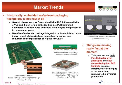
Market Trends<br />
• Historically, embedded wafer-level-packaging<br />
technology is not new at all<br />
– Several players such as Freescale with its RCP, Infineon with its<br />
eWLB and Ibiden for die embeddeding into PCB laminated<br />
substrates have developed dedicated technologies and process IP<br />
in this area for years.<br />
– Benefits of embedded package integration include miniaturization,<br />
improvement of electrical and thermal performance, cost<br />
reduction and simplification of logistic for OEMs<br />
1st generation eWLB cross-section<br />
(Courtesy of Infineon)<br />
Multi-chip SiP Module<br />
based on Chip Embedding technology<br />
(Courtesy of AT&S)<br />
<strong>Embedded</strong> die iBGA package<br />
(Courtesy of Imbera / Daeduck)<br />
Integrated passive IC “ready” for<br />
embedding into PCB laminate<br />
(Courtesy of NXP / FCI)<br />
• Things are moving<br />
really fast at the<br />
moment<br />
– This year, we see both<br />
Fan-Out wafer level<br />
packaging and chip<br />
embeddeding into PCB<br />
laminate package<br />
infrastructures emerging<br />
at the same time,<br />
ramping to high volume<br />
production<br />
© 2010 • 8<br />
Copyrights © Yole Développement SARL. All rights reserved.


