

Embedded Die - I-Micronews
Embedded Die - I-Micronews
Embedded Die - I-Micronews

You also want an ePaper? Increase the reach of your titles
YUMPU automatically turns print PDFs into web optimized ePapers that Google loves.
<strong>Embedded</strong> die package technology<br />
to expand fast from niche to high volume markets<br />
• At the same time, embedded die package technology has made a lot of progress on its side !<br />
– Based on PCB laminate infrastructure, chip embeddeding technology is actually on the way to catch a<br />
relatively important portion of the actual „Fan-in‟ WLCSP packaging business as it does leverage the<br />
existing WLP/RDL infrastructure already established worldwide: indeed, most of WLCSP die applications are<br />
“embedded ready”, so to realize the full benefits of this “WLCSP to <strong>Embedded</strong> die” conversion, only a few<br />
extra manufacturing steps are missing like the realization of thin copper plating process, extreme wafer<br />
thinning down to 50μm, thin dies handling and dicing.<br />
© 2010 • 12<br />
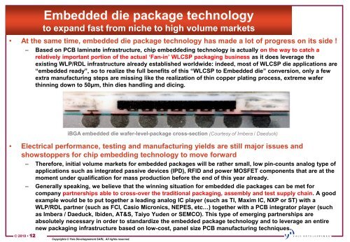
iBGA embedded die wafer-level-package cross-section (Courtesy of Imbera / Daeduck)<br />
• Electrical performance, testing and manufacturing yields are still major issues and<br />
showstoppers for chip embedding technology to move forward<br />
– Therefore, initial volume markets for embedded packages will be rather small, low pin-counts analog type of<br />
applications such as integrated passive devices (IPD), RFID and power MOSFET components that are at the<br />
moment under qualification for mass production before the end of this year already.<br />
– Generally speaking, we believe that the winning situation for embedded die packages can be met for<br />
company partnerships able to cross-over the traditional packaging, assembly and test supply chain. A good<br />
example would be to put together a leading analog IC player (such as TI, Maxim IC, NXP or ST) with a<br />
WLP/RDL partner (such as FCI, Casio Micronics, NEPES, etc…) together with a PCB integrator player (such<br />
as Imbera / Daeduck, Ibiden, AT&S, Taiyo Yuden or SEMCO). This type of emerging partnerships are<br />
absolutely necessary in order to standardize the embedded package technology and to leverage an entire<br />
new packaging infrastructure based on low-cost, panel size PCB manufacturing techniques.<br />
Copyrights © Yole Développement SARL. All rights reserved.


