

Fan-in WLCSP matures, what's next? IMT on the role ... - I-Micronews
Fan-in WLCSP matures, what's next? IMT on the role ... - I-Micronews
Fan-in WLCSP matures, what's next? IMT on the role ... - I-Micronews

You also want an ePaper? Increase the reach of your titles
YUMPU automatically turns print PDFs into web optimized ePapers that Google loves.
F E B R U A R Y 2 0 1 0 i s s u e n ° 1 4<br />
N e w s l e t t e r o n 3 D I C , T S V , W L P & E m b e d d e d T e c h n o l o g i e s<br />
C O M P A N Y V I S I O N<br />
<str<strong>on</strong>g>IMT</str<strong>on</strong>g> <strong>on</strong> <strong>the</strong> <strong>role</strong> of Wafer-Level Packag<str<strong>on</strong>g>in</str<strong>on</strong>g>g <str<strong>on</strong>g>in</str<strong>on</strong>g> MEMS<br />
From page 1<br />
In <strong>the</strong> future, WLP will play a greater <strong>role</strong> <str<strong>on</strong>g>in</str<strong>on</strong>g> <strong>the</strong><br />
<str<strong>on</strong>g>in</str<strong>on</strong>g>tegrati<strong>on</strong> of heterogeneous technologies. Right<br />
now, we’re see<str<strong>on</strong>g>in</str<strong>on</strong>g>g die-level MEMS and CMOS<br />
devices wire b<strong>on</strong>ded and encapsulated. We also see<br />
build<str<strong>on</strong>g>in</str<strong>on</strong>g>g MEMS directly <strong>on</strong> CMOS wafers. Not too<br />
far off, we expect to see completed MEMS wafers<br />
or wafer stacks b<strong>on</strong>ded to completed CMOS wafers.<br />
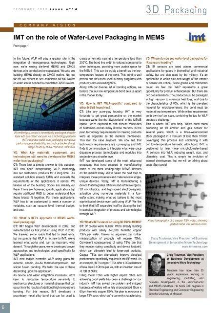
IR emitter/gas sensor is hermetically packaged at wafer<br />
level with sub-mTorr vacuum. As a technology platform<br />
<str<strong>on</strong>g>IMT</str<strong>on</strong>g> <str<strong>on</strong>g>in</str<strong>on</strong>g>tegrates wafer-level packag<str<strong>on</strong>g>in</str<strong>on</strong>g>g to improve<br />
performance and reliability, and reduce backend cost.<br />
Image courtesy of ICx Precisi<strong>on</strong> Phot<strong>on</strong>ics.<br />
YD: What key materials, equipment, and<br />
technologies still need to developed for MEMS<br />
wafer-level packag<str<strong>on</strong>g>in</str<strong>on</strong>g>g?<br />
CT: There isn’t a simple answer to this questi<strong>on</strong>.<br />
<str<strong>on</strong>g>IMT</str<strong>on</strong>g> has been <str<strong>on</strong>g>in</str<strong>on</strong>g>corporat<str<strong>on</strong>g>in</str<strong>on</strong>g>g WLP technology<br />
<str<strong>on</strong>g>in</str<strong>on</strong>g>to our customers’ products for a l<strong>on</strong>g time. Our<br />
standard soluti<strong>on</strong> already fulfills and exceeds <strong>the</strong><br />
requirements of <strong>the</strong> applicati<strong>on</strong>s it serves. We<br />
believe all of <strong>the</strong> build<str<strong>on</strong>g>in</str<strong>on</strong>g>g blocks are already out<br />
<strong>the</strong>re. There are, however, specific applicati<strong>on</strong>s that<br />
require additi<strong>on</strong>al R&D to better understand how<br />
those blocks fit toge<strong>the</strong>r. For those applicati<strong>on</strong>s,<br />
WLP has to be customized to meet a number of<br />
variables, such as vacuum level, <strong>the</strong>rmal budget,<br />
and cost.<br />
YD: What is <str<strong>on</strong>g>IMT</str<strong>on</strong>g>’s approach to MEMS waferlevel<br />
packag<str<strong>on</strong>g>in</str<strong>on</strong>g>g?<br />
CT: <str<strong>on</strong>g>IMT</str<strong>on</strong>g> began WLP development <str<strong>on</strong>g>in</str<strong>on</strong>g> 2002, and<br />
manufactured its first product us<str<strong>on</strong>g>in</str<strong>on</strong>g>g WLP <str<strong>on</strong>g>in</str<strong>on</strong>g> 2003.<br />
We traveled some roads that led to dead ends,<br />
but my po<str<strong>on</strong>g>in</str<strong>on</strong>g>t is that WLP is not new to <str<strong>on</strong>g>IMT</str<strong>on</strong>g>. We’ve<br />
learned what works and, just as important, what<br />
doesn’t. Through <strong>the</strong> years, we’ve developed proven<br />
approaches and technologies used specifically for<br />
WLP applicati<strong>on</strong>s.<br />
<str<strong>on</strong>g>IMT</str<strong>on</strong>g> now makes hermetic WLP us<str<strong>on</strong>g>in</str<strong>on</strong>g>g glass frit,<br />
eutectic, anodic, Au-Au <strong>the</strong>rmocompressi<strong>on</strong>, and<br />
silic<strong>on</strong> fusi<strong>on</strong> b<strong>on</strong>d<str<strong>on</strong>g>in</str<strong>on</strong>g>g. We tailor <strong>the</strong> use of <strong>the</strong>se<br />
depend<str<strong>on</strong>g>in</str<strong>on</strong>g>g up<strong>on</strong> <strong>the</strong> applicati<strong>on</strong>.<br />
As device and wafer <str<strong>on</strong>g>in</str<strong>on</strong>g>tegrati<strong>on</strong> <str<strong>on</strong>g>in</str<strong>on</strong>g>creases, we’re<br />
keen to recognize temperature sensitivity to<br />
mechanical structures or material stresses that can<br />
occur from <strong>the</strong> results of additi<strong>on</strong>al high-temperature<br />
b<strong>on</strong>d<str<strong>on</strong>g>in</str<strong>on</strong>g>g. For this reas<strong>on</strong>, <str<strong>on</strong>g>IMT</str<strong>on</strong>g> developed a<br />
proprietary metal alloy b<strong>on</strong>d that can be used to<br />
create a hermetic seal at a temperature less than<br />
200°C. The b<strong>on</strong>d l<str<strong>on</strong>g>in</str<strong>on</strong>g>e width is reduced compared to<br />
o<strong>the</strong>r techniques, provid<str<strong>on</strong>g>in</str<strong>on</strong>g>g more usable space for<br />
<strong>the</strong> MEMS. This can be as big a benefit as <strong>the</strong> lowtemperature<br />
feature of <strong>the</strong> b<strong>on</strong>d. This b<strong>on</strong>d is well<br />
proven and has been used <str<strong>on</strong>g>in</str<strong>on</strong>g> many programs with<br />
product yields exceed<str<strong>on</strong>g>in</str<strong>on</strong>g>g 99%.<br />
Al<strong>on</strong>g with our diverse list of b<strong>on</strong>d<str<strong>on</strong>g>in</str<strong>on</strong>g>g opti<strong>on</strong>s, we<br />
believe that our low-temperature b<strong>on</strong>d sets us apart<br />
<str<strong>on</strong>g>in</str<strong>on</strong>g> <strong>the</strong> market today.<br />
YD: How is <str<strong>on</strong>g>IMT</str<strong>on</strong>g> ‘WLP-specific’ compared to<br />
o<strong>the</strong>r MEMS foundries?<br />
CT: Like any pure-play foundry, <str<strong>on</strong>g>IMT</str<strong>on</strong>g> is very<br />
fortunate to get great perspective <strong>on</strong> <strong>the</strong> market<br />
because we’re like <strong>the</strong> ‘Switzerland’ of <strong>the</strong> MEMS<br />
space—we’re exposed to and service multitudes<br />
of customers across many diverse markets. In <strong>the</strong><br />
past, technology requirements for creat<str<strong>on</strong>g>in</str<strong>on</strong>g>g products<br />
were as separate as <strong>the</strong> markets <strong>the</strong>mselves.<br />
This isn’t <strong>the</strong> case anymore. We now see that<br />
technology requirements are c<strong>on</strong>verg<str<strong>on</strong>g>in</str<strong>on</strong>g>g and <str<strong>on</strong>g>IMT</str<strong>on</strong>g><br />
f<str<strong>on</strong>g>in</str<strong>on</strong>g>ds it comm<strong>on</strong>place to <str<strong>on</strong>g>in</str<strong>on</strong>g>tegrate what were <strong>on</strong>ce<br />
disparate process technologies and modules <str<strong>on</strong>g>in</str<strong>on</strong>g>to<br />
s<str<strong>on</strong>g>in</str<strong>on</strong>g>gle devices at wafer level.<br />
<str<strong>on</strong>g>IMT</str<strong>on</strong>g> has developed some of <strong>the</strong> most advanced<br />
processes that have resulted <str<strong>on</strong>g>in</str<strong>on</strong>g> manufactur<str<strong>on</strong>g>in</str<strong>on</strong>g>g<br />
some of <strong>the</strong> most lead<str<strong>on</strong>g>in</str<strong>on</strong>g>g-edge MEMS devices<br />
<strong>on</strong> <strong>the</strong> market today. We’ve taken <strong>the</strong> <str<strong>on</strong>g>next</str<strong>on</strong>g> step to<br />
<str<strong>on</strong>g>in</str<strong>on</strong>g>tegrate <strong>the</strong>se processes and materials <str<strong>on</strong>g>in</str<strong>on</strong>g>to s<str<strong>on</strong>g>in</str<strong>on</strong>g>gle,<br />
unique devices. Today, <str<strong>on</strong>g>IMT</str<strong>on</strong>g> is manufactur<str<strong>on</strong>g>in</str<strong>on</strong>g>g a<br />
device that <str<strong>on</strong>g>in</str<strong>on</strong>g>tegrates reflexive and refractive optics,<br />
3D microfluidics, and high-speed electromagnetic<br />
actuati<strong>on</strong> us<str<strong>on</strong>g>in</str<strong>on</strong>g>g numerous materials <str<strong>on</strong>g>in</str<strong>on</strong>g> a fourwafer<br />
stack, mak<str<strong>on</strong>g>in</str<strong>on</strong>g>g what we believe is <strong>the</strong> most<br />
sophisticated device ever built us<str<strong>on</strong>g>in</str<strong>on</strong>g>g WLP. We like<br />
to th<str<strong>on</strong>g>in</str<strong>on</strong>g>k that <str<strong>on</strong>g>IMT</str<strong>on</strong>g> separates itself by blaz<str<strong>on</strong>g>in</str<strong>on</strong>g>g <strong>the</strong> trail<br />
<str<strong>on</strong>g>in</str<strong>on</strong>g> complex <str<strong>on</strong>g>in</str<strong>on</strong>g>tegrati<strong>on</strong> of process and technologies<br />
through WLP.<br />
YD: What’s <str<strong>on</strong>g>IMT</str<strong>on</strong>g>’s stance <strong>on</strong> us<str<strong>on</strong>g>in</str<strong>on</strong>g>g 3D TSV <str<strong>on</strong>g>in</str<strong>on</strong>g> MEMS?<br />
CT: Of course we’re ‘bullish.’ We’re already build<str<strong>on</strong>g>in</str<strong>on</strong>g>g<br />
products with nearly 140,000 hermetic copper<br />
TSVs per wafer. There’s no argument that fur<strong>the</strong>r<br />
m<str<strong>on</strong>g>in</str<strong>on</strong>g>iaturizati<strong>on</strong> of products will require TSVs.<br />
C<strong>on</strong>venient c<strong>on</strong>sequences of us<str<strong>on</strong>g>in</str<strong>on</strong>g>g TSVs are that<br />
<strong>the</strong>y reduce rout<str<strong>on</strong>g>in</str<strong>on</strong>g>g complexity and device footpr<str<strong>on</strong>g>in</str<strong>on</strong>g>t,<br />
which can ultimately lead to lower-cost products.<br />
Copper TSVs can dramatically improve electrical<br />
performance-specifically required <str<strong>on</strong>g>in</str<strong>on</strong>g> <strong>the</strong> RF world. As<br />
an example, <str<strong>on</strong>g>IMT</str<strong>on</strong>g>’s copper TSVs offer a DC resistance<br />
of less than 0.1 Ohms per via, with an <str<strong>on</strong>g>in</str<strong>on</strong>g>serti<strong>on</strong> loss of<br />
-0.1dB at 6GHz.<br />
Fill<str<strong>on</strong>g>in</str<strong>on</strong>g>g metal TSVs with higher aspect ratios and<br />
achiev<str<strong>on</strong>g>in</str<strong>on</strong>g>g good yields has been a challenge for our<br />
<str<strong>on</strong>g>in</str<strong>on</strong>g>dustry. <str<strong>on</strong>g>IMT</str<strong>on</strong>g> has solved <strong>the</strong> problem and shipped<br />
hundreds of wafers with a fully characterized 15µm x<br />
60µm hermetic copper TSVs. We plan to announce a<br />
larger TSV so<strong>on</strong>, which we’re currently characteriz<str<strong>on</strong>g>in</str<strong>on</strong>g>g.<br />
YD: Where do you see wafer-level packag<str<strong>on</strong>g>in</str<strong>on</strong>g>g for<br />
IR sensors head<str<strong>on</strong>g>in</str<strong>on</strong>g>g?<br />
CT: IR sensors are used across commercial<br />
applicati<strong>on</strong>s for gases <str<strong>on</strong>g>in</str<strong>on</strong>g> biomedical and <str<strong>on</strong>g>in</str<strong>on</strong>g>dustrial<br />
safety, but are also used by <strong>the</strong> military. It’s an<br />
applicati<strong>on</strong> <str<strong>on</strong>g>in</str<strong>on</strong>g> which size and weight of <strong>the</strong> emitter<br />
or sensor are critical. S<str<strong>on</strong>g>in</str<strong>on</strong>g>ce grams and millimeters<br />
count, we feel that WLP represents a great<br />
opportunity for product enhancement. But <strong>the</strong>re are<br />
two c<strong>on</strong>siderati<strong>on</strong>s: The product must be packaged<br />
<str<strong>on</strong>g>in</str<strong>on</strong>g> high vacuum to m<str<strong>on</strong>g>in</str<strong>on</strong>g>imize heat loss; and due to<br />
<strong>the</strong> characteristics of VOx, which is <strong>the</strong> prevalent<br />
material for microbolometers, <strong>the</strong> b<strong>on</strong>d must be<br />
made at low temperature. While ei<strong>the</strong>r requirement<br />
<strong>on</strong> its own isn’t an issue, comb<str<strong>on</strong>g>in</str<strong>on</strong>g><str<strong>on</strong>g>in</str<strong>on</strong>g>g <strong>the</strong> two for WLP<br />
creates a challenge.<br />
This is where <str<strong>on</strong>g>IMT</str<strong>on</strong>g> can help. We’ve been mass<br />
produc<str<strong>on</strong>g>in</str<strong>on</strong>g>g an IR emitter and gas sensor for<br />
several years, which is a three-wafer-b<strong>on</strong>ded<br />
stack packaged <str<strong>on</strong>g>in</str<strong>on</strong>g> a vacuum of less than 1mTorr.<br />
Leverag<str<strong>on</strong>g>in</str<strong>on</strong>g>g this process and comb<str<strong>on</strong>g>in</str<strong>on</strong>g><str<strong>on</strong>g>in</str<strong>on</strong>g>g it with<br />
our low-temperature hermetic alloy b<strong>on</strong>d, <str<strong>on</strong>g>IMT</str<strong>on</strong>g> is<br />
positi<strong>on</strong>ed to help move microbolometer-based<br />
IR sensors <str<strong>on</strong>g>in</str<strong>on</strong>g>to WLP, reduc<str<strong>on</strong>g>in</str<strong>on</strong>g>g weight, size, and<br />
ultimately, cost. This is simply an evoluti<strong>on</strong> of<br />
<str<strong>on</strong>g>in</str<strong>on</strong>g>ternal development that we will be talk<str<strong>on</strong>g>in</str<strong>on</strong>g>g about<br />
so<strong>on</strong>. Stay tuned!<br />
X-ray tomography of a copper TSV wafer, show<str<strong>on</strong>g>in</str<strong>on</strong>g>g<br />
plated metal vias without voids.<br />
Craig Trautman, Vice President of Bus<str<strong>on</strong>g>in</str<strong>on</strong>g>ess<br />
Development at Innovative Micro Technology<br />
www.imtmems.com<br />
Craig Trautman, Vice President<br />
of Bus<str<strong>on</strong>g>in</str<strong>on</strong>g>ess Development at<br />
Innovative Micro Technology<br />
Trautman has more than 25<br />
years’ experience work<str<strong>on</strong>g>in</str<strong>on</strong>g>g <str<strong>on</strong>g>in</str<strong>on</strong>g><br />
eng<str<strong>on</strong>g>in</str<strong>on</strong>g>eer<str<strong>on</strong>g>in</str<strong>on</strong>g>g, market<str<strong>on</strong>g>in</str<strong>on</strong>g>g, and<br />
bus<str<strong>on</strong>g>in</str<strong>on</strong>g>ess development <str<strong>on</strong>g>in</str<strong>on</strong>g> <strong>the</strong> semic<strong>on</strong>ductor<br />
and MEMS <str<strong>on</strong>g>in</str<strong>on</strong>g>dustries. He holds B.S. degrees <str<strong>on</strong>g>in</str<strong>on</strong>g><br />
Electrical Eng<str<strong>on</strong>g>in</str<strong>on</strong>g>eer<str<strong>on</strong>g>in</str<strong>on</strong>g>g and Computer Eng<str<strong>on</strong>g>in</str<strong>on</strong>g>eer<str<strong>on</strong>g>in</str<strong>on</strong>g>g<br />
from <strong>the</strong> University of Missouri.<br />
6


