

Fan-in WLCSP matures, what's next? IMT on the role ... - I-Micronews
Fan-in WLCSP matures, what's next? IMT on the role ... - I-Micronews
Fan-in WLCSP matures, what's next? IMT on the role ... - I-Micronews

You also want an ePaper? Increase the reach of your titles
YUMPU automatically turns print PDFs into web optimized ePapers that Google loves.
F E B R U A R Y 2 0 1 0 i s s u e n ° 1 4<br />
N e w s l e t t e r o n 3 D I C , T S V , W L P & E m b e d d e d T e c h n o l o g i e s<br />
C O M P A N Y V I S I O N<br />
Packag<str<strong>on</strong>g>in</str<strong>on</strong>g>g challenges <str<strong>on</strong>g>in</str<strong>on</strong>g> high performance comput<str<strong>on</strong>g>in</str<strong>on</strong>g>g<br />
Over <strong>the</strong> past half century, <strong>the</strong> semic<strong>on</strong>ductor <str<strong>on</strong>g>in</str<strong>on</strong>g>dustry has been at <strong>the</strong> forefr<strong>on</strong>t of technological progress as dem<strong>on</strong>strated<br />
by its own products and what <strong>the</strong>y have made possible. The ma<str<strong>on</strong>g>in</str<strong>on</strong>g> areas of improvement <str<strong>on</strong>g>in</str<strong>on</strong>g>clude functi<strong>on</strong>ality per unit<br />
volume, speed of performance, power c<strong>on</strong>sumed per unit performance, cost per functi<strong>on</strong>, etc. The bulk of <strong>the</strong> credit goes<br />
to <strong>the</strong> m<str<strong>on</strong>g>in</str<strong>on</strong>g>iaturizati<strong>on</strong> and <str<strong>on</strong>g>in</str<strong>on</strong>g>tegrati<strong>on</strong> at <strong>the</strong> chip/wafer level as predicted by Moore’s Law, and made possible through<br />
advancements <str<strong>on</strong>g>in</str<strong>on</strong>g> manufactur<str<strong>on</strong>g>in</str<strong>on</strong>g>g, design, simulati<strong>on</strong> and materials.<br />
Even less than twenty years back, packag<str<strong>on</strong>g>in</str<strong>on</strong>g>g<br />
was c<strong>on</strong>sidered an afterthought by<br />
most of <strong>the</strong> <str<strong>on</strong>g>in</str<strong>on</strong>g>dustry, though <strong>the</strong> high<br />
performance comput<str<strong>on</strong>g>in</str<strong>on</strong>g>g segment was <strong>the</strong> first<br />
to devote significant resources for optimiz<str<strong>on</strong>g>in</str<strong>on</strong>g>g<br />
<strong>the</strong> package performance. Start<str<strong>on</strong>g>in</str<strong>on</strong>g>g with <strong>the</strong><br />
C4 flip-chip package, <strong>the</strong>re have been steady<br />
improvements <str<strong>on</strong>g>in</str<strong>on</strong>g> high performance packag<str<strong>on</strong>g>in</str<strong>on</strong>g>g<br />
<str<strong>on</strong>g>in</str<strong>on</strong>g>clud<str<strong>on</strong>g>in</str<strong>on</strong>g>g hav<str<strong>on</strong>g>in</str<strong>on</strong>g>g <str<strong>on</strong>g>in</str<strong>on</strong>g>terc<strong>on</strong>nects greater than<br />
10,000, pitch less than 200 µm, migrati<strong>on</strong> from<br />
ceramic to organic substrates, and from highlead<br />
to lead-free <str<strong>on</strong>g>in</str<strong>on</strong>g>terc<strong>on</strong>nects. But fundamental<br />
challenges rema<str<strong>on</strong>g>in</str<strong>on</strong>g>, and <strong>the</strong> <strong>on</strong>es that impact<br />
packag<str<strong>on</strong>g>in</str<strong>on</strong>g>g are: (i) cost-effective manufactur<str<strong>on</strong>g>in</str<strong>on</strong>g>g<br />
with <str<strong>on</strong>g>in</str<strong>on</strong>g>terc<strong>on</strong>nects at f<str<strong>on</strong>g>in</str<strong>on</strong>g>er pitch than 150 µm, (ii)<br />
mitigat<str<strong>on</strong>g>in</str<strong>on</strong>g>g <strong>the</strong> failures <str<strong>on</strong>g>in</str<strong>on</strong>g>duced by high currents<br />
due to <strong>the</strong> phenomen<strong>on</strong> termed electromigrati<strong>on</strong>,<br />
(iii) reliability of low-k dielectrics and <str<strong>on</strong>g>in</str<strong>on</strong>g>terc<strong>on</strong>nects<br />
under <strong>the</strong>rmo-mechanical loads, and (iv) materials<br />
and assembly issues. The <str<strong>on</strong>g>in</str<strong>on</strong>g>dustry is address<str<strong>on</strong>g>in</str<strong>on</strong>g>g<br />
<strong>the</strong>se issues through (i) substrate development<br />
<str<strong>on</strong>g>in</str<strong>on</strong>g>clud<str<strong>on</strong>g>in</str<strong>on</strong>g>g solder <strong>on</strong> pad applicati<strong>on</strong> improvements,<br />
(ii) <str<strong>on</strong>g>in</str<strong>on</strong>g>terc<strong>on</strong>nect modificati<strong>on</strong>s to avoid Copper<br />
depleti<strong>on</strong> and creati<strong>on</strong> of voids, (iii) optimiz<str<strong>on</strong>g>in</str<strong>on</strong>g>g <strong>the</strong><br />
underfill properties to balance <strong>the</strong> stresses <str<strong>on</strong>g>in</str<strong>on</strong>g> <strong>the</strong><br />
low-k dielectric and <str<strong>on</strong>g>in</str<strong>on</strong>g>terc<strong>on</strong>nects, and (iv) underfill<br />
process improvements us<str<strong>on</strong>g>in</str<strong>on</strong>g>g jet or vacuum<br />
dispense.<br />
The <strong>on</strong>e feature that has <strong>the</strong> most impact <strong>on</strong><br />
<strong>the</strong> above menti<strong>on</strong>ed issues is <strong>the</strong> <str<strong>on</strong>g>in</str<strong>on</strong>g>terc<strong>on</strong>nect<br />
structure. The current <strong>on</strong>es <str<strong>on</strong>g>in</str<strong>on</strong>g> <strong>the</strong> <str<strong>on</strong>g>in</str<strong>on</strong>g>dustry<br />
<str<strong>on</strong>g>in</str<strong>on</strong>g>clude high-lead solder bump, lead-free bump,<br />
copper core, copper post, etc. In this article, an<br />
<str<strong>on</strong>g>in</str<strong>on</strong>g>terc<strong>on</strong>nect structure called µPILR TM <str<strong>on</strong>g>in</str<strong>on</strong>g>terc<strong>on</strong>nect<br />
is presented <str<strong>on</strong>g>in</str<strong>on</strong>g> detail as it addresses each of<br />
<strong>the</strong> four challenges identified above. It c<strong>on</strong>sists<br />
of a substrate manufactur<str<strong>on</strong>g>in</str<strong>on</strong>g>g technique that<br />
results <str<strong>on</strong>g>in</str<strong>on</strong>g> a copper structure <strong>on</strong> a substrate pad.<br />
This elim<str<strong>on</strong>g>in</str<strong>on</strong>g>ates <strong>the</strong> need for apply<str<strong>on</strong>g>in</str<strong>on</strong>g>g solder <strong>on</strong><br />
substrate, which is an issue at f<str<strong>on</strong>g>in</str<strong>on</strong>g>er pitches. Due<br />
to <strong>the</strong> presence of copper structure, <strong>the</strong> failure due<br />
to electromigrati<strong>on</strong> phenomen<strong>on</strong> is significantly<br />
delayed <strong>on</strong> <strong>the</strong> substrate side due to <strong>the</strong> fact<br />
that <strong>the</strong>re is enough copper to eventually form a<br />
relatively stable <str<strong>on</strong>g>in</str<strong>on</strong>g>termetallic, which has much<br />
lower migrati<strong>on</strong> rate compared to copper <str<strong>on</strong>g>in</str<strong>on</strong>g> t<str<strong>on</strong>g>in</str<strong>on</strong>g>.<br />
This retards <strong>the</strong> void growth and hence improves<br />
reliability. Due to <strong>the</strong> 3D nature of <strong>the</strong> µPILR<br />
<str<strong>on</strong>g>in</str<strong>on</strong>g>terc<strong>on</strong>nect, <strong>the</strong> aspect ratio (height to diameter)<br />
is higher than a solder bump; which eases <strong>the</strong><br />
package assembly issues such as <str<strong>on</strong>g>in</str<strong>on</strong>g>terc<strong>on</strong>nect<br />
jo<str<strong>on</strong>g>in</str<strong>on</strong>g>ts yield, underfill voids, etc. F<str<strong>on</strong>g>in</str<strong>on</strong>g>ally, <strong>the</strong> reliability<br />
is improved because <strong>the</strong> fracture toughness of <strong>the</strong><br />
µPILR <str<strong>on</strong>g>in</str<strong>on</strong>g>terc<strong>on</strong>nect is higher than solder bump<br />
as <strong>the</strong> µPILR structure acts as a fatigue crack<br />
growth <str<strong>on</strong>g>in</str<strong>on</strong>g>hibiter. It also offers better low-k dielectric<br />
reliability as <strong>the</strong> lead-free solder <str<strong>on</strong>g>in</str<strong>on</strong>g>terface <strong>on</strong> <strong>the</strong><br />
chip side exerts lower stress than <strong>the</strong> copper post<br />
<strong>on</strong> chip. This article presents design, simulati<strong>on</strong>,<br />
substrate manufactur<str<strong>on</strong>g>in</str<strong>on</strong>g>g, package assembly,<br />
electromigrati<strong>on</strong> and reliability results for a test<br />
vehicle represent<str<strong>on</strong>g>in</str<strong>on</strong>g>g CPU applicati<strong>on</strong>s.<br />
Flip-chip <str<strong>on</strong>g>in</str<strong>on</strong>g>terc<strong>on</strong>nects<br />
There are three ma<str<strong>on</strong>g>in</str<strong>on</strong>g> types of flip-chip <str<strong>on</strong>g>in</str<strong>on</strong>g>terc<strong>on</strong>nect<br />
be<str<strong>on</strong>g>in</str<strong>on</strong>g>g used <str<strong>on</strong>g>in</str<strong>on</strong>g> <strong>the</strong> <str<strong>on</strong>g>in</str<strong>on</strong>g>dustry: high-lead bump, leadfree<br />
bump and copper post. The high-lead bump<br />
is be<str<strong>on</strong>g>in</str<strong>on</strong>g>g phased out due to ROHS requirements.<br />
The lead-free bump has f<str<strong>on</strong>g>in</str<strong>on</strong>g>e-pitch limitati<strong>on</strong>s due<br />
to solder collapse and has low electromigrati<strong>on</strong><br />
performance. The copper post is emerg<str<strong>on</strong>g>in</str<strong>on</strong>g>g as<br />
an opti<strong>on</strong> for high performance packag<str<strong>on</strong>g>in</str<strong>on</strong>g>g as<br />
it offers f<str<strong>on</strong>g>in</str<strong>on</strong>g>e pitch capabilities and has good<br />
electromigrati<strong>on</strong> performance. Some of <strong>the</strong> issues<br />
with copper post <strong>on</strong> chip are lower reliability<br />
with extreme low-k dielectrics and relatively<br />
higher cost. In this paper, a new type of flip-chip<br />
<str<strong>on</strong>g>in</str<strong>on</strong>g>terc<strong>on</strong>nect called µPILR is presented that offers<br />
<strong>the</strong> advantages of copper post <strong>on</strong> chip (f<str<strong>on</strong>g>in</str<strong>on</strong>g>e pitch<br />
and good electromigrati<strong>on</strong> performance) while<br />
offer<str<strong>on</strong>g>in</str<strong>on</strong>g>g good reliability and lower cost.<br />
The typical failure modes seen <str<strong>on</strong>g>in</str<strong>on</strong>g> <str<strong>on</strong>g>in</str<strong>on</strong>g>terc<strong>on</strong>nects<br />
are related to <str<strong>on</strong>g>in</str<strong>on</strong>g>terc<strong>on</strong>nect reliability (solder jo<str<strong>on</strong>g>in</str<strong>on</strong>g>t<br />
fatigue life), package reliability (low-k dielectric<br />
crack<str<strong>on</strong>g>in</str<strong>on</strong>g>g) and package performance (void<str<strong>on</strong>g>in</str<strong>on</strong>g>g<br />
due to electromigrati<strong>on</strong> phenomem<strong>on</strong> from high<br />
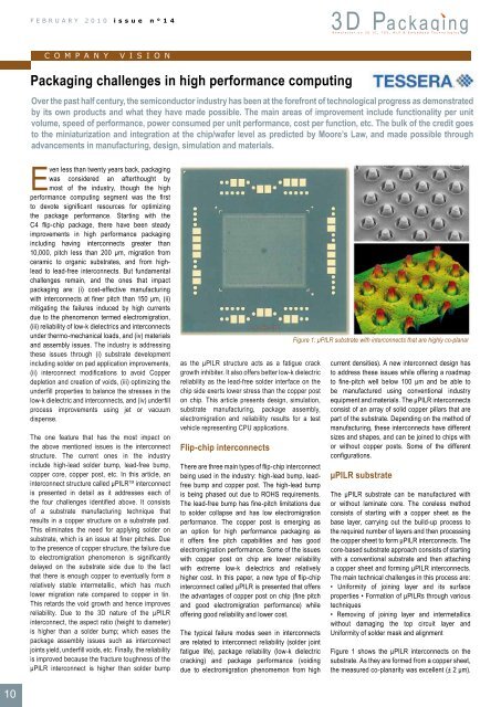
Figure 1: µPILR substrate with <str<strong>on</strong>g>in</str<strong>on</strong>g>terc<strong>on</strong>nects that are highly co-planar<br />
current densities). A new <str<strong>on</strong>g>in</str<strong>on</strong>g>terc<strong>on</strong>nect design has<br />
to address <strong>the</strong>se issues while offer<str<strong>on</strong>g>in</str<strong>on</strong>g>g a roadmap<br />
to f<str<strong>on</strong>g>in</str<strong>on</strong>g>e-pitch well below 100 µm and be able to<br />
be manufactured us<str<strong>on</strong>g>in</str<strong>on</strong>g>g c<strong>on</strong>venti<strong>on</strong>al <str<strong>on</strong>g>in</str<strong>on</strong>g>dustry<br />
equipment and materials. The µPILR <str<strong>on</strong>g>in</str<strong>on</strong>g>terc<strong>on</strong>nects<br />
c<strong>on</strong>sist of an array of solid copper pillars that are<br />
part of <strong>the</strong> substrate. Depend<str<strong>on</strong>g>in</str<strong>on</strong>g>g <strong>on</strong> <strong>the</strong> method of<br />
manufactur<str<strong>on</strong>g>in</str<strong>on</strong>g>g, <strong>the</strong>se <str<strong>on</strong>g>in</str<strong>on</strong>g>terc<strong>on</strong>nects have different<br />
sizes and shapes, and can be jo<str<strong>on</strong>g>in</str<strong>on</strong>g>ed to chips with<br />
or without copper posts. Some of <strong>the</strong> different<br />
c<strong>on</strong>figurati<strong>on</strong>s.<br />
µPILR substrate<br />
The µPILR substrate can be manufactured with<br />
or without lam<str<strong>on</strong>g>in</str<strong>on</strong>g>ate core. The coreless method<br />
c<strong>on</strong>sists of start<str<strong>on</strong>g>in</str<strong>on</strong>g>g with a copper sheet as <strong>the</strong><br />
base layer, carry<str<strong>on</strong>g>in</str<strong>on</strong>g>g out <strong>the</strong> build-up process to<br />
<strong>the</strong> required number of layers and <strong>the</strong>n process<str<strong>on</strong>g>in</str<strong>on</strong>g>g<br />
<strong>the</strong> copper sheet to form µPILR <str<strong>on</strong>g>in</str<strong>on</strong>g>terc<strong>on</strong>nects. The<br />
core-based substrate approach c<strong>on</strong>sists of start<str<strong>on</strong>g>in</str<strong>on</strong>g>g<br />
with a c<strong>on</strong>venti<strong>on</strong>al substrate and <strong>the</strong>n attach<str<strong>on</strong>g>in</str<strong>on</strong>g>g<br />
a copper sheet and form<str<strong>on</strong>g>in</str<strong>on</strong>g>g µPILR <str<strong>on</strong>g>in</str<strong>on</strong>g>terc<strong>on</strong>nects.<br />
The ma<str<strong>on</strong>g>in</str<strong>on</strong>g> technical challenges <str<strong>on</strong>g>in</str<strong>on</strong>g> this process are:<br />
• Uniformity of jo<str<strong>on</strong>g>in</str<strong>on</strong>g><str<strong>on</strong>g>in</str<strong>on</strong>g>g layer and its surface<br />
properties • Formati<strong>on</strong> of µPILRs through various<br />
techniques<br />
• Remov<str<strong>on</strong>g>in</str<strong>on</strong>g>g of jo<str<strong>on</strong>g>in</str<strong>on</strong>g><str<strong>on</strong>g>in</str<strong>on</strong>g>g layer and <str<strong>on</strong>g>in</str<strong>on</strong>g>termetallics<br />
without damag<str<strong>on</strong>g>in</str<strong>on</strong>g>g <strong>the</strong> top circuit layer and<br />
Uniformity of solder mask and alignment<br />
Figure 1 shows <strong>the</strong> µPILR <str<strong>on</strong>g>in</str<strong>on</strong>g>terc<strong>on</strong>nects <strong>on</strong> <strong>the</strong><br />
substrate. As <strong>the</strong>y are formed from a copper sheet,<br />
<strong>the</strong> measured co-planarity was excellent (± 2 µm).<br />
10


