Thin Wafer Market & Applications - I-Micronews
Thin Wafer Market & Applications - I-Micronews
Thin Wafer Market & Applications - I-Micronews
You also want an ePaper? Increase the reach of your titles
YUMPU automatically turns print PDFs into web optimized ePapers that Google loves.
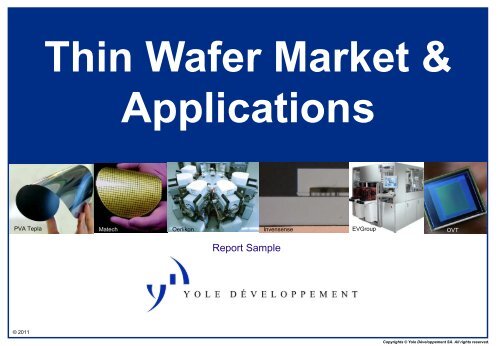
<strong>Thin</strong> <strong>Wafer</strong> <strong>Market</strong> &<br />
<strong>Applications</strong><br />
PVA Tepla Matech Oerlikon EVGroup<br />
Invensense<br />
OVT<br />
Report Sample<br />
© 2011<br />
Copyrights © Yole Développement SA. All rights reserved.
Table of Contents<br />
• Objective of the report<br />
• Table of Contents<br />
• List of companies mentioned in the report<br />
• Executive Summary<br />
• 2010-2016 <strong>Thin</strong> <strong>Wafer</strong> <strong>Market</strong> Forecasts......24<br />
– <strong>Thin</strong>ned wafers vs. TOT number of shipped wafers<br />
– <strong>Thin</strong> wafers shipment in 300 mm eq.<br />
– 2010-2016 thin wafer shipment forecast by application<br />
– 2010-2016 thin wafer shipment forecast by wafer<br />
diameter<br />
– 2010-2016 thin wafer shipment forecast by wafer<br />
thickness<br />
• <strong>Thin</strong> <strong>Wafer</strong> Players……………………………..37<br />
– 2010 main thin wafers<br />
– 2010 geographic breakdown for thin wafer processing in<br />
% of number of processed wafers<br />
– 2010 wafer size breakdown for thin wafer processing in<br />
% of number of processed wafers<br />
– <strong>Thin</strong> wafer processors<br />
• Description of applications……………..81<br />
– MEMS<br />
– CMOS Image Sensors<br />
– Power Devices<br />
– RF Devices (GaAs)<br />
– LEDs<br />
– Advanced Packaging:3D TSV/Interposers<br />
• <strong>Thin</strong> wafer technologies overview..….160<br />
– <strong>Wafer</strong> <strong>Thin</strong>ning<br />
– Dry Polishing<br />
– <strong>Thin</strong> <strong>Wafer</strong> Handling: the different solutions<br />
– <strong>Wafer</strong> Dicing<br />
• Final conclusions…………………….…214<br />
• Appendices<br />
– Yole Développement presentation<br />
© 2011• 2<br />
Copyrights © Yole Développement SA. All rights reserved.
Objective of the Report<br />
• This report provides market perspectives for thin wafer markets & applications.<br />
• It covers the following <strong>Thin</strong> <strong>Wafer</strong> applications:<br />
– MEMS<br />
– CMOS Image Sensors (incl. BSI)<br />
– Power Devices<br />
– LEDs<br />
– RF<br />
– Memory & Logic<br />
– Interposers and Advanced Packaging<br />
• For each application, market forecast in WSPY & market value ($) by wafer size<br />
and thickness, and characteristics are given (wafer size, thickness)<br />
• A ranking of the major companies worldwide processing thin wafers has been<br />
made.<br />
• In a second part, technical aspects for thin wafer manufacturing are presented:<br />
– <strong>Thin</strong>ning<br />
– Handling & temporary bonding<br />
– Dicing<br />
© 2011• 3<br />
Copyrights © Yole Développement SA. All rights reserved.
Objective of the Report<br />
• This report does NOT cover:<br />
– The report does NOT cover thinning equipment forecast.<br />
– PV application is NOT covered in this report. Current thickness is about 180-<br />
220µ and thickness could approach 100µ by 2020. But both materials and tools<br />
are VERY different from the semiconductor industry (wafers are 125x125 or<br />
156x156 mm²). <strong>Wafer</strong> thickness decrease was important a few years ago when<br />
the silicon price was at very high levels (~$400/kg, spot price, compared to<br />
$50-60/kg today). It is still interesting to decrease the wafer thickness, but with<br />
standard approaches (ingot-sawing-wafer) it is economically quite<br />
challenging; ribbon approaches (no ingot growth and sawing) provide lower<br />
quality wafers, and new approaches (ion implantation, direct wafering, etc.)<br />
are still under development.<br />
© 2011• 4<br />
Copyrights © Yole Développement SA. All rights reserved.
List of Companies Mentioned in the Report<br />
3M, Accretech, ADI, AIT, AKM, ALLVIA, ALSI, AMAT,Aptina / Micron, Avago, Brewer,<br />
Canon, Corning, Cree, Dalsa, Denka, Denso, Discera, Disco, Dongbu HiTek,<br />
DoubleCheck Semiconductors, Dynatex, Dupont, Dynatex, Elmos (SMI), Elpida, Epistar,<br />
ERS, ESI, EVG, FhG IZM, Fico, Formosa Epitaxy, Freescale, Genesis, Furukawa,<br />
Hamamatsu, HH NEC / Grace, Hitachi Chemical, Huga, Hynix, IBM , IMT, Infineon, Intel,<br />
Invensense, JCAP, Kionix, Laserod, Lextar , Lighthouse (AU Opto), LG Innotek, Lintec,<br />
Loadpoint, Lumileds, Micralyne, Micron, Misui Chemical, Nanya, Nichia, Nitta corp., Nitto<br />
Denko, Osram, Okamoto, Panasonic, PlanOptik, Powerchip, ProMOS, Renesas, Ricmar,<br />
Robert Bosch, Rorze, Samsung, Schott, Scrypt, Sekusui, Seoul Optodevice, Shinko,<br />
Silex, SMIC, Sony, Spansion, STM, Strasbaugh, Sumitomo Chemical, SUSS MicroTEC,<br />
Synova, Sysmelec, Takada, Tekcore, TEL, Texas Instruments, Tezzaron, TMAT, tMt,<br />
TOK, Toshiba , Tower, Toyoda Gosei, Tronic's, TSMC, Veeco, VTI, X fab, Xiamen Sanan<br />
Optoelectronics, Yushin.<br />
© 2011• 5<br />
Copyrights © Yole Développement SA. All rights reserved.
Why <strong>Thin</strong> <strong>Wafer</strong>s?<br />
• Consumer electronics are driving the need for smaller, higher performing, lower cost device<br />
configurations for use in applications such as memory, wireless devices...<br />
• These new options, in turn, are pushing demand for thin and even ultra-thin semiconductor<br />
wafers (below 40µm).<br />
• <strong>Thin</strong> wafer benefits are:<br />
– Reduced thickness and thus thinner packages (for cell phones, packaged dies must be < 1.2 mm<br />
thick - it is 1 mm for smart phones)<br />
– <strong>Wafer</strong> thinning is the most efficient approach used for heat dissipation for thermal management<br />
– For 3D integration, thin wafers bring higher through Si vias density as pitch and dimensions are<br />
becoming smaller<br />
• But, as wafer thickness decreases to 100µm and below, manufacturing challenges arise.<br />
Ultra-thin wafers are less stable and more vulnerable to stresses, and the die can be prone<br />
to breaking and warping—not only during grinding but also at subsequent processing steps.<br />
To address these challenges, special <strong>Wafer</strong> Support Systems have to be developed to<br />
support the wafer during backgrinding and subsequent post-thinning processes. Processes,<br />
equipment and materials for temporary bonding have ben addressed in the “<strong>Thin</strong> <strong>Wafer</strong><br />
Manufacturing” Yole report.<br />
© 2011• 6<br />
Copyrights © Yole Développement SA. All rights reserved.
From “Standard” Thickness to Ultra-thin <strong>Wafer</strong>s<br />
• The demand for ultra-thin wafers has increased in a wide range of applications such as stacked<br />
packages, portable communication devices, smart cards, cellular phones …<br />
• This, in turn, requires new handling technologies.<br />
Technology limit for handling: special equipment and<br />
processes are required (e.g. temporary bonding to a support<br />
carrier)<br />
<strong>Thin</strong> wafer<br />
drivers<br />
High interconnect<br />
density:<br />
Aggressive TSV<br />
pitch & diameters<br />
Power<br />
dissipation,<br />
higher electrical<br />
performance<br />
IC package<br />
devices:<br />
Reduced<br />
package size<br />
and thickness<br />
© 2011• 7<br />
Copyrights © Yole Développement SA. All rights reserved.
<strong>Thin</strong> <strong>Wafer</strong> <strong>Applications</strong><br />
Power Devices<br />
LEDs<br />
Interposers<br />
RF<br />
MEMS<br />
Source: Micron<br />
3D Stacking of<br />
memory, logic<br />
CMOS Image<br />
Sensors<br />
© 2011• 8<br />
Copyrights © Yole Développement SA. All rights reserved.
<strong>Thin</strong> wafers roadmap<br />
TODAY (2011) TOMORROW (2015)<br />
MEMS substrates 500-100µ<br />
MEMS capping 100-300µ<br />
ASIC MEMS 100-150µ<br />
CIS Packaging 200µ<br />
CIS BSI<br />
<strong>Wafer</strong> shipment in millions<br />
(300 mm eq.)<br />
<strong>Thin</strong>ned <strong>Wafer</strong>s vs. TOT Number of Shipped <strong>Wafer</strong>s<br />
• By 2016, we estimate the TOTAL number of thin wafers in 300 mm eq. will be 73.8 million<br />
wafers. This would represent about 55% of the total shipment for 300 mm eq. wafers<br />
• 2010-2016 CAGR for thin wafer shipment is 24%<br />
Ratio of thinned wafers vs. total number of shipped wafers<br />
(volume in millions of 300mm eq.)<br />
160<br />
140<br />
120<br />
100<br />
60%<br />
50%<br />
40%<br />
80<br />
60<br />
40<br />
20<br />
0<br />
2010 2011 2012 2013 2014 2015 2016<br />
TOT semiconductor IC wafers (12" eq.) 76 84 92 101 111 122 135<br />
TOT thin wafers (12" eq.) 20,4 25,7 31,4 38,1 48,0 60,2 73,8<br />
Ratio 27% 31% 34% 38% 43% 49% 55%<br />
30%<br />
20%<br />
10%<br />
0%<br />
© 2011• 10<br />
Copyrights © Yole Développement SA. All rights reserved.
TOP <strong>Thin</strong> <strong>Wafer</strong> Processors<br />
© 2011• 11<br />
Copyrights © Yole Développement SA. All rights reserved.
Yole activities in MEMS<br />
Media business<br />
News feed / Magazines / Webcasts<br />
<strong>Market</strong> Research<br />
Reports<br />
<strong>Market</strong> research,<br />
Technology & Strategy<br />
Consulting services<br />
www.yole.fr<br />
© 2011• 12<br />
Copyrights © Yole Développement SA. All rights reserved.
Available MEMS Reports<br />
Permanent <strong>Wafer</strong><br />
Bonding<br />
<strong>Thin</strong> <strong>Wafer</strong><br />
Handling<br />
MEMS Microphone<br />
Ferro-Electric<br />
<strong>Thin</strong> Films<br />
Trends in MEMS<br />
Manufacturing &<br />
Packaging<br />
New!<br />
New!<br />
New!<br />
New!<br />
New!<br />
Motion Sensors for<br />
Consumer & Mobile<br />
applications<br />
IMU &High<br />
Performance MEMS<br />
MEMS & Sensors<br />
for Smartphones<br />
Uncooled IR Cameras &<br />
detectors for thermography<br />
& nigh Vision<br />
CMOS Image Sensors<br />
New!<br />
MEMS Cosim+<br />
MEMS Manufacturing<br />
Cost Simulation Tool<br />
MEMS Players:<br />
Analysis of Financial<br />
Performance<br />
© 2011• 13<br />
Copyrights © Yole Développement SA. All rights reserved.


