
You also want an ePaper? Increase the reach of your titles
YUMPU automatically turns print PDFs into web optimized ePapers that Google loves.
)<br />
IMS C012<br />
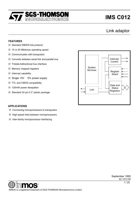
Link adaptor<br />
FEATURES<br />
H Standard INMOS link protocol<br />
H 10 or 20 Mbits/sec operating speed<br />
H Communicates with transputers<br />
H Converts between serial link and parallel bus<br />
H Tristate bidirectional bus interface<br />
H Memory mapped registers<br />
H Interrupt capability<br />
H Single +5V 5% power supply<br />
System<br />
Services<br />
Interrupt<br />
Control<br />
Register<br />
Select<br />
H TTL and CMOS compatibility<br />
H 120mW power dissipation<br />
H Standard 24 pin 0.3” plastic package<br />
Link<br />
Data and<br />
Status<br />
Registers<br />
8<br />
APPLICATIONS<br />
H Connecting microprocessors to transputers<br />
H High speed links between microprocessors<br />
H Inter-family microprocessor interfacing<br />
September 1995<br />
42 1413 05<br />
1 /25<br />
INMOS is a registered trademark of SGS-THOMSON Microelectronics Limited
Contents<br />
1 Introduction ...................................................... 3<br />
2 Pin designations .................................................. 4<br />
3 System services .................................................. 5<br />
3.1 Power ..................................................................... 5<br />
3.2 CapMinus ................................................................. 5<br />
3.3 ClockIn .................................................................... 5<br />
3.4 Reset ..................................................................... 7<br />
4 Links ............................................................. 8<br />
5 Parallel interface .................................................. 11<br />
5.1 D0–7 ...................................................................... 11<br />
5.2 notCS ..................................................................... 11<br />
5.3 RnotW .................................................................... 11<br />
5.4 RS0–1 .................................................................... 11<br />
5.5 InputInt .................................................................... 14<br />
5.6 OutputInt .................................................................. 15<br />
5.7 Data read .................................................................. 15<br />
5.8 Data write ................................................................. 15<br />
6 Electrical specifications ........................................... 16<br />
6.1 DC electrical characteristics .................................................. 16<br />
6.2 Equivalent circuits .......................................................... 17<br />
6.3 AC timing characteristics .................................................... 18<br />
6.4 Power rating ............................................................... 20<br />
7 Package details ................................................... 21<br />
7.1 Thermal specification ....................................................... 23<br />
8 Ordering .......................................................... 24<br />
2/25
1 Introduction<br />
1 Introduction<br />
The INMOS communication link is a high speed system interconnect which provides full duplex communication<br />
between transputers, according to the INMOS serial link protocol. The IMS C012 provides for full<br />
duplex transputer link communication with standard microprocessor and sub-system architectures, by<br />
converting bi-directional serial link data into parallel data streams.<br />
All products which use INMOS communication links, regardless of device type, support a standard communications<br />
frequency of 10 Mbits/sec; most products also support 20 Mbits/sec. Products of different<br />
type or performance can, therefore, be interconnected directly and future systems willbe able to communicate<br />
directly with those of today. The IMS C012 link will run at either the standard speed of 10 Mbits/sec<br />
or at the higher speed of 20 Mbits/sec. Data reception is asynchronous, allowing communication to be independent<br />
of clock phase.<br />
The IMS C012 provides an interface betweenan INMOS serial linkand a microprocessor system bus. Status<br />
and data registers for both input and output ports can be accessed across the byte-wide bi-directional<br />
interface. Two interrupt outputs are provided, one to indicate input data available and one for output buffer<br />
empty.<br />
VDD<br />
GND<br />
CapMinus<br />
ClockIn<br />
Reset<br />
LinkSpeed<br />
System<br />
Services<br />
Interrupt<br />
Control<br />
Register<br />
Select<br />
InputInt<br />
OutputInt<br />
RS0<br />
RS1<br />
RnotW<br />
notCS<br />
LinkOut<br />
LinkIn<br />
Data and<br />
Link Status<br />
Registers<br />
8 D0–7<br />
Figure 1.1<br />
IMS C012 block diagram<br />
3<br />
/25
IMS C012<br />
2 Pin designations<br />
Signal names are prefixed by not if they are active low, otherwise they are active high.<br />
Pinout details are given on page 21.<br />
Pin In/Out Function<br />
VDD, GND<br />
Power supply and return<br />
CapMinus<br />
External capacitor for internal clock power supply<br />
ClockIn in Input clock<br />
Reset in System reset<br />
LinkIn in Serial data input channel<br />
LinkOut out Serial data output channel<br />
Table 2.1<br />
Services and link<br />
Pin In/Out Function<br />
D0-7 in/out Bi-directional data bus<br />
notCS in Chip select<br />
RS0-1 in Register select<br />
RnotW in Read/write control signal<br />
InputInt out Interrupt on link receive buffer full<br />
OutputInt out Interrupt on link transmit buffer empty<br />
LinkSpeed in Select link speed as 10 or 20 Mbits/sec<br />
HoldToGND<br />
Must be connected to GND<br />
Table 2.2<br />
Parallel interface<br />
4/25
3 System services<br />
3 System services<br />
System services include all the necessary logic to start up and maintain the IMS C012.<br />
3.1 Power<br />
Power is supplied to the device via the VDD and GND pins. The supply must be decoupled close to the<br />
chip by at least one 100 nF low inductance (e.g. ceramic) capacitor between VDD and GND. Four layer<br />
boards are recommended; if two layer boards are used, extra care should be taken in decoupling.<br />
AC noise between VDD and GND must be kept below 200 mV peak to peak at all frequencies above<br />
100 KHz. AC noise between VDD and the ground reference of load capacitances must be kept below<br />
200 mV peak to peak at all frequencies above 30 MHz. Input voltages must not exceed specification with<br />
respect to VDD and GND, even during power-up and power-down ramping, otherwise latchup can occur.<br />
CMOS devices can be permanently damaged by excessive periods of latchup.<br />
3.2 CapMinus<br />
The internally derived power supply for internal clocks requires an external low leakage, low inductance<br />
1mF capacitor to be connected between VDD and CapMinus. A ceramic capacitor is preferred, with an<br />
impedance less than 3 Ohms between 100 KHz and 10 MHz. If a polarised capacitor is used the negative<br />
terminal should be connected to CapMinus. Total PCB track length should be less than 50 mm. The positive<br />
connection of the capacitor must be connected directly to VDD. Connections must not otherwise touch<br />
power supplies or other noise sources.<br />
VDD<br />
VDD pin<br />
P.C.B track<br />
Phase–locked<br />
loops<br />
Decoupling<br />
capacitor 1 mF<br />
GND<br />
CapMinus<br />
P.C.B track<br />
Figure 3.1<br />
Recommended PLL decoupling<br />
3.3 ClockIn<br />
Transputer components use a standard clock frequency, supplied by the user on the ClockIn input. The<br />
nominal frequency of this clock for all transputer components is 5 MHz, regardless of device type, transputer<br />
word length or processor cycle time. High frequency internal clocks are derived from ClockIn, simplifying<br />
system design and avoiding problems of distributing high speed clocks externally.<br />
A number of transputer devices may be connected to a common clock, or may have individual clocks providing<br />
each one meets the specified stability criteria. In a multi-clock system the relative phasing of Clock-<br />
In clocks is not important, due to the asynchronous nature of the links. Mark/space ratio is unimportant<br />
provided the specified limits of ClockIn pulse widths are met.<br />
Oscillator stability is important. ClockIn must be derived from a crystal oscillator; RC oscillators are not<br />
sufficiently stable. ClockIn must not be distributed through a long chain of buffers. Clock edges must be<br />
monotonic and remain within the specified voltage and time limits.<br />
5<br />
/25
IMS C012<br />
Symbol Parameter Min Nom Max Units Notes<br />
TDCLDCH ClockIn pulse width low 40 ns<br />
TDCHDCL ClockIn pulse width high 40 ns<br />
TDCLDCL ClockIn period 200 ns 1,3<br />
TDCerror ClockIn timing error 0.5 ns 2<br />
TDC1DC2 Difference in ClockIn for 2 linked devices 400 ppm 3<br />
TDCr ClockIn rise time 10 ns 4<br />
TDCf ClockIn fall time 8 ns 4<br />
Notes<br />
1 Measured between corresponding points on consecutive falling edges.<br />
2 Variation of individual falling edges from their nominal times.<br />
3 This value allows the use of 200ppm crystal oscillators for two devices connected together by<br />
a link.<br />
4 Clock transitions must be monotonic within the range VIH to VIL (table 6.3).<br />
Table 3.1 Input clock<br />
TDCerror<br />
TDCerror<br />
TDCerror<br />
TDCerror<br />
2.0V<br />
1.5V<br />
0.8V<br />
TDCLDCH<br />
TDCHDCL<br />
TDCLDCL<br />
90%<br />
90%<br />
10%<br />
TDCf<br />
10%<br />
TDCr<br />
Figure 3.2<br />
ClockIn timing<br />
6/25
3 System services<br />
3.4 Reset<br />
The Reset pin can go high with VDD, but must at no time exceed the maximum specified voltage for VIH.<br />
After VDD is valid ClockIn should be running for a minimum period TDCVRL before the end of Reset. All<br />
unputs, with the exception of ClockIn, SeparateIQ and LinkSpeed, must be held in their inactive state<br />
during reset.<br />
Reset initialises the IMS C012 to the following state: LinkOut is held low; the interrupt outputs InputInt<br />
and OutputInt are held low; interrupts are disabled; D0-7 are high impedance.<br />
Symbol Parameter Min Nom Max Units Notes<br />
TPVRH Power valid before Reset 10 ms<br />
TRHRL Reset pulse width high 8 ClockIn 1<br />
TDCVRL ClockIn running before Reset end 10 ms 2<br />
TRLCSL Reset low before chip select low 0 ns<br />
Notes<br />
1 Full periods of ClockIn TDCLDCL required.<br />
2 At power-on reset.<br />
Table 3.2<br />
Reset<br />
ClockIn<br />
TDCVRL<br />
VDD<br />
Reset<br />
TPVRH<br />
TRHRL<br />
TRLCSL<br />
notCS<br />
Figure 3.3<br />
Reset timing<br />
7<br />
/25
IMS C012<br />
4 Links<br />
INMOS bi-directional serial links provide synchronized communication between transputer products and<br />
the outside world. Each link comprises an input channel and output channel. A link between two devices<br />
is implemented by connecting a link interface on one device to a link interface on the other device. Every<br />
byte of data sent on a link is acknowledged on the input of the same link, thus each signal line carries both<br />
data and control information.<br />
The quiescent state of a link output is low. Each data byte is transmitted as a high start bit followed by a<br />
one bit followed by eight data bits followed by a low stop bit. The least significant bit of data is transmitted<br />
first. After transmitting a data byte the sender waits for the acknowledge, which consists of a high start bit<br />
followed by a zero bit. The acknowledge signifies both that a process was able to receive the acknowledged<br />
data byte and that the receiving link is able to receive another byte.<br />
Links are not synchronised with ClockIn and are insensitive to its phase. Thus links from independently<br />
clocked systems may communicate, providing only that the clocks arenominally identical and within specification.<br />
Links are TTL compatible and intended to be used in electrically quiet environments, between devices on<br />
a single printed circuit board or between two boards via a backplane. Direct connection may be made between<br />
devices separated by a distance of less than 300 millimetres. For longer distances a matched<br />
100 ohm transmission line should be used with series matching resistors RM. When this is done the line<br />
delay should be less than 0.4 bit time to ensure that the reflection returns before the next data bit is sent.<br />
Buffers may be used for very long transmissions. If so, their overall propagation delay should be stable<br />
within the skew tolerance of the link, although the absolute value of the delay is immaterial.<br />
The IMS C012 link supports the standard INMOS communication speed of 10 Mbits/sec. In addition it can<br />
be used at 20 Mbits/sec. Link speed can be selected by LinkSpeed; when the LinkSpeed pin is low, the<br />
link operates at the standard 10 Mbits/sec; when high it operates at 20 Mbits/sec.<br />
H H 0 1 2 3 4 5 6 7 L H L<br />
Data<br />
Ack<br />
Figure 4.1<br />
IMS C012 link data and acknowledge packets<br />
8/25
4 Links<br />
Symbol Parameter Min Nom Max Units Notes<br />
TJQr LinkOut rise time 20 ns<br />
TJQf LinkOut fall time 10 ns<br />
TJDr LinkIn rise time 20 ns<br />
TJDf LinkIn fall time 20 ns<br />
TJQJD Buffered edge delay 0 ns<br />
TJBskew Variation in TJQJD 20 Mbits/s 3 ns 1<br />
10 Mbits/s 10 ns 1<br />
CLIZ LinkIn capacitance @ f=1MHz 7 pF<br />
CLL LinkOut load capacitance 50 pF<br />
RM Series resistor for 100Wtransmission line 56 ohms<br />
Notes<br />
1 This is the variation in the total delay through buffers, transmission lines, differential receivers<br />
etc., caused by such things as short term variation in supply voltages and differences in delays<br />
for rising and falling edges.<br />
Table 4.1<br />
Link<br />
LinkOut<br />
90%<br />
10%<br />
TJQr<br />
TJQf<br />
LinkIn<br />
90%<br />
10%<br />
TJDr<br />
TJDf<br />
Figure 4.2<br />
IMS C012 link timing<br />
LinkOut<br />
1.5 V<br />
Latest TJQJD<br />
Earliest TJQJD<br />
LinkIn<br />
1.5 V<br />
TJBskew<br />
Figure 4.3<br />
IMS C012 buffered link timing<br />
9<br />
/25
IMS C012<br />
Transputer device A<br />
LinkOut<br />
LinkIn<br />
LinkIn<br />
LinkOut<br />
Transputer device B<br />
Figure 4.4<br />
Links directly connected<br />
Transputer device A<br />
LinkOut<br />
RM<br />
Zo=100 ohms<br />
LinkIn<br />
LinkIn<br />
Zo=100 ohms<br />
RM<br />
LinkOut<br />
Transputer device B<br />
Figure 4.5<br />
Links connected by transmission line<br />
Transputer device A<br />
LinkOut<br />
LinkIn<br />
buffers<br />
LinkIn<br />
LinkOut<br />
Transputer device B<br />
Figure 4.6<br />
Links connected by buffers<br />
10 /25
5 Parallel interface<br />
5 Parallel interface<br />
The IMS C012 provides an interface between a link and a microprocessor style bus. Operation of the link<br />
adaptor is controlled through the parallel interface bus lines D0-7 by reading and writing various registers<br />
in the link adaptor. Registers are selected by RS0-1 and RnotW, and the chip enabled with notCS.<br />
For convenience of description, the device connected to the parallel side of the link adaptor is presumed<br />
to be a microprocessor, although this will not always be the case.<br />
5.1 D0–7<br />
Data is communicated between a microprocessor bus and the link adaptor via the bidirectional bus lines<br />
D0-7. The bus is high impedance unless the link adaptor chip is selected and the RnotW line is high. The<br />
bus is used by the microprocessor to access status and data registers.<br />
5.2 notCS<br />
The link adaptor chip is selected when notCS is low. Register selectors RS0-1 and RnotW must be valid<br />
before notCS goes low; D0-7 must also be valid if writing to the chip (RnotW low). Data is read by the link<br />
adaptor on the rising edge of notCS.<br />
5.3 RnotW<br />
RnotW, in conjunction with notCS, selects the link adaptor registers for read or write mode. When RnotW<br />
is high, the contents of an addressed register appear on the data bus D0-7; when RnotW is low the data<br />
on D0-7 is written into the addressed register. The state of RnotW is latched into the link adaptor by notCS<br />
going low; it may be changed before notCS returns high, within the timing restrictions given.<br />
5.4 RS0–1<br />
One of four registers is selected by RS0-1. A register is addressed by setting up RS0-1 and then taking<br />
notCS low; the state of RnotW when notCS goes low determines whether the register will be read or written.<br />
The state of RS0-1 is latched into the link adaptor by notCS going low; it may be changed before<br />
notCS returns high, within the timing restrictions given. The register set comprises a read-only data input<br />
register, a write-only data output register and a read/write status register for each.<br />
RS1 RS0 RnotW Register<br />
0 0 1 Read data<br />
0 0 0 Invalid<br />
0 1 1 Invalid<br />
0 1 0 Write data<br />
1 0 1 Read input status<br />
1 0 0 Write input status<br />
1 1 1 Read output status<br />
1 1 0 Write output status<br />
Table 5.1<br />
IMS C012 register selection<br />
5.4.1 Input Data Register<br />
This register holds the last data packet received from the serial link. It never contains acknowledge packets.<br />
It contains valid data only whilst the data present flag is set in the input status register. It cannot be<br />
assumed to contain valid data after it has been read; a double read may or may not return valid data on<br />
11<br />
/25
IMS C012<br />
the second read. If data present is valid on a subsequent read it indicates new data is in the buffer. Writing<br />
to this register will have no effect.<br />
Symbol Parameter Min Nom Max Units Note<br />
TRSVCSL Register select setup 5 ns<br />
TCSLRSX Register select hold 8 ns<br />
TRWVCSL Read/write strobe setup 5 ns<br />
TCSLRWX Read/write strobe hold 8 ns<br />
TCSLCSH Chip select active 60 ns<br />
TCSHCSL Delay before re-assertion of chip select 50 ns<br />
Table 5.2<br />
IMS C012 parallel interface control<br />
Symbol Parameter Min Nom Max Units Note<br />
TLdVIIH Start of link data to InputInt high 14 bits 1<br />
TCSLIIL Chip select to InputInt low 35 ns<br />
TCSLDrX Chip select to bus active 5 ns<br />
TCSLDrV Chip select to data valid 50 ns<br />
TCSHDrZ Chip select high to bus tristate 38 ns<br />
TCSHDrX Data hold after chip select high 5 ns<br />
TCSHLaV Chip de-select to start of Ack 0.8 2.5 bits 1,2<br />
Notes<br />
1 Unit of measurement is one link data bit time; at 10 Mbits/s data link speed, one bit time is nominally<br />
100 ns.<br />
2 Maximum time assumes there is no acknowledge packet already on the link. Maximum time with<br />
acknowledge on the link is extended by 11 bits.<br />
Table 5.3 IMS C012 parallel interface read<br />
LinkIn<br />
InputInt<br />
Data<br />
TLdVIIH<br />
Data<br />
TCSLIIL<br />
RS0–1<br />
TRSVCSL<br />
TCSLRSX<br />
RnotW<br />
TRWVCSL<br />
TCSLRSX<br />
TCSLCSH TCSHCSL<br />
notCS<br />
D0–7<br />
LinkOut<br />
TCSLDrV<br />
TCSLDrX<br />
TCSHDrZ<br />
TCSHDrX<br />
TCSHLaV<br />
Ack<br />
Figure 5.1<br />
IMS C012 read parallel data from link adaptor<br />
12 /25
5 Parallel interface<br />
Symbol Parameter Min Nom Max Units Note<br />
TCSHDwV Data setup 10 ns<br />
TCSHDwX Data hold 10 ns<br />
TCSLOIL Chip select to OutputInt low 35 ns<br />
TCSHLdV Chip select high to start of link data 0.8 2.5 bits 1,2<br />
TLaVOIH Start of link Ack to OutputInt high 3.3 bits 1,3<br />
TLdVOIH Start of link data to OutputInt high 13 bits 1,3<br />
Notes<br />
1 Unit of measurement is one link data bit time; at 10 Mbits/s data link speed, one bit time is nominally<br />
100 ns.<br />
2 Maximum time assumes there is no acknowledge packet already on the link. Maximum time with<br />
acknowledge on the link is extended by 2 bits.<br />
3 Both data transmission and the returned acknowledge must be completed before OutputInt can<br />
go high.<br />
Table 5.4<br />
IMS C012 parallel interface write<br />
RS0–1<br />
TRSVCSL<br />
TCSLRSX<br />
RnotW<br />
TRWVCSL<br />
TCSLRWX<br />
TCSLCSH TCSHCSL<br />
notCS<br />
TCSHDwV<br />
TCSHDwX<br />
D0–7<br />
OutputInt<br />
LinkOut<br />
LinkIn<br />
TCSLOIL<br />
TCSHLdV<br />
TLdVOIH<br />
Data<br />
TLaVOIH<br />
Ack<br />
Figure 5.2<br />
IMS C012 write parallel data to link adaptor<br />
13<br />
/25
IMS C012<br />
5.4.2 Input Status Register<br />
This register contains the data present flag and the interrupt enable control bit for InputInt. The data present<br />
flag is set to indicate that data in the data input buffer is valid. It is reset low only when the data input<br />
buffer is read, or by Reset. When writing to this register, the data present bit must be written as zero.<br />
The interrupt enable bit can be set and reset by writing to the status register with this bit high or low respectively.When<br />
the interrupt enable and data present flags are both high, theInputInt output will be high (section<br />
5.5). Resetting interrupt enable will take InputInt low; setting it again before reading the data input<br />
register will set InputInt high again. The interrupt enable bit can be read to determine its status.<br />
When writing to this register, bits 2-7 must be written as zero; this ensures that they will be zero when the<br />
register is read. Failure to write zeroes to these bits may result in undefined data being returned by these<br />
bits during a status register read.<br />
7 6 5 4 3 2 1 0<br />
Interrupt<br />
Enable<br />
Data<br />
Present<br />
&<br />
InputInt<br />
Figure 5.3<br />
IMS C012 input status register<br />
5.4.3 Output Data Register<br />
Data written to this link adaptor register is transmitted out of the serial link as a data packet. Data should<br />
only be written to this register when the output ready bit in the output status register is high, otherwise data<br />
already being transmitted may be corrupted. Reading this register will result in undefined data being read.<br />
5.4.4 Output Status Register<br />
This register contains the output ready flag and the interrupt enable control bit for OutputInt. The output<br />
ready flag is set to indicate that the data output buffer is empty. It is reset low only when data is written to<br />
the data output buffer; it is set high by Reset. When writing to this register, the output ready bit must be<br />
written as zero.<br />
The interrupt enable bit can be set and reset by writing to the status register with this bit high or low respectively.<br />
When the interrupt enable and output ready flags are both high, the OutputInt output will be high<br />
(section 5.6). Resetting interrupt enable will take OutputInt low; setting it again whilst the data output register<br />
is empty will set OutputInt high again. The interrupt enable bit can be read to determine its status.<br />
When writing to this register, bits 2-7 must be written as zero; this ensures that they will be zero when the<br />
register is read. Failure to write zeroes to these bits may result in undefined data being returned by these<br />
bits during a status register read.<br />
5.5 InputInt<br />
The InputInt output is set high to indicate that a data packet has been received from the serial link. It is<br />
inhibited from going high when the interrupt enable bit in the input status register is low (section 5.4.2).<br />
InputInt is reset low when data is read from the input data register (section 5.4.1) and by Reset (page 7).<br />
14 /25
5 Parallel interface<br />
7 6 5 4 3 2 1 0<br />
Interrupt<br />
Enable<br />
Output<br />
Ready<br />
&<br />
OutputInt<br />
Figure 5.4<br />
IMS C012 output status register<br />
5.6 OutputInt<br />
The OutputInt output is set high to indicate that the link is free to receive data from the microprocessor<br />
for transmission as a data packet out of the serial link. It is inhibited from going high when the interrupt<br />
enable bit in the output status register is low (section 5.4.4). OutputInt is reset low when data is written<br />
to the data output register; it is set low by Reset (page 7).<br />
5.7 Data read<br />
A data packet received on the input link sets the data present flag in the input status register. If the interrupt<br />
enable bit in the status register is set, the InputInt output pin will be set high. Themicroprocessor willeither<br />
respond to the interrupt (if the interrupt enable bit is set) or will periodically read the input status register<br />
until the data present bit is high.<br />
When data is availablefrom the link, the microprocessor reads the data packet fromthe data input register.<br />
This will reset the data present flag and cause the link adaptor to transmit an acknowledge packet out of<br />
the serial link output. InputInt is automatically reset by reading the data input register; it is not necessary<br />
to read or write the input status register.<br />
5.8 Data write<br />
When the data output buffer is empty the output ready flag in the output status register is set high. If the<br />
interrupt enable bit in the status register is set, the OutputInt output pin will also be set high. The microprocessor<br />
will either respond to the interrupt (if the interrupt enable bit is set) or will periodically read the output<br />
status register until the output ready bit is high.<br />
When the output ready flag is high, the microprocessor can write data to the data output buffer. This will<br />
result in the link adaptor resetting the output ready flag and commencing transmission of the data packet<br />
out of the serial link. The output ready status bit will remain low until the data byte transmission has been<br />
completed and an acknowledge packet is received by the input link. This will set the output ready flag high;<br />
if the interrupt enable bit is set, OutputInt will also be set high.<br />
15<br />
/25
IMS C012<br />
6 Electrical specifications<br />
6.1 DC electrical characteristics<br />
SYMBOL PARAMETER MIN MAX UNITS NOTES<br />
VDD DC supply voltage 0 7.0 V 1,2,3<br />
VI, VO Voltage on input and output pins –0.5 VDD+0.5 V 1,2,3<br />
II Input current 25 mA 4<br />
tOSC Output short circuit time (one pin) 1 s 2<br />
TS Storage temperature –65 150 o C 2<br />
TA Ambient temperature under bias –55 125 o C 2<br />
PDmax Maximum allowable dissipation 600 mW<br />
Notes<br />
1 All voltages are with respect to GND.<br />
2 This is a stress rating only and functional operation of the device at these or any other conditions<br />
beyond those indicated in the operating sections of this specification is not implied. Stresses<br />
greater than those listed may cause permanent damage to the device. Exposure to absolute<br />
maximum rating conditions for extended periods may affect reliability.<br />
3 This device contains circuitry to protect the inputs againstdamage caused by high static voltages<br />
or electrical fields. However, it is advised that normal precautions be taken to avoid application<br />
of any voltage higher than the absolute maximum rated voltages to this high impedance circuit.<br />
Unused inputs should be tied to an appropriate logic level such as VDD or GND.<br />
4 The input current applies to any input or output pin and applies when the voltage on the pin is<br />
between GND and VDD.<br />
Table 6.1 Absolute maximum ratings<br />
SYMBOL PARAMETER MIN MAX UNITS NOTES<br />
VDD DC supply voltage 4.75 5.25 V 1<br />
VI, VO Input or output voltage 0 VDD V 1,2<br />
CL Load capacitance on any pin 60 pF<br />
TA Operating temperature range 0 70 o C 3<br />
Notes<br />
1 All voltages are with respect to GND.<br />
2 Excursions beyond the supplies are permitted but not recommended; see DC characteristics.<br />
3 Air flow rate 400 linear ft/min transverse air flow.<br />
Table 6.2 Operating conditions<br />
16 /25
6 Electrical specifications<br />
Symbol Parameter Min Max Units Notes<br />
VIH High level input voltage 2.0 VDD+0.5 V 1,2<br />
VIL Low level input voltage –0.5 0.8 V 1,2<br />
II Input current @ GND
IMS C012<br />
Inputs<br />
VDD–1<br />
0V<br />
VIH<br />
Inputs<br />
VDD–1<br />
0V<br />
VIL<br />
tpHL<br />
Outputs<br />
VDD<br />
0V<br />
tpLH<br />
1.5V<br />
Outputs<br />
VDD<br />
0V<br />
1.5V<br />
Figure 6.2<br />
AC measurements timing waveforms<br />
6.3 AC timing characteristics<br />
Symbol Parameter Min Max Units Notes<br />
TDr Input rising edges 2 20 ns 1, 2<br />
TDf Input falling edges 2 20 ns 1, 2<br />
TQr Output rising edges 25 ns 1<br />
TQf Output falling edges 15 ns 1<br />
TCSLaHZ Chip select high to tristate 25 ns<br />
TCSLaLZ Chip select low to tristate 25 ns<br />
Notes<br />
1 Non-link pins; see section on links.<br />
2 All inputs except ClockIn; see section on ClockIn.<br />
Table 6.4 Input and output edges<br />
18 /25
6 Electrical specifications<br />
90%<br />
90%<br />
10%<br />
10%<br />
TDf<br />
TDr<br />
90%<br />
90%<br />
10%<br />
10%<br />
TQf<br />
TQr<br />
Figure 6.3<br />
IMS C012 input and output edge timing<br />
1.5 V<br />
1.5 V<br />
90%<br />
TCSLaHZ<br />
10%<br />
TCSLaLZ<br />
Figure 6.4<br />
IMS C012 tristate timing relative to notCS<br />
30<br />
30<br />
Rise time<br />
Time<br />
ns<br />
20<br />
10<br />
Rise time<br />
Fall time<br />
20<br />
Time<br />
ns<br />
10<br />
Fall time<br />
40 60 80 100<br />
Load capacitance pF<br />
Link<br />
40 60 80 100<br />
Load capacitance pF<br />
Non Links<br />
Figure 6.5<br />
Typical rise/fall times<br />
19<br />
/25
IMS C012<br />
6.4 Power rating<br />
Internal power dissipation (P INT ) of transputer and peripheral chips depends on VDD, as shown in<br />
figure 6.6. P INT is substantially independent of temperature.<br />
200<br />
Power<br />
P INT<br />
(mW)<br />
150<br />
100<br />
50<br />
4.4 4.6 4.8 5.0 5.2 5.4 5.6<br />
VDD (Volts)<br />
Figure 6.6<br />
IMS C012 internal power dissipation vs VDD<br />
Total power dissipation (P D ) of the chip is<br />
P D = P INT + P IO<br />
where P IO is the power dissipation in the input and output pins; this is application dependent.<br />
Internal working temperature T J of the chip is<br />
T J = T A + q JA * P D<br />
where T A is the external ambient temperature in o C and q JA is the junction-to-ambient thermal resistance<br />
in o C/W.<br />
Further information about device thermal characteristics can be found in section 7.1.<br />
20 /25
7 Package details<br />
7 Package details<br />
Figure 7.1<br />
IMS C012 24-pin dual-in-line (DIL) package pinout<br />
21<br />
/25
IMS C012<br />
Figure 7.2<br />
IMS C012 24-pin dual-in-line (DIL) package dimensions<br />
22 /25
7 Package details<br />
7.1 Thermal specification<br />
The IMS C012 is tested to a maximum silicon temperature of 100_C. For operation within thegiven specifications,<br />
the case temperature should not exceed 85_C.<br />
For temperatures above 85_C the operation of the device cannot be guaranteed and reliability may be<br />
impaired.<br />
For further information on reliability refer to the SGS–THOMSON Microelectronics Quality and Reliability<br />
Program.<br />
23<br />
/25
IMS C012<br />
8 Ordering<br />
This section indicates the designation of package selections for the IMS C012. Speed of ClockIn is 5 MHz<br />
for all parts.<br />
For availability contact your local SGS–THOMSON sales office or authorized distributor.<br />
SGS–THOMSON designation<br />
IMS C012-P20S<br />
Package<br />
24 pin plastic dual-in-line<br />
Table 8.1<br />
IMS C012 ordering details<br />
24 /25
Information furnished is believed to be accurate and reliable. However, SGS-THOMSON Microelectronics assumes no<br />
responsibility for the consequences of use of such information nor for any infringement of patents or other rights of third<br />
parties which may result from its use. No license is granted by implication or otherwise under any patent or patent rights of<br />
SGS-THOMSON Microelectronics. Specifications mentioned in this publication are subject to change without notice. This<br />
publication supersedes and replaces all information previously supplied. SGS-THOMSON Microelectronics products are not<br />
authorized for use as critical components in life support devices or systems without express written approval of SGS-THOM-<br />
SON Microelectronics.<br />
E 1995 SGS-THOMSON Microelectronics - All Rights Reserved<br />
, , IMS, occam and DS-Link are trademarks of SGS-THOMSON Microelectronics Limited.<br />
is a registered trademark of the SGS-THOMSON Microelectronics Group.<br />
SGS-THOMSON Microelectronics GROUP OF COMPANIES<br />
Australia - Brazil - France - Germany - Hong Kong - Italy - Japan - Korea - Malaysia - Malta - Morocco -<br />
The Netherlands - Singapore - Spain - Sweden - Switzerland - Taiwan - Thailand - United Kingdom - U.S.A.<br />
25 /25