Development and evolution of MOEMS technology in variable ...
Development and evolution of MOEMS technology in variable ...
Development and evolution of MOEMS technology in variable ...

Create successful ePaper yourself
Turn your PDF publications into a flip-book with our unique Google optimized e-Paper software.
Lee <strong>and</strong> Yeh: <strong>Development</strong> <strong>and</strong> <strong>evolution</strong> <strong>of</strong> <strong>MOEMS</strong> <strong>technology</strong>…<br />
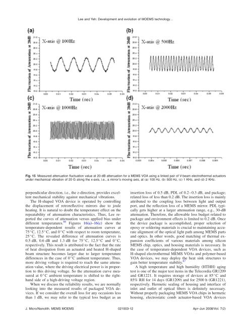
Fig. 15 Measured attenuation fluctuation value at 20-dB attenuation for a MEMS VOA us<strong>in</strong>g a l<strong>in</strong>ked pair <strong>of</strong> V-beam electrothermal actuators<br />
under mechanical vibration <strong>of</strong> 20 G along the x-axis, i.e., a mirror’s mov<strong>in</strong>g axis, at a 100 Hz, b 500 Hz, c 1 KHz, <strong>and</strong> d 2 KHz.<br />
perpendicular direction, i.e., the z-direction, provides excellent<br />
mechanical stability aga<strong>in</strong>st mechanical vibrations.<br />
The H-shaped VOA device is operated by controll<strong>in</strong>g<br />
the displacement <strong>of</strong> retroreflective mirrors due to joule<br />
heat<strong>in</strong>g. It is natural to doubt the temperature effect on the<br />
repeatability <strong>of</strong> attenuation characteristics. Thus, Lee reported<br />
the curves <strong>of</strong> attenuation versus applied bias under<br />
different temperatures. 66 Figures 16a–16c show the<br />
temperature-dependent results <strong>of</strong> attenuation curves at<br />
75°C, 12.5°C, <strong>and</strong> 0°C with respect to room temperature,<br />
25°C. The revealed difference <strong>of</strong> attenuation curves is<br />
0.5 dB, 0.6 dB <strong>and</strong> 1.3 dB for 75°C, 12.5°C <strong>and</strong> 0°C,<br />
respectively. This result is attributed to the fact that the rate<br />
<strong>of</strong> heat dissipation from an actuated <strong>and</strong> heated H-shaped<br />
beam structure becomes larger due to larger temperature<br />
differences <strong>in</strong> the case <strong>of</strong> 0°C ambient temperature. Thus,<br />
more driv<strong>in</strong>g voltage is required to reach the same attenuation<br />
value, where the driv<strong>in</strong>g electrical power is <strong>in</strong> proportion<br />
to this driv<strong>in</strong>g voltage. So the attenuation curve measured<br />
at 0°C ambient temperature is shifted to the righth<strong>and</strong><br />
side <strong>of</strong> a high-driv<strong>in</strong>g voltage region.<br />
When we discuss the reliability results, we are normally<br />
look<strong>in</strong>g <strong>in</strong>to the measured results <strong>of</strong> packaged VOA devices.<br />
If we consider the overall loss for any occasions less<br />
than 1 dB, we may refer to the typical loss budget as an<br />
<strong>in</strong>sertion loss <strong>of</strong> 0.5 dB, PDL <strong>of</strong> 0.2–0.3 dB, <strong>and</strong> package;<br />
related loss <strong>of</strong> less than 0.2 dB. The <strong>in</strong>sertion loss is ma<strong>in</strong>ly<br />
attributed to the coupl<strong>in</strong>g loss between light <strong>and</strong> output<br />
port, <strong>and</strong> the reflection loss <strong>of</strong> a MEMS mirror. PDL typically<br />
gets higher at a larger attenuation range, e.g., 30-dB<br />
attenuation. Therefore, the allowable loss budget related to<br />
package <strong>and</strong> environment effects is limited to 0.2 dB. Once<br />
the device package is accomplished, proper selection <strong>of</strong><br />
epoxy or solder<strong>in</strong>g materials is crucial to ma<strong>in</strong>ta<strong>in</strong><strong>in</strong>g accurate<br />
alignment <strong>of</strong> the optical light path among MEMS parts<br />
<strong>and</strong> optics. In other words, good match<strong>in</strong>g <strong>of</strong> thermal expansion<br />
coefficients <strong>of</strong> various materials among silicon<br />
MEMS chip, optics, <strong>and</strong> hous<strong>in</strong>g materials is necessary. In<br />
the case <strong>of</strong> temperature-dependent VOA devices, such as<br />
H-shaped electrothermal MEMS VOAs <strong>and</strong> polymer-based<br />
VOA devices, we may deploy the heat s<strong>in</strong>k structures to<br />
ga<strong>in</strong> better temperature stability. 67<br />
A high temperature <strong>and</strong> high humidity HTHH ag<strong>in</strong>g<br />
test is one <strong>of</strong> the major test items <strong>in</strong> the Telecordia GR1209<br />
<strong>and</strong> GR1221. It requires storage <strong>of</strong> devices at 85°C <strong>and</strong><br />
85% RH for 14 days GR1209 <strong>and</strong> for 2500 h GR1221,<br />
respectively. Hermetic seal<strong>in</strong>g <strong>of</strong> hous<strong>in</strong>g <strong>and</strong> <strong>in</strong>terface <strong>of</strong><br />
<strong>in</strong>let <strong>and</strong> outlet <strong>of</strong> optical fibers is def<strong>in</strong>itely necessary.<br />
Without properly packag<strong>in</strong>g MEMS VOA chips <strong>in</strong> hermetic<br />
hous<strong>in</strong>g, electrostatic comb actuator-based VOA devices<br />
J. Micro/Nanolith. MEMS <strong>MOEMS</strong> 021003-12<br />
Apr–Jun 2008/Vol. 72