Development and evolution of MOEMS technology in variable ...
Development and evolution of MOEMS technology in variable ...
Development and evolution of MOEMS technology in variable ...

Create successful ePaper yourself
Turn your PDF publications into a flip-book with our unique Google optimized e-Paper software.
Lee <strong>and</strong> Yeh: <strong>Development</strong> <strong>and</strong> <strong>evolution</strong> <strong>of</strong> <strong>MOEMS</strong> <strong>technology</strong>…<br />
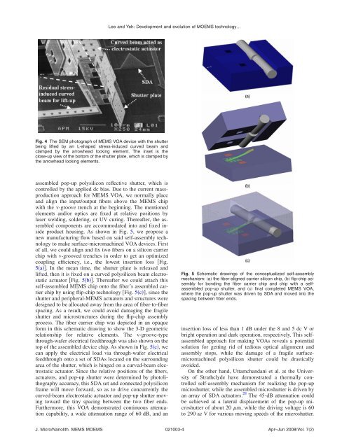
Fig. 4 The SEM photograph <strong>of</strong> MEMS VOA device with the shutter<br />
be<strong>in</strong>g lifted by an L-shaped stress-<strong>in</strong>duced curved beam <strong>and</strong><br />
clamped by the arrowhead lock<strong>in</strong>g element. The <strong>in</strong>set is the<br />
close-up view <strong>of</strong> the bottom <strong>of</strong> the shutter plate, which is clamped by<br />
the arrowhead lock<strong>in</strong>g elements.<br />
assembled pop-up polysilicon reflective shutter, which is<br />
controlled by the applied dc bias. Due to the current massproduction<br />
approach for MEMS VOA, we normally place<br />
<strong>and</strong> align the <strong>in</strong>put/output fibers above the MEMS chip<br />
with the v-groove trench at the beg<strong>in</strong>n<strong>in</strong>g. The mentioned<br />
elements <strong>and</strong>/or optics are fixed at relative positions by<br />
laser weld<strong>in</strong>g, solder<strong>in</strong>g, or UV cur<strong>in</strong>g. Thereafter, the assembled<br />
components are accommodated <strong>in</strong>to <strong>and</strong> fixed <strong>in</strong>side<br />
product hous<strong>in</strong>g. As shown <strong>in</strong> Fig. 5, we propose a<br />
new manufactur<strong>in</strong>g flow based on said self-assembly <strong>technology</strong><br />
to make surface-micromach<strong>in</strong>ed VOA devices. First<br />
<strong>of</strong> all, we could align <strong>and</strong> fix two fibers on a silicon carrier<br />
chip with v-grooved trenches <strong>in</strong> order to get an optimized<br />
coupl<strong>in</strong>g efficiency, i.e., the lowest <strong>in</strong>sertion loss Fig.<br />
5a. In the mean time, the shutter plate is released <strong>and</strong><br />
lifted, then it is fixed on a curved polysilicon beam electrostatic<br />
actuator Fig. 5b. Thereafter we could attach this<br />
self-assembled MEMS chip onto the fiber’s assembled carrier<br />
chip by us<strong>in</strong>g flip-chip <strong>technology</strong> Fig. 5c, s<strong>in</strong>ce the<br />
shutter <strong>and</strong> peripheral-MEMS actuators <strong>and</strong> structures were<br />
designed to be allocated away from the area <strong>of</strong> fiber-to-fiber<br />
spac<strong>in</strong>g. As a result, we could avoid damag<strong>in</strong>g the fragile<br />
shutter <strong>and</strong> microstructures dur<strong>in</strong>g the flip-chip assembly<br />
process. The fiber carrier chip was depicted <strong>in</strong> an opaque<br />
form <strong>in</strong> this schematic draw<strong>in</strong>g to show the 3-D geometric<br />
relationship for relative elements. The v-groove-type<br />
through-wafer electrical feedthrough was also shown on the<br />
top <strong>of</strong> the assembled device chip. As shown <strong>in</strong> Fig. 5c, we<br />
can apply the electrical load via through-wafer electrical<br />
feedthrough onto a set <strong>of</strong> SDAs located on the surround<strong>in</strong>g<br />
area <strong>of</strong> the shutter, which is h<strong>in</strong>ged on a curved-beam electrostatic<br />
actuator. S<strong>in</strong>ce the relative positions <strong>of</strong> the fibers,<br />
actuators, <strong>and</strong> pop-up shutter were determ<strong>in</strong>ed by photolithography<br />
accuracy, this SDA set <strong>and</strong> connected polysilicon<br />
frame will move forward, so as to drive concurrently the<br />
curved-beam electrostatic actuator <strong>and</strong> pop-up shutter mov<strong>in</strong>g<br />
toward the t<strong>in</strong>y spac<strong>in</strong>g between the two fiber ends.<br />
Furthermore, this VOA demonstrated cont<strong>in</strong>uous attenuation<br />
capability, a wide attenuation range <strong>of</strong> 60 dB, <strong>and</strong> an<br />
Fig. 5 Schematic draw<strong>in</strong>gs <strong>of</strong> the conceptualized self-assembly<br />
mechanism: a the fiber-aligned carrier silicon chip, b flip-chip assembly<br />
for bond<strong>in</strong>g the fiber carrier chip <strong>and</strong> chip with a selfassembled<br />
pop-up shutter, <strong>and</strong> c f<strong>in</strong>al completed MEMS VOA,<br />
where the pop-up shutter was driven by SDA <strong>and</strong> moved <strong>in</strong>to the<br />
spac<strong>in</strong>g between fiber ends.<br />
<strong>in</strong>sertion loss <strong>of</strong> less than 1 dB under the 8 <strong>and</strong> 5 dc V or<br />
bright operation <strong>and</strong> dark operation, respectively. This selfassembled<br />
approach for mak<strong>in</strong>g VOAs reveals a potential<br />
solution for gett<strong>in</strong>g rid <strong>of</strong> tedious optical alignment <strong>and</strong><br />
assembly stops, while the damage <strong>of</strong> a fragile surfacemicromach<strong>in</strong>ed<br />
polysilicon shutter could be drastically<br />
avoided.<br />
On the other h<strong>and</strong>, Uttamch<strong>and</strong>ani et al. at the University<br />
<strong>of</strong> Strathclyde have demonstrated a thermally controlled<br />
self-assembly mechanism for realiz<strong>in</strong>g the pop-up<br />
microshutter, while the assembled microshutter is driven by<br />
an array <strong>of</strong> SDA actuators. 28 The 45-dB attenuation could<br />
be achieved at a lateral displacement <strong>of</strong> the pop-up microshutter<br />
<strong>of</strong> about 20 m, while the driv<strong>in</strong>g voltage is 60<br />
to 290 ac V for various mov<strong>in</strong>g speeds <strong>of</strong> the microshutter.<br />
J. Micro/Nanolith. MEMS <strong>MOEMS</strong> 021003-4<br />
Apr–Jun 2008/Vol. 72