Download
Download
Download

You also want an ePaper? Increase the reach of your titles
YUMPU automatically turns print PDFs into web optimized ePapers that Google loves.
35 4<br />
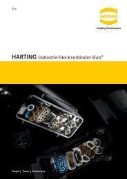
HARTING<br />
TCA Connectors<br />
People | Power | Partnership
HARTING worldwide<br />
Transforming customer wishes<br />
into concrete solutions<br />
2<br />
The HARTING Technology Group is skilled in the fields of electrical, electronic and optical connection,<br />
transmission and networking, as well as in manufacturing, mechatronics and software creation.<br />
The Group uses these skills to develop customized solutions and products such as connectors for energy and<br />
data transmission applications including, for example, mechanical engineering, rail technology, wind energy<br />
plants, factory automation and the telecommunications sector. In addition, HARTING also produces electromagnetic<br />
components for the automobile industry and offers solutions in the field of Enclosures and Shop<br />
Systems.<br />
The HARTING Group currently comprises 32 subsidiary companies and worldwide distributors employing a total<br />
of approx. 3,000 staff.
HARTING Subsidiary company<br />
HARTING Representatives<br />
ALWAYS at hand, wherever our customers may be.<br />
Increasing industrialization is creating growing markets<br />
characterized by widely diverging demands and requirements. The<br />
search for perfection, increasingly efficient processes and reliable<br />
technologies is a common factor in all sectors across the globe.<br />
HARTING is providing these technologies – in Europe, America and<br />
Asia. The HARTING professionals at our international subsidiaries<br />
engage in close, partnership based interaction with our customers,<br />
right from the very early product development phases, in order to<br />
realize customer demands and requirements in the best possible<br />
manner.<br />
Our people on location form the interface to the centrally<br />
coordinated development and production departments. In this<br />
way, our customers can rely on consistently high, superior product<br />
quality – worldwide.<br />
we aspire to top performance.<br />
Connectors ensure functionality. As core elements of electrical<br />
and optical wiring, connection and infrastructure technologies,<br />
they are essential in enabling the modular construction of<br />
devices, machines and systems across a very wide range of<br />
industrial applications. Their reliability is a crucial factor<br />
guaranteeing smooth functioning in the manufacturing area,<br />
in telecommunications, applications in medical technology<br />
– in fact, connectors are at work in virtually every conceivable<br />
application area. Thanks to the consistent further development of<br />
our technologies, customers enjoy investment security and benefit<br />
from durable, long term functionality.<br />
our claim: pusHing performance.<br />
HARTING provides more than optimally attuned components. In<br />
order to serve our customers with the best possible solutions,<br />
HARTING is able to contribute a great deal more and play a closely<br />
integrative role in the value creation process.<br />
From ready assembled cables through to control racks or ready-togo<br />
control desks: Our aim is to generate the maximum benefits for<br />
our customers – without compromise!<br />
QuaLity creates reliability – and warrants trust.<br />
The HARTING brand stands for superior quality and reliability<br />
– worldwide. The standards we set are the result of consistent,<br />
stringent quality management that is subject to regular<br />
certifications and audits.<br />
EN ISO 9001, the EU Eco-Audit and ISO 14001:2004 are key<br />
elements here. We take a proactive stance to new requirements,<br />
which is why HARTING ranks among the first companies<br />
worldwide to have obtained the new IRIS quality certificate<br />
for rail vehicles.<br />
3
The HARTING Technology Group<br />
Harting tecHnoLogy creates added value for<br />
customers.<br />
Technologies by HARTING are at work worldwide. HARTING’s<br />
presence stands for smoothly functioning systems, powered<br />
by intelligent connectors, smart infrastructure solutions and<br />
mature network systems. In the course of many years of close,<br />
trust-based cooperation with its customers, the HARTING<br />
Technology Group has advanced to one of the worldwide leading<br />
specialists for connector technology. Extending beyond the<br />
basic functionalities demanded, we offer individual customers<br />
specific and innovative solutions. These tailored solutions<br />
deliver sustained effects, provide investment security and enable<br />
customers to achieve strong added value.<br />
OPTING FOR HARTING OPENS UP AN INNOVATIVE,<br />
COMPLEX WORLD OF CONCEPTS AND IDEAS.<br />
In order to develop connectivity and network solutions serving<br />
an exceptionally wide range of connector<br />
applications and task scopes in<br />
a professional and cost<br />
optimized manner,<br />
HARTING<br />
not only<br />
Machinery<br />
Telecom<br />
Transportation<br />
Assembly lines<br />
Backplanes<br />
3D Micropackages<br />
PCB<br />
Technologies<br />
Production<br />
Technologies<br />
Metal Treatment<br />
Technologies<br />
Industrial Connectors<br />
Energy<br />
commands the full array of conventional tools and basic<br />
technologies. Over and beyond these capabilities, HARTING is<br />
constantly harnessing and refining its broad base of knowledge<br />
and experience to create new solutions that ensure continuity at<br />
the same time. In securing this know-how lead, HARTING draws<br />
on a wealth of sources from both in-house research and the world<br />
of applications alike.<br />
Salient examples of these sources of innovative knowledge<br />
include microstructure technologies, 3D design and construction<br />
technology, as well as high temperature or ultrahigh frequency<br />
applications that are finding use in telecommunications or<br />
automation networks, in the automotive industry, or in industrial<br />
sensor and actuator applications, RFID and wireless technologies,<br />
in addition to packaging and housing made of plastics, aluminum<br />
or stainless steel.<br />
Harting solutions extend across tecHnoLogy<br />
boundaries.<br />
Drawing on the comprehensive<br />
resources of the group’s<br />
technology pool,<br />
HARTING<br />
devises<br />
Advanced Tools<br />
Simulation<br />
Interconnect<br />
Technologies<br />
Mechatronic<br />
Micro Structure<br />
Technologies<br />
Actuator Systems<br />
Automation<br />
Vending Systems<br />
Information<br />
Technologies<br />
Network<br />
Technologies<br />
Cable Assemblies<br />
Industrial Devices<br />
Medical<br />
Embedded Computing Systems<br />
Broadcast<br />
4
practical solutions for its customers. Whether this involves<br />
industrial networks for manufacturing automation, or<br />
hybrid interface solutions for wireless telecommunication<br />
infrastructures, 3D circuit carriers with microstructures, or cable<br />
assemblies for high-temperature applications in the automotive<br />
industry - HARTING technologies offer far more than components,<br />
and represent mature, comprehensive solutions attuned to<br />
individual customer requirements and wishes. The range<br />
covers ready-to-use cable configurations, completely assembled<br />
backplanes and board system carriers, as well as fully wired and<br />
tested control panels.<br />
In order to ensure the future proof design of RF- and EMCcompatible<br />
interface solutions, the central HARTING laboratory<br />
(certified to EN 45001) provides simulation tools, as well as<br />
experimental, testing and diagnostics facilities all the way<br />
through to scanning electron microscopes. In the selection of<br />
materials and processes, lifecycle and environmental aspects<br />
play a key role, in addition to product and process capability<br />
considerations.<br />
The key focus is on applications in every solution approach. In this<br />
context, uncompromising, superior quality is our hallmark. Every<br />
new solution found will invariably flow back into the HARTING<br />
technology pool, thereby enriching our resources. And every new<br />
solution we go on to create will draw on this wealth of resources<br />
in order to optimize each and every individual solution. In this<br />
way, HARTING is synergy in action.<br />
Harting KNOWLEDGE IS PRACTICAL KNOW-how<br />
GENERATING SYNERGY EFFECTS.<br />
HARTING commands decades of experience with regard to the<br />
applications conditions of connectors in telecommunications,<br />
computer and network technologies and medical technologies, as<br />
well as industrial automation technologies, such as the mechanical<br />
engineering and plant engineering areas, in addition to the power<br />
generation industry or the transportation sector. HARTING is<br />
highly conversant with the specific application areas in all of<br />
these technology fields.<br />
5
TCA connectors<br />
HARKIS ® is the abbreviation for HARTING-Katalog-Informations-System (HARTING<br />
catalogue information system).<br />
HARKIS ® is an electronic catalogue with part configuration and 3D components library.<br />
Here you can choose a connector according to your demands. Afterwards you are<br />
able to send your inquiry created with the listed parts. The drawings to every single<br />
part are available in PDF-format. The parts are downloadable in 2D-format (DXF) and<br />
3D-format (IGES, STEP). The 3D-models can be viewed with a VRML-viewer.<br />
You can find HARKIS ® at www.HARKIS.HARTING.com. It is also available on CD-<br />
ROM and DVD.<br />
Piece part consulting<br />
CAD library<br />
Product samples: Fast-track delivery to your desk, free of charge<br />
With immediate effect, the new express sample dispatching service in the HARTING<br />
catalogue information system (HARKIS ® ) allows customers to order samples<br />
immediately, easily and free of charge on express delivery. A broad selection from<br />
the device connectivity product portfolio is now available. In the case of unavailable<br />
items the system offers alternative products with similar features that can be<br />
requested at a mouse click.<br />
The samples are shipped within 48 hours after your order, free of charge. This<br />
service enables tremendous flexibility, especially in the design phase of projects.<br />
Identification<br />
HARKIS ® CD-ROM<br />
Basic product catalogue<br />
Part number<br />
98 40 000 0401<br />
HARKIS ® DVD<br />
Basic product catalogue<br />
2D and 3D CAD files inclusive<br />
98 40 000 0405<br />
6<br />
General information<br />
It is the customer's responsibility to check<br />
whether the components illustrated in this<br />
catalogue comply with different regulations<br />
from those stated in special fields of<br />
application which we are unable to foresee.<br />
We reserve the right to modify designs<br />
in order to improve quality, keep pace<br />
with technological advancement or meet<br />
particular requirements in production.<br />
© HARTING Electronics GmbH & Co. KG, Espelkamp – All rights reserved, including those of the translation.<br />
No part of this catalogue may be reproduced<br />
in any form (print, photocopy, microfilm or<br />
any other process) or processed, duplicated<br />
or distributed by means of electronic systems<br />
without the written permission of HARTING<br />
Electronics GmbH & Co. KG, Espelkamp.<br />
We are bound by the English version only.
Directory<br />
TCA connectors<br />
Page<br />
General information . . . . . . . . . . . . . . . . . . . . . . . . . . . . . . . . . . . . . . . . . . . 8<br />
. . . . . . . . . . . . . . . . . . . . . . . . . . . . . . . . . . . . . . . . . . . . . . . 10<br />
AdvancedMC connectors<br />
for AdvancedTCA ® . . . . . . . . . . . . . . . . . 12<br />
Power connectors<br />
for AdvancedTCA ® . . . . . . . . . . . . . 14<br />
AdvancedMC connectors<br />
for MicroTCA . . . . . . . . . . . . . . . . . . . . 16<br />
Power output connectors<br />
for MicroTCA . . . . . . . . . . . . . . . . . . . 18<br />
Plug Connectors for<br />
AdvancedMC modules . . . . . . . . . . . 21<br />
Press-in tooling . . . . . . . . . . . . . . . . . . . . . . . . . . . . . . . . . . . . . . . . . . . . . . 30<br />
Signal integrity support . . . . . . . . . . . . . . . . . . . . . . . . . . . . . . . . . . . . . . . . 32<br />
List of part numbers . . . . . . . . . . . . . . . . . . . . . . . . . . . . . . . . . . . . . . . . . . . 34<br />
Company addresses . . . . . . . . . . . . . . . . . . . . . . . . . . . . . . . . . . . . . . . . . . 36<br />
7
General information<br />
8<br />
PICMG, formally known<br />
as the PCI Industrial<br />
Computing Manufacturing<br />
Group – is an industry<br />
consortium of over 450<br />
companies. PICMG’s<br />
purpose is to define<br />
standard architectures in<br />
an effort to reduce system<br />
costs and development<br />
cycles and since its 1994 foundation, PICMG has<br />
been responsible for the establishment of several of<br />
successfully implemented, open, industrial standards.<br />
Open standards have proven themselves to be very<br />
advantageous for system manufacturers and enduser,<br />
because they create multiple vendors of similar<br />
parts, low prices at high volumes, and a shortened<br />
time-to-market.<br />
Historically, PICMG has created several successful<br />
standards.<br />
l PICMG 1.x Series – a passive backplane PCI<br />
specification<br />
l PICMG 2.x Series – the CompactPCI ® standard<br />
Today, the AdvancedTCA ® series of specifications<br />
(PICMG 3.x) targets the requirements of the next<br />
generation of carrier grade telecommunications<br />
equipment. AdvancedTCA ® , short for Advanced<br />
Telecom Computing Architecture and sometimes<br />
simply abbreviated ATCA ® , incorporates an<br />
impressive suite of recent technological<br />
advancements including the latest trends in high<br />
speed interconnect technologies.<br />
Features of AdvancedTCA ® include optimization<br />
for high-capacity, high-performance telecom and<br />
industrial applications, improved reliability,<br />
manageability, redundability, and serviceability.<br />
Encompassing a technological growth path valid for<br />
up to ten years, AdvancedTCA ® has earned a solid<br />
position within the telecom systems market.<br />
The rack or chassis, is responsible for housing the<br />
backplane and the daughtercards, as well as cooling<br />
AdvancedTCA ® chassis<br />
with backplane<br />
and powering the system. HARTING offers the ATCA ®<br />
power connector that energises the blades, both the<br />
straight backplane and the right angled daughtercard<br />
connector.<br />
The backplane, said to be passive, is merely a medium<br />
for the daughtercards to communicate with each other.<br />
And, the daughtercards, sometimes called blades or<br />
boards, provide the system with its functionality and<br />
allow for an easy, hot-swappable module exchange<br />
from the front of the system.<br />
Initially, many blades were designed with a fixed<br />
functionality, and they had to be replaced once their<br />
functionality became obsolete or the demands of the<br />
system changed. With the continuation of exponential<br />
technological growth, concept proved to be a costly<br />
endeavour for the end-user.<br />
To extend the functionality and modularity of<br />
AdvancedTCA ® , blade manufacturers conceived<br />
the idea of upgradeable daughtercards, and began<br />
to insert mezzanine cards onto the blades when<br />
needed. To achieve a common mezzanine concept,<br />
PICMG developed the Advanced Mezzanine Card<br />
(AdvancedMC) standard AMC.0.<br />
AdvancedMC modules for different applications<br />
For the use of Advanced Mezzanine Cards, as<br />
well called AdvancedMC modules, a carrier is<br />
necessary. A carrier is an ATCA ® blade with only little<br />
functionality beyond AdvancedMC management.<br />
It contains the mechanical environment for the<br />
AdvancedMC modules. Depending on their size,<br />
up to eight AdvancedMC modules can be hotswapped<br />
in and out of a carrier, this enabled the<br />
creation of extremely scalable and upgradeable<br />
systems.
General information<br />
AdvancedTCA ® carrier board with AdvancedMC modules<br />
To connect AdvancedMC modules to carrier<br />
boards PICMG defined a new high-speed mezzanine<br />
connector: the AdvancedMC connector – a card<br />
edge connector mounted on the carrier board. It<br />
contacts directly with the module’s PCB gold pads.<br />
Although PICMG defined four AdvancedMC<br />
connector types (B, B+, AB and A+B+), current market<br />
developments focus on type B+.<br />
The HARTING AdvancedMC B+ connector features<br />
a new design element that supplements the standard<br />
– the GuideSpring. The GuideSpring significantly<br />
increases the mating reliability and prevents contact<br />
interruptions and surface wear when subjected to<br />
shocks or vibrations.<br />
The press-fit termination technology provides<br />
significant cost and durability advantages over other<br />
termination technologies. The connector design<br />
allows for the use of a standard flat rock die. For more<br />
press-in process control, HARTING offers a special<br />
top and bottom tool (see page 30).<br />
The HARTING AdvancedMC Plug Connector<br />
can replace the module´s PCB gold pads and<br />
increase the contact reliability from the module side.<br />
Please find more information about the HARTING<br />
AdvancedMC Plug Connector on page 21ff.<br />
This revolutionary AdvancedMC-based design<br />
concept has led to the recent development of a<br />
completely mezzanine-based system – MicroTCA.<br />
MicroTCA, short for Micro Telecom Computing<br />
Architecture, is a more cost-efficient platform<br />
than AdvancedTCA ® when dealing with smaller<br />
applications, yet powerful enough to address the<br />
needs of telecom, enterprise and medical<br />
applications.<br />
This newly-implemented PICMG standard, outlined<br />
in the MTCA.0 specification, presents a designconcept<br />
whereby AdvancedMCs – the same kind<br />
used in ATCA ® systems – plug directly into a passive<br />
backplane; this eliminates the need for carrier<br />
boards.<br />
MicroTCA double cube system<br />
Naturally the mating face of the AdvancedMC<br />
connector for MicroTCA is the same as for ATCA ® , but<br />
with a right angled mating direction. It contains the new<br />
GuideSpring and is available in press-in termination.<br />
PICMG members voted HARTING’s MicroTCA<br />
connector footprint as the new MicroTCA standard<br />
connector for press-fit termination technology.<br />
AdvancedMC and power connectors for MicroTCA<br />
The MicroTCA backplane is typically powered by<br />
special, field replaceable, hot-swapable, redundant<br />
Power Supply Units (PSU). The PSU connects to the<br />
backplane through a MicroTCA power connector<br />
(press-fit termination) also available from HARTING.<br />
MicroTCA backplane<br />
The module management is performed by a MicroTCA<br />
Carrier Hub, or MCH. An MCH is connected to the<br />
backplane by up to four adjacent card-edge connectors.<br />
One MCH can control up to 12 AdvancedMC<br />
modules, thus depending on redundancy requirements,<br />
workload, or both, one or two MCHs may be used within<br />
a single system.<br />
For a precise mechnical alignment of the mating<br />
tongues HARTING offers the special Plug Connectors<br />
according to MTCA.0.<br />
MCH board<br />
9
www.concardplus.com<br />
What is con:card+?<br />
con:card+ is a quality seal for<br />
AdvancedMC connectors that<br />
helps to deliver a significant<br />
increase in the reliability of<br />
MicroTCA TM and AdvancedTCA ®<br />
systems. In order to reach the target<br />
availability of 99.999 %, all system<br />
components must be carefully<br />
coordinated, and they must function<br />
reliably. The selection of suitable<br />
connectors is an essential, decisive factor here, as today it is virtually impossible for series production to meet<br />
the strict tolerances for the AdvancedMC TM modules as defined in the respective specifications. The so-called<br />
GuideSpring is ideally suited for compensating here, and represents just one of a total of five key advantages of<br />
the con:card+ philosophy. All the advantages are introduced in the following. Please find further information also<br />
on the internet at www.concardplus.com.<br />
Special contact design<br />
Unlike conventional mating systems with male<br />
and female connectors, the AdvancedMC has<br />
only one, not two, contact tongues per contact. In<br />
order to ensure a permanently reliable contact,<br />
this single contact tongue must press against<br />
the gold pad with sufficient force throughout<br />
the entire lifetime. In addition, the thickness of<br />
the AdvancedMC modules may fluctuate by<br />
±10 %. To meet this challenge, HARTING utilizes<br />
a special contact design with very low relaxation<br />
for the con:card+ connector.<br />
PdNi contact coating<br />
10<br />
In order better to meet the high requirements<br />
placed on the connectors, a palladium-nickel<br />
surface (PdNi) with additional gold flash is used.<br />
As a result, wear resistance is increased by<br />
roughly 30 %. Even when applied very thinly,<br />
PdNi surfaces offer a quality and corrosionresistant<br />
coating that meets the high<br />
requirements placed on the connection far<br />
better than pure gold.
Smooth contact surface<br />
The specification for the AdvancedMC entails<br />
200 mating cycles for a module. On the PCB,<br />
the nickel/hard gold layer on the relatively soft<br />
copper can only stand up to this high load if the<br />
contact surface is absolutely smooth.<br />
This is the case with the con:card+ connector.<br />
With years of experience in stamping techniques<br />
and the utilization of high-performance stamping<br />
tools with special process components, HARTING<br />
is actively involved in minimizing gold pad wear.<br />
GuideSpring<br />
PCB manufacturers are not capable of<br />
meeting the AdvancedMC modules’<br />
tight tolerances with certainty in the series<br />
process today. Just a single card with<br />
tolerances slightly larger than allowed by<br />
the specifications can lead to a system<br />
breakdown.<br />
The con:card+ GuideSpring offsets<br />
these tolerance deviations by constantly<br />
pressing the module against the opposite<br />
wall. As this is displaced somewhat<br />
towards the middle, the slot is optimally<br />
designed for the AdvancedMC module,<br />
and the mating reliability increases<br />
tremendously.<br />
In addition, the GuideSpring secures the<br />
module position in the case of shocks and<br />
vibrations. This prevents loss of contact<br />
and surface wear.<br />
Press-fit technology<br />
Press-fit technology results in a gas-tight,<br />
corrosion-resistant, low-ohm quality mechanical<br />
connection between the pin and the through<br />
contacting of the PCB. This remains reliably in<br />
contact and stable, even under conditions of high<br />
mechanical and thermal loads, such as vibration,<br />
bending and frequent temperature changes. This<br />
technology represents a tremendous advantage<br />
over other processing techniques. Measurements<br />
substantiate that the required transmission rates<br />
are easily attained.<br />
11
AdvancedMC connectors for AdvancedTCA ®<br />
Technical characteristics<br />
Design according<br />
PICMG AMC.0<br />
(RoHS compliance)<br />
Number of contacts 170<br />
Contact spacing 0.75 mm<br />
Clearance and creepage<br />
distance between<br />
contacts<br />
0.1 mm min.<br />
Working current of ~ 2.9 A @ 70 °C<br />
power contacts max. 30 °C temp. rise<br />
as defined (PICMG requirement min. 1.52 A)<br />
in AMC.0 spec.<br />
Test voltage<br />
80 V r.m.s.<br />
Working voltage typically 3.3 V; 5.0 V; 12.0 V<br />
Initial contact resistance<br />
ground contacts 60 mW max.<br />
signal, power, general<br />
purpose contacts 90 mW max.<br />
Initial insulation resistance 100 MW min.<br />
Nominal differential<br />
impedance 100 W±10 %<br />
Max. crosstalk @ 25 ps risetime Bottom route<br />
Adjacent 0.55 %<br />
Basic-to-extended (diagonal) 0.68 %<br />
Basic-to-extended (opposite) 0.39 %<br />
Multiline (five multi-aggressor<br />
differential pairs)<br />
2.74 % max.<br />
1.5<br />
1.5<br />
1.5<br />
1.5<br />
2.25 0.75<br />
extended side<br />
basic side<br />
ground<br />
Crosstalk_TCA.indd 1 30.01.2008 07:32:16<br />
PCB library on request<br />
(PADS/Dx-Designer)<br />
SPICE models and<br />
S-Parameter on request<br />
Differential propagation<br />
delay Basic side: 125 ps<br />
Extended side: 145 ps<br />
Differential skew Between basic and<br />
extended side: 20 ps<br />
Within basic and<br />
extended side: ±2 ps<br />
Materials<br />
Moulded parts<br />
Contacts<br />
Contact surface<br />
Packaging<br />
Liquid Crystal Polymer<br />
(LCP), UL 94-V0<br />
Copper Alloy<br />
Pd/Ni with Au flash<br />
Cardboard box (other<br />
packaging on request)<br />
Recommended plated through hole specification<br />
Tin plated PCB<br />
(HAL)<br />
Au / Ni plated PCB<br />
Chemical tin<br />
plated PCB<br />
Silver plated PCB<br />
OSP copper<br />
plated PCB<br />
A Drill hole-Ø 0.64 ±0.01 mm<br />
B Cu 25 - 35 µm<br />
C Sn 5 - 15 µm<br />
D Hole-Ø 0.53 - 0.60 mm<br />
C Ni 3 - 7 µm<br />
Au 0.05 - 0.12 µm<br />
D Hole-Ø 0.55 - 0.60 mm<br />
C Sn 0.8 - 1.5 µm<br />
D Hole-Ø 0.56 - 0.60 mm<br />
C Ag 0.1 - 0.3 µm<br />
D Hole-Ø 0.56 - 0.60 mm<br />
C --- ---<br />
D Hole-Ø 0.56 - 0.60 mm<br />
E Pad size min. 0.95 mm<br />
The press-in zone of the AdvancedMC connector is<br />
tested according to Telcordia/Bellcore GR 1217CORE<br />
Part7. It is approved to be used with a plated through<br />
hole according IEC 60352-5 with a diameter of<br />
0.55 ±0.05 mm (drilled hole 0.64 ±0.01 mm).<br />
Based on our experiences regarding the production<br />
process of the PCB manufacturer we recommend a<br />
plated through hole configuration like shown in the<br />
above spreadsheet. To achieve the recommended<br />
plated through hole diameter, it is important to specify<br />
especially the drilled hole diameter of 0.64 ±0.01 mm to<br />
your PCB supplier.<br />
For drillings use e.g. drill bit # 72 (0.025" ≈ 0.64 mm).<br />
Temperature range -55 °C … +105 °C<br />
Durability as per<br />
AMC.0 specification 200 mating cycles<br />
12<br />
Termination technique<br />
Mating force<br />
Withdrawal force<br />
Press-in termination<br />
100 N max., typically 65 - 90 N<br />
( depending on AdvancedMC)<br />
65 N max., typically 30 - 45 N<br />
( depending on AdvancedMC)
AdvancedMC connectors for AdvancedTCA ®<br />
Card edge connectors, angled<br />
Contact length [mm]<br />
No. of termination<br />
Identification contacts side Part number<br />
AdvancedMC connector for ATCA ® , type B+<br />
with peg and with GuideSpring<br />
170 2.0 16 04 170 5104 000<br />
AdvancedMC connector for ATCA ® , type B+<br />
without peg and with GuideSpring<br />
170 2.0 16 04 170 5106 000<br />
With peg<br />
Without peg<br />
With peg<br />
Without peg<br />
1) fixing-hole optional<br />
2) non-metallized drillings<br />
3) recommended plated through hole<br />
specification see page 12<br />
Board drillings (view magnified)<br />
all holes<br />
keep out area for<br />
press in bottom tool<br />
row for ground<br />
Dimensions [mm]<br />
13
Power connectors for AdvancedTCA ®<br />
Technical characteristics<br />
Design according PICMG 3.0 R2.0<br />
Total number<br />
of contacts 30, max. 34<br />
Power contacts 8<br />
Signal contacts 22, max. 26<br />
Clearance and creepage<br />
distance between<br />
contacts<br />
Within group 5–16 0.7 mm min.<br />
Within group 17–24 2.5 mm min.<br />
25 to 26 5.5 mm min.<br />
Within group 27–34 1.4 mm min.<br />
13–16 to 17–20 3.0 mm min.<br />
21–24 to 25–26 4.0 mm min.<br />
25–26 to 27–29 2.0 mm min.<br />
Sequential contact<br />
engagement<br />
1st 25, 26, 28, 29, 30, 31<br />
2nd 33<br />
3rd 5–24, 34<br />
4th 27, 32<br />
Working current<br />
Power contacts<br />
Signal contacts<br />
Test voltage<br />
Contacts 1–16<br />
Contacts 17–34<br />
Initial contact resistance<br />
Power contacts<br />
Signal contacts<br />
Insulation resistance<br />
16 A<br />
1 A<br />
1000 V r.m.s.<br />
2000 V r.m.s.<br />
£ 2.2 mW<br />
£ 8.5 mW<br />
³ 10 10 W<br />
Temperature range -55 °C … +125 °C<br />
Durability<br />
250 mating cycles<br />
Termination technique<br />
Mating force<br />
Withdrawal force<br />
Press-in termination<br />
67 N max.<br />
67 N max.<br />
Materials<br />
Moulded parts<br />
Contacts<br />
Contact surface<br />
Packaging<br />
PBT, glass-fibre filled,<br />
UL 94-V0<br />
Copper Alloy<br />
Selectively gold plated<br />
Tray packaging<br />
(other packaging on request)<br />
Recommended plated through hole specification<br />
Tin plated PCB<br />
(HAL)<br />
Au / Ni plated<br />
PCB<br />
Chemical tin<br />
plated PCB<br />
Silver plated<br />
PCB<br />
OSP copper<br />
plated PCB<br />
Signal contacts Power contacts<br />
A<br />
Drill<br />
hole-Ø 1.15±0.025 mm 1.75 ±0.025 mm<br />
B Cu 25 - 35 µm 25 - 35 µm<br />
C Sn 5 - 15 µm 5 - 15 µm<br />
D Hole-Ø 1.00 – 1.10 mm 1.60 – 1.70 mm<br />
C Ni 3 - 7 µm 3 – 7 µm<br />
Au 0.05 - 0.12 µm 0.05 - 0.12 µm<br />
D Hole-Ø 1.00 – 1.10 mm 1.60 – 1.70 mm<br />
C Sn 0.8 - 1.5 µm 0.8 - 1.5 µm<br />
D Hole-Ø 1.00 – 1.10 mm 1.60 – 1.70 mm<br />
C Ag 0.1 - 0.3 µm 0.1 - 0.3 µm<br />
D Hole-Ø 1.00 – 1.10 mm 1.60 – 1.70 mm<br />
C --- --- ---<br />
D Hole-Ø 1.00 – 1.10 mm 1.60 – 1.70 mm<br />
E Pad size min. 1.4 mm min. 2.0 mm<br />
The press-in zone of the AdvancedTCA ® power connector<br />
is tested according to Telcordia/Bellcore GR<br />
1217CORE Part7. It is approved to be used with a plated<br />
through hole according IEC 60352-5 with a diameter of<br />
1.00 + 0.09<br />
– 0.06 mm for signal contacts and 1.60 + 0.09<br />
– 0.06 mm<br />
for power contacts (drilled hole 1.15 ±0.025 mm resp.<br />
1.75 ±0.025 mm).<br />
Based on our experiences regarding the production<br />
process of the PCB manufacturer we recommend a<br />
plated through hole configuration like shown in the<br />
above spreadsheet. To achieve the recommended<br />
plated through hole diameter, it is important to specify<br />
especially the drilled hole diameter of 1.15 ±0.025 mm<br />
resp. 1.75 ±0.025 mm to your PCB supplier.<br />
14<br />
Derating for ATCA ®<br />
power contacts<br />
Contact loading<br />
acc. PICMG 3.0<br />
Current [A]<br />
À Derating<br />
Á Derating @ I max. x 0.8<br />
(acc. IEC 60 512-5-2) Ambient temperature [° C]
Power connectors for AdvancedTCA ®<br />
Contact length [mm]<br />
No. of termination<br />
Identification contacts side Part number<br />
Power connector for AdvancedTCA ® , male<br />
30 4.1 16 32 030 1101 000<br />
34 4.1 16 32 034 1101 000<br />
Power connector for AdvancedTCA ® , female<br />
Male connector with 30 contacts<br />
30 5.3 16 31 030 1201 000<br />
34 5.3 16 31 034 1201 000<br />
Female connector with 30 contacts<br />
Board drillings<br />
view X<br />
Signal<br />
contacts Dimension A<br />
position<br />
5–24 6.1<br />
27, 32 3.8<br />
Power<br />
contacts Dimension B<br />
position<br />
25–26 14.3<br />
28–31 14.3<br />
33 11.3<br />
34 8.8<br />
view X<br />
position<br />
position<br />
position<br />
1) + 2) recommended plated through hole specification<br />
see page 14<br />
Dimensions [mm]<br />
15
AdvancedMC connectors for MicroTCA<br />
Technical characteristics<br />
Design according PICMG MTCA.0 R1.0<br />
(RoHS compliance)<br />
Number of contacts 170<br />
Contact spacing 0.75 mm<br />
Clearance and creepage<br />
distance between<br />
contacts<br />
0.1 mm min.<br />
Working current of ~ 2.3 A @ 70 °C<br />
power contacts max. 30 °C temp. rise<br />
as defined (PICMG requirement min. 1.52 A)<br />
in MTCA.0 spec.<br />
Test voltage<br />
80 V r.m.s.<br />
Working voltage typically 3.3 V; 5.0 V; 12.0 V<br />
Initial contact resistance 25 mW max.<br />
Initial insulation resistance 100 MW min.<br />
Nominal differential<br />
impedance 100 W±10 %<br />
Max. NEXT @ 25 ps risetime Bottom route<br />
Adjacent 0.65 %<br />
Basic-to-extended (diagonal) 0.60 %<br />
Basic-to-extended (opposite) 0.73 %<br />
Multiline (five multi-aggressor<br />
differential pairs)<br />
2.88 % max.<br />
1.5<br />
1.5<br />
1.5<br />
1.5<br />
2.25 0.2<br />
extended side<br />
ground<br />
basic side<br />
Crosstalk_MicroTCA.indd 1 04.02.2008 13:23:08<br />
PCB library on request<br />
(PADS/Dx-Designer)<br />
SPICE models and<br />
S-Parameter on request<br />
Differential propagation<br />
delay Basic side: 70 ps ± 5 ps<br />
Extended side: 70 ps ± 5 ps<br />
Differential skew Between basic and<br />
extended side: ±2 ps<br />
Within basic and<br />
extended side: ±2 ps<br />
Materials<br />
Moulded parts<br />
Contacts<br />
Contact surface<br />
Packaging<br />
Liquid Crystal Polymer<br />
(LCP), UL 94-V0<br />
Copper Alloy<br />
Pd/Ni with Au flash<br />
Au over Ni on request<br />
Cardboard box (other<br />
packaging on request)<br />
Recommended plated through hole specification<br />
Tin plated PCB<br />
(HAL)<br />
Au / Ni plated PCB<br />
Chemical tin<br />
plated PCB<br />
Silver plated PCB<br />
OSP copper<br />
plated PCB<br />
A Drill hole-Ø 0.64 ±0.01 mm<br />
B Cu 25 - 35 µm<br />
C Sn 5 - 15 µm<br />
D Hole-Ø 0.53 - 0.60 mm<br />
C Ni 3 - 7 µm<br />
Au 0.05 - 0.12 µm<br />
D Hole-Ø 0.55 - 0.60 mm<br />
C Sn 0.8 - 1.5 µm<br />
D Hole-Ø 0.56 - 0.60 mm<br />
C Ag 0.1 - 0.3 µm<br />
D Hole-Ø 0.56 - 0.60 mm<br />
C --- ---<br />
D Hole-Ø 0.56 - 0.60 mm<br />
E Pad size min. 0.95 mm<br />
The press-in zone of the AdvancedMC connector is<br />
tested according to Telcordia/Bellcore GR 1217CORE<br />
Part7. It is approved to be used with a plated through<br />
hole according IEC 60352-5 with a diameter of<br />
0.55 ±0.05 mm (drilled hole 0.64 ±0.01 mm).<br />
Based on our experiences regarding the production<br />
process of the PCB manufacturer we recommend a<br />
plated through hole configuration like shown in the<br />
above spreadsheet. To achieve the recommended<br />
plated through hole diameter, it is important to specify<br />
especially the drilled hole diameter of 0.64 ±0.01 mm to<br />
your PCB supplier.<br />
For drillings use e.g. drill bit # 72 (0.025" ≈ 0.64 mm).<br />
Temperature range -55 °C … +105 °C<br />
Durability as per<br />
MTCA.0 spec. 200 mating cycles<br />
16<br />
Termination technique<br />
Mating force<br />
Withdrawal force<br />
Press-in termination<br />
100 N max., typically 60 - 80 N<br />
( depending on AdvancedMC)<br />
65 N max., typically 40 - 60 N<br />
( depending on AdvancedMC)
AdvancedMC connectors for MicroTCA<br />
I<br />
II<br />
III<br />
Card edge connectors, straight<br />
Contact length [mm]<br />
No. of termination<br />
Identification contacts side Part number<br />
AdvancedMC connectors for MicroTCA<br />
with GuideSpring I 170 2.1 16 11 170 5202 000<br />
with GuideSpring and protection shield II 170 2.1 16 11 170 5205 000<br />
with GuideSpring and alignment peg III 170 2.1 16 11 170 5206 000<br />
with GuideSpring, protection shield and alignment peg 170 2.1 16 11 170 5207 000<br />
with alignment peg<br />
without alignment peg<br />
alignment<br />
peg<br />
without<br />
alignment<br />
peg<br />
Guide<br />
Spring<br />
Board drillings (view magnified)<br />
protection shield<br />
1) recommended plated through hole<br />
specification see page 16<br />
2) non-metallized drillings<br />
optional: for part numbers<br />
16 11 170 5202 000 and 16 11 170 5205 000<br />
mandatory: for part numbers<br />
16 11 170 5206 000 and 16 11 170 5207 000<br />
3) for optional fixing: use self-tapping screws<br />
for plastic, 2.2 x length<br />
(length = PCB thickness + min. 6.5 mm to<br />
max. 10 mm)<br />
e.g. HARTING part number 09 06 001 9974<br />
Screwing torque references:<br />
PCB + 6.5 mm: 20 cNm<br />
PCB + 10 mm: 40 cNm<br />
all holes<br />
Lc of card slot<br />
row for ground<br />
housing<br />
contour<br />
Dimensions [mm]<br />
17
Power output connectors for MicroTCA<br />
Technical characteristics<br />
Design according PICMG MTCA.0 R1.0<br />
(RoHS compliance)<br />
Total number<br />
of contacts 96<br />
Power contacts 24<br />
Signal contacts 72<br />
Sequential contact<br />
engagement<br />
1st Power 4–11<br />
2nd Power 1–3, power 12–24<br />
3rd<br />
Signal A2–H9<br />
4th<br />
Signal A1<br />
Working current<br />
Power contacts<br />
Signal contacts<br />
Initial contact resistance<br />
Power contacts<br />
Signal contacts<br />
9.3 A @ 80 % derating<br />
acc. IEC 60512 and 70 °C<br />
ambient temperature and<br />
30 °C temperature rise<br />
1 A @ 80 % derating<br />
acc. IEC 60512 and 70 °C<br />
ambient temperature<br />
£ 5 mW<br />
£ 25 mW<br />
Initial insulation resistance ³ 100 MW min.<br />
Materials<br />
Moulded parts<br />
Contacts<br />
Contact surface<br />
Power contacts:<br />
Signal contacts:<br />
Packaging<br />
PBT, glass-fibre filled,<br />
UL 94-V0<br />
Copper Alloy<br />
selectively gold plated<br />
selectively<br />
Pd/Ni plated<br />
Tray packaging<br />
(other packaging on request)<br />
Recommended plated through hole specification<br />
A Drill hole-Ø 0.7 ±0.02 mm<br />
B Cu 25 - 35 µm<br />
Tin plated PCB C Sn 5 - 15 µm<br />
(HAL) D Hole-Ø 0.60 - 0.65 mm<br />
C Ni 3 - 7 µm<br />
Au / Ni plated PCB Au 0.05 - 0.12 µm<br />
D Hole-Ø 0.60 - 0.65 mm<br />
Chemical tin C Sn 0.8 - 1.5 µm<br />
plated PCB D Hole-Ø 0.60 - 0.65 mm<br />
Silver plated PCB<br />
C Ag 0.1 - 0.3 µm<br />
D Hole-Ø 0.60 - 0.65 mm<br />
OSP copper C --- ---<br />
plated PCB D Hole-Ø 0.60 - 0.65 mm<br />
E Pad size min. 1.0 mm<br />
Temperature range -55 °C … +105 °C<br />
Durability<br />
200 mating cycles<br />
Termination technique<br />
Mating force<br />
Withdrawal force<br />
Press-in termination<br />
145 N max.<br />
110 N max.<br />
Derating for MicroTCA power contacts<br />
Contact loading acc. MTCA.0<br />
The press-in zone of the MicroTCA power connector<br />
is tested according to Telcordia/Bellcore GR<br />
1217CORE Part7. It is approved to be used with a plated<br />
through hole according IEC 60352-5 with a diameter of<br />
0.60 +0.05 mm (drilled hole 0.70 ±0.02 mm).<br />
Based on our experiences regarding the production<br />
process of the PCB manufacturer we recommend a<br />
plated through hole configuration like shown in the<br />
above spreadsheet. To achieve the recommended<br />
plated through hole diameter, it is important to specify<br />
especially the drilled hole diameter of 0.70 ±0.02 mm to<br />
your PCB supplier.<br />
18<br />
Current [A]<br />
À Derating<br />
Á Derating @ I max. x 0.8<br />
(acc. IEC 60 512-5-2) Ambient temperature [° C]
Power output connectors for MicroTCA<br />
Contact length [mm]<br />
No. of termination<br />
Identification contacts side Part number<br />
Power output connectors for MicroTCA<br />
module version 96 2.8 16 34 096 1101 000<br />
backplane version 96 3.7 16 33 096 1201 000<br />
Module version<br />
Backplane version<br />
view X<br />
Board drillings<br />
position<br />
row<br />
all holes<br />
row<br />
position<br />
position<br />
all holes<br />
position<br />
row<br />
all holes<br />
row<br />
all holes<br />
1) recommended plated through hole specification see page 18<br />
Dimensions [mm]<br />
19
Protection Block for MicroTCA backplanes<br />
Identification<br />
Part number<br />
MicroTCA Protection Block 16 79 000 0010 000<br />
The MicroTCA specification defines modules with<br />
the option of multiple mating interfaces like the MCH<br />
module for system management and switching. There<br />
are four different pitches defined for the module<br />
interfaces and the backplane connectors respectively,<br />
the basic unit is called horizontal pitch (HP) and is<br />
5.08 mm (0.2 inch).<br />
Compact-Size 3 HP 15.24 mm<br />
Mid-Size 4 HP 20.32 mm<br />
Full-Size 6 HP 30.48 mm<br />
MCH 1.5 HP 7.62 mm<br />
Any MCH (or other multiple mating interface modules)<br />
with more than two mating interfaces (2x MCH-pitch<br />
1.5 HP = Compact-Size pitch 3 HP) could unintentional<br />
mate with connectors of the adjacent slot or could be<br />
plugged into the wrong slot. Even though the pinassignment<br />
and e-keying for the MCH is defined, it can<br />
cause system failures or even destroy hardware if a<br />
MCH is inserted into two adjacent AMC Compact-Size<br />
slots. For other multiple mating interface modules, this<br />
situation is even worse, because neither e-keying nor<br />
pin assignment is specified in MTCA.0.<br />
To prevent errors in case of misinsertion, MTCA.0<br />
R1.0 chapter 2.13 outlines protection blocks that<br />
occupy the space between two adjacent connectors in<br />
a Compact-Size slot. Furthermore this protection block<br />
can be used for keying functions of multiple mating<br />
interface modules.<br />
HARTING designed a<br />
protection block fully<br />
independent of the<br />
backplane and sub rack<br />
design. The HARTING<br />
protection block is<br />
clipped between two<br />
connectors, hence no<br />
fixing features (holes,<br />
clips...) need to be<br />
designed into the<br />
backplane or the sub<br />
rack mechanics. The<br />
assembly is done quick<br />
The free space between the<br />
backplane connectors is occupied<br />
by the protection block<br />
and easy by hand. It can even be installed easily after<br />
the backplane is mounted with a simple flat-head<br />
screwdriver, an easy removal is possible in a similar<br />
way. The keying block can be placed into four different<br />
positions, hence a keying of multitongue modules by<br />
using tongues with a cutout is possible.<br />
20<br />
MicroTCA backplane with protection blocks
General information about Plug Connectors<br />
The PICMG specification AMC.0 defined a card<br />
edge with gold pads as the mating interface for the<br />
AdvancedMC module.<br />
As already explained in<br />
the chapter “con:card+”,<br />
it is very difficult for a PCB<br />
manufacturer to produce<br />
the tight tolerances required<br />
for the AdvancedMC<br />
module card edge in<br />
a consistent process.<br />
Furthermore, the quality<br />
of the gold pads is only<br />
specified in general terms.<br />
Replacing the PCB gold pads with a connector<br />
eliminates certain drawbacks of the card edge<br />
connection. The HARTING Plug Connector offers the<br />
following advantages:<br />
• Controlled quality of both mating sides<br />
• Small dimensional tolerances<br />
• Defined hard gold surface<br />
• Reduced mating forces<br />
• Allows use of thicker PCBs<br />
• Standard reflow solder process<br />
• Cost savings are possible<br />
the moulding process has a dimensional tolerance<br />
less than 0.03 mm. The lead-in chamfer is milled for<br />
the PCB but is realized in the connector as a smooth<br />
moulded plastic chamfer. Compared with the rough<br />
surface of a PCB chamfer with exposed glass fibre, the<br />
smooth Plug chamfer avoids abrasion of the backplane<br />
connector contact surface.<br />
Defined hard gold surface<br />
The AMC.0 specification defines hard gold to be on the<br />
PCB pads. However a common and unique definition<br />
of hard gold does not exist today. Additionally, the<br />
interruptions of the gold pads (which are necessary<br />
for the hot-swap ability) require a selective hard gold<br />
process. This is a complex process which is relatively<br />
expensive, so commonly just chemical gold with<br />
insufficient surface thickness is used. As a result, there<br />
are significant differences in the durability of the gold<br />
and the surface structure on the modules which are<br />
currently available.<br />
The contacts of the HARTING AdvancedMC Plug<br />
Connector are plated all-around and are manufactured<br />
in a defined band plating process with controlled<br />
quality. There are different performance levels possible<br />
as the noble finish thickness can be adapted easily to<br />
meet customer demands.<br />
Reduced mating forces<br />
For the module card edge, the prepads of lagging<br />
contacts are required by the Telcordia/Bellcore<br />
specification to avoid stress of the connector contact<br />
when sliding on the FR4 base material. The Plug<br />
Connector does not need prepads. The four mating<br />
steps are realized with true lagging contacts. The<br />
sophisticated design of the insulator reduces the<br />
mating forces of the module significantly.<br />
Controlled quality of both mating sides<br />
The major advantage is that a solid contact with<br />
a band plated surface mates with the backplane<br />
connector. The connection is no longer made directly<br />
from the card edge to the backplane connector but<br />
instead indirectly via a module connector approved<br />
from one source. The AdvancedMC module with a<br />
Plug Connector is still within the dimensional range<br />
of the PICMG AMC.0 specification and is fully mating<br />
compatible with AdvancedMC card edge connectors.<br />
Consequently the Plug Connector can be used in both<br />
MicroTCA and ATCA ® environments.<br />
Small dimensional tolerances<br />
The injection moulding process is much more precise<br />
than the PCB production process. While the AMC.0<br />
specification defines a PCB width tolerance of 0.1 mm,<br />
Allows use of thicker PCBs<br />
By using a HARTING AdvancedMC Plug Connector,<br />
the mating interface of the module is defined by the<br />
connector instead of the PCB. This fact leads to clear<br />
advantages and provides a wider scope for the module<br />
development. The restriction of the PCB thickness of<br />
1.6 mm +/-10% is no longer a limiting factor. A PCB<br />
21
General information about Plug Connectors<br />
thickness of e.g. 2 mm can be used as this fits in the<br />
mechanical environment.<br />
Standard reflow solder process<br />
For backplanes press-fit termination is the first choice,<br />
however solder termination offers advantages for<br />
module cards. The Plug Connector is mounted to the<br />
PCB through “pin-inhole-reflow”<br />
solder<br />
technology (PIHR).<br />
It can be soldered in<br />
the same production<br />
process as the<br />
other semi finished<br />
components on the<br />
AdvancedMC<br />
module. Optionally,<br />
the Plug Connector<br />
can be delivered with a pick-and-place-pad for<br />
automatic assembly.<br />
Another advantage of this mechanically stable<br />
technology is, that the connector can be replaced. This<br />
can avoid the cost of scrapping a module if the mating<br />
interface is damaged during handling.<br />
Cost savings are possible<br />
By offering so many different advantages during the<br />
manufacturing process, the use of HARTING Plug<br />
Connectors also contributes to keeping costs down.<br />
Selective plating increases the cost of producing gold<br />
pads. Tight tolerance specifications also cause a large<br />
number of rejects. The beveled PCB edge is another<br />
critical area, because damage can occur to the contact<br />
pads.<br />
A simple board layout with through-holes is sufficient<br />
for the HARTING Plug, and these boards can be<br />
produced inexpensively and with excellent quality<br />
control, thus reducing the number of rejects.<br />
Furthermore the cost of a reject can be high if a<br />
defective PCB edge is not detected until the board is<br />
populated with expensive components. A HARTING<br />
Plug on a module can be replaced easily, reducing<br />
scrapping costs.<br />
Mounting direction<br />
The HARTING Plug Connector is available in two<br />
versions. The difference is the mounting direction, i. e.<br />
the side of the AdvancedMC module PCB on which<br />
the Plug Connector is assembled.<br />
22<br />
Basic side<br />
The so called basic side refers to the component side<br />
1 as defined in the AMC.0 specification (pins 1 to 85).<br />
The main components are mounted on the basic side<br />
(sometimes also called top side).<br />
During the manufacturing process, a Plug Connector<br />
that is mounted from the basic side can be soldered<br />
in the same assembly step as the other large<br />
components.<br />
Extended side<br />
The so called extended side refers to the component<br />
side 2 as defined in the AMC.0 specification (pins 86<br />
to 170).<br />
A Plug Connector mounted on the extended side is<br />
“hanging” at the bottom side of the AdvancedMC<br />
module.<br />
Extended side<br />
(Bottom side)<br />
Basic side<br />
(Top side)<br />
This picture shows an AdvancedMC module with a Plug<br />
Connector mounted on the extended side.<br />
The footprint of a Plug Connector for the basic<br />
side is different than that for the extended side.<br />
The connectors are not interchangeable. Due to<br />
advantages in the assembly of the connector, the basic<br />
side version is preferable.<br />
For an MCH stack, only connectors having the same<br />
mounting direction can be stacked (see page 26).
Technical characteristics for Plug Connectors<br />
Design according PICMG MicroTCA.0 R1.0<br />
PICMG AMC.0 R2.0<br />
(RoHS compliance)<br />
Number of contacts 170<br />
Contact spacing 0.75 mm<br />
Clearance and creepage<br />
distance between contacts 0.1 mm min.<br />
Working current of ~ 2.4 A @ 70 °C<br />
power contacts max. 30 °C temp. rise<br />
as defined (PICMG requirement min. 1.52 A)<br />
in AMC.0 spec., tested with HARTING<br />
MicroTCA backplane connector<br />
Test voltage<br />
Working voltage typically<br />
80 V r.m.s.<br />
3.3 V; 5.0 V; 12.0 V<br />
Initial contact resistance 25 mW max.<br />
Initial insulation resistance 100 MW min.<br />
Nominal differential<br />
impedance 100 Ω ± 10 %<br />
Materials<br />
Moulded parts<br />
Contacts<br />
Contact surface<br />
Packaging<br />
Liquid Crystal Polymer<br />
(LCP), UL 94-V0<br />
Copper alloy<br />
Au over Ni<br />
Tray packaging (other<br />
packaging on request)<br />
Max. crosstalk @ 25 ps risetime Bottom route<br />
Adjacent 0.5 %<br />
Basic-to-extended (diagonal) 0.2 %<br />
Basic-to-extended (opposite) 0.7 %<br />
Multiline (five multi-aggressor<br />
differential pairs)<br />
2.1 % max.<br />
Propagation delay<br />
Long contact side:<br />
Short contact side:<br />
152 ps / 147 ps<br />
121 ps / 129 ps<br />
Plated through hole recommendations<br />
A Plated hole-Ø 0.55 ±0.05 mm<br />
B Drill hole-Ø 0.65 ±0.01 mm<br />
C Pad size 0.95 mm<br />
Skew within differential pairs<br />
Long contact side:<br />
Short contact side:<br />
5 ps<br />
8 ps<br />
Temperature range -55 °C … +105 °C<br />
during reflow soldering 220 °C for 2 minutes<br />
270 °C max. short-term<br />
Durability as per<br />
AMC.0 specification 200 mating cycles in total<br />
Termination technique Solder termination (Pin in<br />
Hole Intrusive Reflow)<br />
Pick-and-place-weight < 7 g<br />
Mating force<br />
100 N max., typically 40 - 70 N<br />
( depending on backplane<br />
connector)<br />
Withdrawal force<br />
65 N max., typically 30 - 50 N<br />
( depending on backplane<br />
connector)<br />
The mating and withdrawal force is highly depending<br />
on the mating half connector, but typically only 50 %<br />
to 70 % of the mating force of a PCB card edge.<br />
Stencil recommendation<br />
Each termination requires a solder paste volume of<br />
0.5 mm³. Since the stencil can only provide fractions of<br />
this volume (0.29 mm³ at 0.15 mm stencil thickness),<br />
the remaining solder paste must be pressed into the<br />
plated through hole. For a nominal AMC card (1.6 mm<br />
PCB thickness, 0.55 mm plated hole diameter) the<br />
paste must penetrate the hole by 0.9 mm.<br />
23
Plug Connector for AdvancedMC modules<br />
For mounting on basic side<br />
No. of<br />
Identification contacts Part number<br />
AdvancedMC Plug Connector<br />
for basic side mounting<br />
170 16 23 170 1301 000<br />
AdvancedMC Plug Connector<br />
for basic side mounting<br />
with nozzle pad for pick and place assembly<br />
170 16 23 170 1302 000<br />
AdvancedMC Plug Connector for basic side mounting<br />
Board drillings (view of the basic side / component side 1)<br />
24<br />
Dimensions [mm]
Plug Connector for AdvancedMC modules<br />
For mounting on extended side<br />
No. of<br />
Identification contacts Part number<br />
AdvancedMC Plug Connector<br />
for extended side mounting<br />
replacement of former part number 16 21 170 1301 000<br />
170 16 21 170 1303 000<br />
AdvancedMC Plug Connector<br />
for extended side mounting<br />
with nozzle pad for pick and place assembly<br />
replacement of former part number 16 21 170 1302 000<br />
170 16 21 170 1304 000<br />
AdvancedMC Plug Connector for extended side mounting<br />
Board drillings (view of the extended side / component side 2)<br />
Dimensions [mm]<br />
25
General information about MCH Plug Connectors<br />
An important component of a MicroTCA system is the<br />
“MicroTCA Carrier Hub”, abbreviated MCH. The main<br />
functions of an MCH module are hardware platform<br />
management and the management of the fabric<br />
connectivity. Since the MCH module requires many<br />
more connections than a standard AdvancedMC<br />
module, an MCH may have up to 4 mating tongues<br />
each with 170 contacts.<br />
configuration. Compared to the AdvancedMC Plug,<br />
the MCH Plug insulator has standoffs ensuring the<br />
correct distance for the slot width between two tongues<br />
or backplane connectors respectively. The MCH and<br />
AdvancedMC Plugs have different contact staggering<br />
on the basic side, the extended side is equal.<br />
The Piggyback Plug Connector is designed for the<br />
MCH4 slot, but the connector itself is soldered on<br />
the PCB3. For a MicroTCA system with more than<br />
6 AdvancedMC modules using the switched fabric<br />
fat pipe, an MCH module with 4 mating tongues must<br />
be used. In general the switched fabric is located only<br />
on the PCB3, so a high-speed connection is needed<br />
between the MCH4 slot and the PCB3.<br />
The MTCA.0 specification recommends the use<br />
of a special Plug Connector to reduce the insertion<br />
force of the module and to solve the tolerance stackup<br />
problem between the multiple tongues and the<br />
backplane connectors.<br />
To build a connector stack for two, three or four mating<br />
tongues, the HARTING Plug Connectors are mounted<br />
like building blocks via pegs and the holes on the<br />
adjacent Plugs. For additional mechanical stability,<br />
the connector stack is fixed using metal stacking pins.<br />
The complete connector stack can be installed easily<br />
without any special tooling.<br />
The HARTING Plug Connector system consists of<br />
three different Plug Connectors. The AdvancedMC<br />
Plug is required for an MCH module and is always<br />
used in the MCH1-slot. Furthermore it can be used for<br />
any conventional AdvancedMC module to replace<br />
the pcb gold pads.<br />
Exploded view of an MCH stack with four tongues including<br />
Piggyback Plug<br />
AdvancedMC Plug, MCH Plug, Piggyback Plug<br />
If more than one mating tongue is needed, the MCH<br />
Plug Connector is mated with the backplane MCH<br />
connectors 2 and 3 depending on the MicroTCA<br />
As with the AdvancedMC Plug, HARTING offers the<br />
Plug Connectors for MCH modules in versions for basic<br />
side or extended side mounting. Only connectors with<br />
the same mounting direction can be stacked together.<br />
The Piggyback Plug is only available as basic side<br />
version, therefore for a MCH module with four tongues,<br />
the basic side version is preferred.<br />
26<br />
MCH stacks in basic side version with 2, 3 and 4 tongues<br />
MCH stack in extended side<br />
version
Plug Connectors for MCH modules<br />
For mounting on basic side<br />
No. of<br />
Identification contacts Part number<br />
AdvancedMC Plug Connector<br />
for basic side mounting 170 16 23 170 1301 000<br />
AdvancedMC Plug Connector<br />
for basic side mounting<br />
with nozzle pad for pick and place assembly 170 16 23 170 1302 000<br />
MCH Plug Connector<br />
for basic side mounting 170 16 24 170 1301 000<br />
MCH Plug Connector<br />
for basic side mounting<br />
with nozzle pad for pick and place assembly 170 16 24 170 1302 000<br />
AdvancedMC – MCH Plug stacking-pin<br />
for basic side mounting<br />
double length (for two stacked plugs) 11 mm 16 79 000 0017 000<br />
triple length (for three stacked plugs) 18.5 mm 16 79 000 0019 000<br />
quad length (for four stacked plugs) 22.5 mm 16 79 000 0020 000<br />
MCH Plug Connector<br />
for basic side mounting<br />
Board drillings<br />
(view of the<br />
basic side /<br />
component side 1)<br />
Dimensions for AdvancedMC Plug Connector for basic side mounting see page 24.<br />
Dimensions [mm]<br />
27
Plug Connectors for MCH modules<br />
For mounting on extended side<br />
No. of<br />
Identification contacts Part number<br />
AdvancedMC Plug Connector<br />
for extended side mounting 170 16 21 170 1303 000<br />
replacement of former part number 16 21 170 1301 000<br />
AdvancedMC Plug Connector<br />
for extended side mounting<br />
with nozzle pad for pick and place assembly 170 16 21 170 1304 000<br />
replacement of former part number 16 21 170 1302 000<br />
MCH Plug Connector<br />
for extended side mounting 170 16 22 170 1303 000<br />
replacement of former part number 16 22 170 1301 000<br />
MCH Plug Connector<br />
for extended side mounting<br />
with nozzle pad for pick and place assembly 170 16 22 170 1304 000<br />
replacement of former part number 16 22 170 1302 000<br />
AdvancedMC – MCH Plug stacking-pin<br />
for extended side mounting<br />
double length (for two stacked plugs) 11.5 mm 16 79 000 0006 000<br />
triple length (for three stacked plugs) 19 mm 16 79 000 0007 000<br />
quad length (for four stacked plugs) 26.5 mm 16 79 000 0008 000<br />
MCH Plug Connector<br />
for extended side mounting<br />
Board drillings<br />
(view of the<br />
extended side /<br />
component side 2)<br />
28<br />
Dimensions for AdvancedMC Plug Connector for extended side mounting see page 25.<br />
Dimensions [mm]
Plug Connectors for MCH modules – Piggyback connector<br />
No. of<br />
Identification contacts Part number<br />
MCH Piggyback Plug Connector<br />
applicable only in basic side mounting configuration<br />
170 16 25 170 1301 000<br />
MCH Piggyback Plug Connector<br />
Board drillings (view of the basic side / component side 1)<br />
Footprint of Piggyback connector<br />
Footprint of MCH connector<br />
Dimensions [mm]<br />
29
Press-in tooling<br />
For a reliable and safe press-in process HARTING has developed a special tooling system.<br />
Each tooling is adapted to the special requirements of the individual connector range, thus a good handling and<br />
quick adjustment is guaranteed.<br />
Identification Part No. Drawing<br />
Top tool for<br />
AdvancedTCA ® B+<br />
16 99 000 0001 000<br />
Bottom tool for<br />
AdvancedTCA ® B+<br />
16 99 000 0002 000<br />
Top tool<br />
for<br />
AdvancedTCA ® B+<br />
Bottom tool<br />
for<br />
AdvancedTCA ®<br />
B+<br />
Top tool for<br />
MicroTCA<br />
16 99 000 0003 000<br />
Bottom tool for<br />
MicroTCA<br />
16 99 000 0004 000<br />
Top tool<br />
for<br />
MicroTCA<br />
Bottom tool<br />
for<br />
MicroTCA<br />
Top tool for<br />
AdvancedTCA ® Power<br />
Male and female connector<br />
Bottom tool for<br />
AdvancedTCA ® Power<br />
Male and female connector<br />
02 99 000 0002<br />
16 99 000 0011 000<br />
Top tool<br />
for AdvancedTCA ®<br />
Power and<br />
MicroTCA Power,<br />
module version<br />
Bottom tool<br />
for<br />
AdvancedTCA ®<br />
Power<br />
Top tool for<br />
MicroTCA Power<br />
Module version<br />
Backplane version<br />
02 99 000 0002<br />
16 99 000 0008 000<br />
Bottom tool for<br />
MicroTCA Power<br />
Module version<br />
Backplane version<br />
16 99 000 0010 000<br />
16 99 000 0009 000<br />
Top tool<br />
for MicroTCA<br />
Power,<br />
backplane version<br />
Bottom tool<br />
for MicroTCA<br />
Power,<br />
module version<br />
Bottom tool<br />
for MicroTCA<br />
Power,<br />
backplane version<br />
Removal tool for<br />
AdvancedTCA ® B+<br />
16 99 000 0005 000<br />
Removal tool for<br />
MicroTCA<br />
16 99 000 0007 000<br />
Removal tool<br />
for<br />
AdvancedTCA ® B+<br />
Removal tool for<br />
MicroTCA<br />
Repair pliers for<br />
MicroTCA<br />
16 99 000 0006 000<br />
Removal tool for<br />
MCH Plug<br />
stacking-pins<br />
for extended side version<br />
16 99 000 0012 000<br />
Repair pliers<br />
for MicroTCA<br />
Removal tool for<br />
MCH Plug stacking-pins<br />
30
Press-in tooling<br />
Identification Part No. Drawing Dimensions in mm<br />
Hand bench press<br />
09 99 000 0201<br />
Technical characteristics<br />
Working stroke 25 mm<br />
Press force<br />
15 kN max.<br />
Hole ø in the ram ø 10 mm<br />
Net weight<br />
approx.<br />
23 kg<br />
Pneumatic<br />
press<br />
40 kN<br />
09 99 000 0282<br />
Technical characteristics<br />
Total stroke<br />
48 mm<br />
Working stroke 0-6 mm<br />
Press force<br />
40 kN max.<br />
Air pressure<br />
6 bar<br />
Hole ø in the ram ø 10 mm<br />
Net weight<br />
136 kg<br />
Power supply 110 V / 220 V AC<br />
CPM prestige<br />
09 89 040 0000<br />
Technical characteristics<br />
Drive<br />
electromechanical,<br />
servo<br />
Press-in force 100 kN<br />
max. PCB dimensions 600 x 1000 mm<br />
Floor space<br />
1200 x 1150 mm<br />
Weight<br />
980 kg<br />
Power supply 208 / 380 / 400 /<br />
415 V<br />
Consumption < 1 kW<br />
Colour<br />
on request<br />
Adaptor for height<br />
compensation 1)<br />
Guide frame with<br />
base plate<br />
Standard type<br />
for PCB size<br />
x = 123,5 - 309,5 mm<br />
Long type 2)<br />
for PCB size<br />
x = 123,5 - 668,5 mm<br />
09 99 000 0279<br />
09 99 000 0244<br />
09 99 000 0261<br />
Base plate<br />
09 99 000 0255<br />
1)<br />
suitable for 09 99 000 0282 and all CPM machines<br />
2)<br />
not suitable for hand bench press<br />
base plate<br />
31
Signal integrity support – Introduction<br />
HARTING offers signal integrity support to the<br />
end customers. We provide simulation models and<br />
evaluation kits with our products for signal integrity<br />
investigations. The evaluation kits are assembled<br />
with SMA’s to connect them directly with the<br />
measurement instruments. The benefit is that the<br />
customer saves time and costs for pre-evaluation of<br />
the connector. We offer test boards suitable for the<br />
connector evaluation itself and have built reference<br />
backplanes and test cards for measurements<br />
within applications like VME, CompactPCI ® ,<br />
AdvancedTCA ® and MicroTCA. Reference<br />
structures and well established measurement<br />
techniques allow a full de-embedding of the<br />
propagation characteristics of the interconnect itself<br />
for test and verification. Furthermore we developed<br />
several high-speed test backplane with different<br />
connector areas and PCB design topologies.<br />
We can provide footprint and routing<br />
recommendations for our products. A variety of<br />
testboards, simulation models and further technical<br />
data for different products are available on request.<br />
HARTING is also an active member in<br />
standardization groups like VITA, PICMG, OBSAI<br />
and supports sub-committees for new interconnect<br />
solutions. We are in close cooperation with<br />
customers, universities and industrial partners for<br />
research activities.<br />
Signal integrity capabilities<br />
● Simulation and modeling<br />
● Measurement and verification<br />
● Test fixture & reference backplane design<br />
● Design-in support<br />
Simulation and modeling<br />
Capability to perform full 3D-FEM simulations of<br />
the CAD-geometry with different well established<br />
tools like CST Microwave Studio and Ansoft HFSS.<br />
Post-processing of the data for field-distribution and<br />
full S-parameter and time-domain analysis within<br />
the software packages themselves and additional<br />
Matlab tools.<br />
32<br />
For SPICE-modeling, impedance calculation<br />
and field distribution analysis of the geometry<br />
S-parameter models are used in combination with<br />
static 3D-FEM, 2D-FEM and planar field solvers<br />
depending on the desired bandwidth of the signal.<br />
These models are used as library parts for channel<br />
simulations including particular chip, trace, vias and<br />
connector subcircuits. Eye-diagram, S-parameter<br />
and waveform analysis of the entire channel<br />
are performed with tools like HSPICE and ADS<br />
(Advanced Design System).
Signal integrity support – Measurement and verification<br />
Time-domain measurements<br />
Parameters:<br />
● Characteristic impedance<br />
● Propagation delay<br />
● Rise time degradation<br />
● Reflection<br />
● Crosstalk<br />
● Eye-diagram and mask-test<br />
● Bit-error rate testing (BERT) up to<br />
12.5 Gbps per differential line<br />
Frequency-domain measurements<br />
Parameters:<br />
● 4 port S-parameter analysis (up to 40 GHz)<br />
● Insertion- and return loss, crosstalk, VSWR<br />
● Fourier-transformation, gating, error-location<br />
● PLTS software to calculate time-domain data,<br />
eye-diagrams, etc.<br />
Test fixture & reference backplane design<br />
Design-in support<br />
● Customized PCB design close to the real<br />
application<br />
● Footprint and routing recommendations<br />
● Full measurement characterization and test report<br />
● Simulation models<br />
33
List of part numbers<br />
Part No. Page Part No. Page Part No. Page Part No. Page<br />
02 99 000 0002 30<br />
09 06 001 9974 17<br />
09 89 040 0000 31<br />
09 99 000 0201 31<br />
09 99 000 0244 31<br />
09 99 000 0255 31<br />
09 99 000 0261 31<br />
09 99 000 0279 31<br />
09 99 000 0282 31<br />
16 04 170 5104 000 13<br />
16 04 170 5106 000 13<br />
16 21 170 1301 000 25<br />
16 21 170 1301 000 28<br />
16 21 170 1302 000 25<br />
16 21 170 1302 000 28<br />
16 21 170 1303 000 25<br />
16 21 170 1303 000 28<br />
16 21 170 1304 000 25<br />
16 21 170 1304 000 28<br />
16 22 170 1301 000 28<br />
16 22 170 1302 000 28<br />
16 22 170 1303 000 28<br />
16 22 170 1304 000 28<br />
16 23 170 1301 000 24<br />
16 23 170 1301 000 27<br />
16 23 170 1302 000 24<br />
16 23 170 1302 000 27<br />
16 24 170 1301 000 27<br />
16 24 170 1302 000 27<br />
16 31 030 1201 000 15<br />
16 31 034 1201 000 15<br />
16 32 030 1101 000 15<br />
16 32 034 1101 000 15<br />
16 33 096 1201 000 19<br />
16 34 096 1101 000 19<br />
16 79 000 0006 000 28<br />
16 79 000 0007 000 28<br />
16 79 000 0008 000 28<br />
16 79 000 0010 000 20<br />
16 79 000 0017 000 27<br />
16 79 000 0019 000 27<br />
16 79 000 0020 000 27<br />
16 99 000 0001 000 30<br />
16 99 000 0002 000 30<br />
16 99 000 0003 000 30<br />
16 99 000 0004 000 30<br />
16 99 000 0005 000 30<br />
16 99 000 0006 000 30<br />
16 99 000 0007 000 30<br />
16 99 000 0008 000 30<br />
16 99 000 0009 000 30<br />
16 99 000 0010 000 30<br />
16 99 000 0011 000 30<br />
16 99 000 0012 000 30<br />
98 40 000 0401 6<br />
98 40 000 0405 6<br />
16 11 170 5202 000 17<br />
16 11 170 5205 000 17<br />
16 11 170 5206 000 17<br />
16 11 170 5207 000 17<br />
16 25 170 1301 000 29<br />
34
Notes<br />
35
Catalogue order information<br />
Please send me further information:<br />
HARTING Interface Connectors<br />
HARTING Telecom Outdoor Solutions<br />
CD-ROM HARKIS ® basic<br />
DVD HARKIS ® basic<br />
HARTING Industrial Connectors Han®<br />
People | Power | Partnership<br />
People | Power | Partnership<br />
People | Power | Partnership<br />
HARTING DIN 41 612<br />
HARTING Ethernet Network Solutions Automation IT<br />
Interface Connectors Outdoor Solutions Industrial<br />
Connectors Han ®<br />
People | Power | Partnership<br />
Connectors<br />
DIN 41 612<br />
HARTING Coaxial and Metric Connectors<br />
People | Power | Partnership<br />
Ethernet Network<br />
Solutions Automation IT<br />
35 2<br />
05 1<br />
People | Power | Partnership<br />
HARTING TCA Connectors<br />
Coaxial and Metric<br />
Connectors<br />
HARTING Device Connectivity DeviceCon<br />
HARTING<br />
Application<br />
brochure<br />
HARTING Technologies meet Markets<br />
08_9761+9762_HA_Applikationsbros1 1 05.03.2008 12:05:45<br />
Sender:<br />
People | Power | Partnership<br />
TCA Connectors<br />
People | Power | Partnership<br />
Device Connectivity<br />
Backplanes and<br />
Integrated Systems<br />
Backplanes and Integrated Systems<br />
Company:<br />
Street:<br />
Department:<br />
Postcode/Town:<br />
People | Power | Partnership<br />
Name:<br />
Prename:<br />
Function:<br />
Country:<br />
Phone:<br />
Fax:<br />
36<br />
Please send it by post or fax to your local HARTING<br />
representatives (see page addresses) or visit us<br />
under www.HARTING.com.<br />
E-Mail:
Sales Network – worldwide<br />
Albania<br />
see Eastern Europe<br />
Argentina<br />
see Brazil<br />
Armenia<br />
see Eastern Europe<br />
Australia<br />
HARTING Pty Ltd<br />
Suite 11 / 2 Enterprise Drive<br />
Bundoora 3083, AUS-Victoria<br />
Phone +61 9466 7088<br />
Fax +61 9466 7099<br />
au@HARTING.com<br />
www.HARTING.com<br />
Austria<br />
HARTING Ges.m.b.H.<br />
Deutschstraße 19, A-1230 Wien<br />
Phone +431 6162121<br />
Fax +431 6162121-21<br />
at@HARTING.com<br />
www.HARTING.at<br />
Azerbaijan<br />
see Eastern Europe<br />
Belarus<br />
see Eastern Europe<br />
Belgium<br />
HARTING N.V./S.A.<br />
Z.3 Doornveld 23, B-1731 Zellik<br />
Phone +32 2 466 0190<br />
Fax +32 2 466 7855<br />
be@HARTING.com<br />
www.HARTING.be<br />
Bosnia and Herzegovina<br />
see Eastern Europe<br />
Brazil<br />
HARTING Ltda.<br />
Av. Dr. Lino de Moraes<br />
Pq. Jabaquara, 255<br />
CEP 04360-001 – São Paulo –<br />
SP – Brazil<br />
Phone +55 11 5035 0073<br />
Fax +55 11 5034 4743<br />
br@HARTING.com<br />
www.HARTING.com.br<br />
Brunei<br />
see Singapore<br />
Bulgaria<br />
see Eastern Europe<br />
Canada<br />
see USA<br />
China<br />
Zhuhai HARTING Limited<br />
Shanghai branch<br />
Room 5403, HK New World Tower<br />
300 Huai Hai Road (M.)<br />
Shanghai 200021, China<br />
Phone +86 21 6386 2200<br />
Fax +86 21 6386 8636<br />
cn@HARTING.com<br />
www.HARTING.com.cn<br />
Croatia<br />
see Eastern Europe<br />
Czech Republic<br />
HARTING s.r.o.<br />
Mlýnská 2, CZ-160 00 Praha 6<br />
Phone +420 220 380 460<br />
Fax +420 220 380 461<br />
cz@HARTING.com<br />
www.HARTING.cz<br />
Denmark<br />
HARTING ApS<br />
Hjulmagervej 4a<br />
DK - 7100 Vejle<br />
Phone +45 70 25 00 32<br />
Fax +45 75 80 64 99<br />
dk@HARTING.com<br />
www.HARTING.com<br />
Eastern Europe<br />
HARTING Eastern Europe GmbH<br />
Bamberger Straße 7<br />
D-01187 Dresden<br />
Phone +49 351 4361 760<br />
Fax +49 351 436 1770<br />
Eastern.Europe@HARTING.com<br />
www.HARTING.com<br />
Estonia<br />
see Eastern Europe
Sales Network – worldwide<br />
Finland<br />
HARTING Oy<br />
Teknobulevardi 3-5, PL 35<br />
FI-01530 Vantaa<br />
Phone +358 9 350 87 300<br />
Fax +358 9 350 87 320<br />
fi@HARTING.com<br />
www.HARTING.fi<br />
France<br />
HARTING France<br />
181 avenue des Nations, Paris Nord 2<br />
BP 66058 Tremblay en France<br />
F-95972 Roissy Charles de Gaulle<br />
Cédex<br />
Phone +33 1 4938 3400<br />
Fax +33 1 4863 2306<br />
fr@HARTING.com<br />
www.HARTING.fr<br />
Germany<br />
HARTING Deutschland GmbH & Co. KG<br />
P.O. Box 2451, D-32381 Minden<br />
Simeonscarré 1, D-32427 Minden<br />
Phone +49 571 8896 0<br />
Fax +49 571 8896 282<br />
de@HARTING.com<br />
www.HARTING-Deutschland.de<br />
Germany (Office)<br />
HARTING Deutschland GmbH & Co. KG<br />
Blankenauer Straße 99<br />
D-09113 Chemnitz<br />
Phone +49 0371 429211<br />
Fax +49 0371 429222<br />
de@HARTING.com<br />
www.HARTING-Deutschland.de<br />
Georgia<br />
see Eastern Europe<br />
Great Britain<br />
HARTING Ltd., Caswell Road<br />
Brackmills Industrial Estate<br />
GB-Northampton, NN4 7PW<br />
Phone +44 1604 827 500<br />
Fax +44 1604 706 777<br />
gb@HARTING.com<br />
www.HARTING.co.uk<br />
Hong Kong<br />
HARTING (HK) Limited<br />
Regional Office Asia Pacific<br />
3512 Metroplaza Tower 1<br />
223 Hing Fong Road<br />
Kwai Fong, N. T., Hong Kong<br />
Phone +852 2423 7338<br />
Fax +852 2480 4378<br />
ap@HARTING.com<br />
www.HARTING.com.hk<br />
Hungary<br />
HARTING Magyarország Kft.<br />
Fehérvári út 89-95, H-1119 Budapest<br />
Phone +36 1 205 34 64<br />
Fax +36 1 205 34 65<br />
hu@HARTING.com<br />
www.HARTING.hu<br />
India<br />
HARTING India Private Limited<br />
No. D, 4th Floor, ‚Doshi Towers‘<br />
No. 156 Poonamallee High Road<br />
Kilpauk, Chennai 600 010<br />
Tamil Nadu, India<br />
Phone +91 44 435604 15 / 416<br />
Fax +91 44 435604 17<br />
in@HARTING.com<br />
www.HARTING.com<br />
Indonesia<br />
see Malaysia<br />
Israel<br />
COMTEL<br />
Israel Electronic Solutions Ltd.<br />
Bet Hapamon, 20 Hataas st.<br />
P.O.Box 66<br />
Kefar-Saba 44425<br />
Phone +972-9-7677240<br />
Fax +972-9-7677243<br />
sales@comtel.co.il<br />
www.comtel.co.il<br />
Italy<br />
HARTING SpA<br />
Via Dell' Industria 7<br />
I-20090 Vimodrone (Milano)<br />
Phone +39 02 250801<br />
Fax +39 02 2650 597<br />
it@HARTING.com<br />
www.HARTING.it<br />
Japan<br />
HARTING K. K.<br />
Yusen Shin-Yokohama 1 Chome Bldg., 2F<br />
1-7-9, Shin-Yokohama, Kohoku-ku<br />
Yokohama 222-0033 Japan<br />
Phone +81 45 476 3456<br />
Fax +81 45 476 3466<br />
jp@HARTING.com<br />
www.HARTING.co.jp<br />
Kazakhstan<br />
see Eastern Europe<br />
Kirghizia<br />
see Eastern Europe<br />
Korea (South)<br />
HARTING Korea Limited<br />
#308 Yatap Leaders Building, 342-1<br />
Yatap-dong, Bundang-gu<br />
Sungnam-City, Kyunggi-do<br />
463-828, Republic of Korea<br />
Phone +82 31 781 4615<br />
Fax +82 31 781 4616<br />
kr@HARTING.com<br />
www.HARTING.com.cn/kr<br />
Kosovo<br />
see Eastern Europe<br />
Latvia<br />
see Eastern Europe<br />
Lithuania<br />
see Eastern Europe<br />
Macedonia<br />
see Eastern Europe<br />
Malaysia (Office)<br />
HARTING Singapore Pte Ltd<br />
Malaysia Branch<br />
11-02 Menara Amcorp<br />
Jln. Persiaran Barat<br />
46200 PJ, Sel. D. E., Malaysia<br />
Phone +60 3 / 7955 6173<br />
Fax +60 3 / 7955 5126<br />
sg@HARTING.com<br />
Montenegro<br />
see Eastern Europe<br />
Netherlands<br />
HARTING B.V.<br />
Larenweg 44<br />
NL-5234 KA 's-Hertogenbosch<br />
Postbus 3526<br />
NL-5203 DM 's-Hertogenbosch<br />
Phone +31 736 410 404<br />
Fax +31 736 440 699<br />
nl@HARTING.com<br />
www.HARTINGbv.nl<br />
Norway<br />
HARTING A/S<br />
Østensjøveien 36, N-0667 Oslo<br />
Phone +47 22 700 555<br />
Fax +47 22 700 570<br />
no@HARTING.com<br />
www.HARTING.no<br />
Philippines<br />
see Malaysia<br />
Poland<br />
HARTING Polska Sp. z o. o<br />
ul. Kamieńskiego 201-219<br />
PL-51-126 Wrocław<br />
Phone +48 71 352 81 71<br />
Fax +48 71 320 74 44<br />
pl@HARTING.com<br />
www.HARTING.pl<br />
Portugal<br />
HARTING Iberia, S. A.<br />
Avda. Josep Tarradellas 20-30 4 o 6a<br />
E-08029 Barcelona<br />
Phone +351 219 673 177<br />
Fax +351 219 678 457<br />
es@HARTING.com<br />
www.HARTING.es/pt<br />
Republic of Moldova<br />
see Eastern Europe<br />
Romania<br />
HARTING Romania SCS<br />
Europa Unita str. 21<br />
550018-Sibiu, Romania<br />
Phone +40 369-102 671<br />
Fax +40 369-102 622<br />
ro@HARTING.com<br />
www.HARTING.com
Sales Network – worldwide<br />
Russia<br />
HARTING ZAO<br />
Maliy Sampsoniyevsky prospect 2A<br />
194044 Saint Petersburg, Russia<br />
Phone +7 812 327 6477<br />
Fax +7 812 327 6478<br />
ru@HARTING.com<br />
www.HARTING.ru<br />
Serbia<br />
see Eastern Europe<br />
Singapore<br />
HARTING Singapore Pte Ltd.<br />
25 International Business Park<br />
#02-06 German Centre<br />
Singapore 609916<br />
Phone +65 6225 5285<br />
Fax +65 6225 9947<br />
sg@HARTING.com<br />
www.HARTING.com<br />
Slovakia<br />
HARTING s.r.o.<br />
Sales office Slovakia<br />
Povázska 2, SK - 940 67 Nové Zámky<br />
Phone +421 356-493 993<br />
Fax +421 356-402 114<br />
sk@HARTING.com<br />
www.HARTING.sk<br />
Slovenia<br />
see Eastern Europe<br />
South Africa<br />
Cabcon Technologies (PTY)Ltd<br />
P.O. Box 13002, Northmead, 1511<br />
Phone +27 1184533258<br />
Fax +27 118454077<br />
cabcon@mweb.co.za<br />
Spain<br />
HARTING Iberia S.A.<br />
Avda. Josep Tarradellas 20-30 4 o 6 a<br />
E-08029 Barcelona<br />
Phone +34 93 363 84 75<br />
Fax +34 93 419 95 85<br />
es@HARTING.com<br />
www.HARTING.es<br />
Sweden<br />
HARTING AB<br />
Gustavslundsvägen 141 B 4tr<br />
S-167 51 Bromma<br />
Phone +46 8 445 7171<br />
Fax +46 8 445 7170<br />
se@HARTING.com<br />
www.HARTING.se<br />
Switzerland<br />
HARTING AG<br />
Industriestrasse 26<br />
CH-8604 Volketswil<br />
Phone +41 44 908 20 60<br />
Fax +41 44 908 20 69<br />
ch@HARTING.com<br />
www.HARTING.ch<br />
Taiwan<br />
HARTING R.O.C. Limited<br />
Room 1, 5/F<br />
495 GuangFu South Road<br />
RC-110 Taipei, Taiwan<br />
Phone +886 227 586 177<br />
Fax +886 227 587 177<br />
tw@HARTING.com<br />
www.HARTING.com.tw<br />
Tajikistan<br />
see Eastern Europe<br />
Thailand<br />
see Malaysia<br />
Turkey<br />
HARTING TURKEI Elektronik Ltd. Şti.<br />
Barbaros Mah. Dereboyu Cad.<br />
Fesleğen Sok.<br />
Uphill Towers, A-1b Kat:8 D:45<br />
34746 Ataşehir, İstanbul<br />
Phone +90 216 688 81 00<br />
Fax +90 216 688 81 01<br />
ahmetcan.ayan@HARTING.com<br />
www.HARTING.com.tr<br />
Turkmenistan<br />
see Eastern Europe<br />
Ukraine<br />
see Eastern Europe<br />
USA<br />
HARTING Inc. of North America<br />
1370 Bowes Road<br />
USA-Elgin, Illinois 60123<br />
Phone +1 (877) 741-1500 (toll free)<br />
Fax +1 (866) 278-0307<br />
Fax +1 (847) 717-9430<br />
us@HARTING.com<br />
www.HARTING-USA.com<br />
Uzbekistan<br />
see Eastern Europe<br />
Vietnam (Office)<br />
HARTING Singapore Pte Ltd<br />
Hanoi Representative Office<br />
Suite 518, 5th Floor<br />
Press Club Building<br />
59A Ly Thai To Street<br />
Hoan Kiem District<br />
Hanoi, Vietnam<br />
Phone +84 4 / 3936 7851<br />
Fax +84 4 / 3936 8069<br />
sg@HARTING.com<br />
www.HARTING.com.hk<br />
Distributors –<br />
worldwide<br />
Farnell:<br />
www.farnell.com<br />
RS Components:<br />
www.rs-components.com<br />
FUTURE Electronics:<br />
www.futureelectronics.com<br />
Other countries<br />
and<br />
general contact<br />
(Inside Sales)<br />
(Sales and<br />
Marketing)<br />
HARTING Electronics GmbH & Co. KG<br />
P.O. Box 1433, D-32328 Espelkamp<br />
Phone +495772/47-97200<br />
Fax +495772/47-777<br />
electronics@HARTING.com<br />
General information<br />
It is the customer's responsibility to check<br />
whether the components illustrated in this<br />
catalogue comply with different regulations<br />
from those stated in special fields of<br />
application which we are unable to foresee.<br />
We reserve the right to modify designs<br />
in order to improve quality, keep pace<br />
with technological advancement or meet<br />
particular requirements in production.<br />
© HARTING Electronics GmbH & Co. KG, Espelkamp – All rights reserved, including those of the translation.<br />
MO/24.02.10 98 51 035 0201<br />
No part of this catalogue may be reproduced<br />
in any form (print, photocopy, microfilm<br />
or any other process) or processed, duplicated<br />
or distributed by means of electronic<br />
systems without the written permission of<br />
HARTING Electronics GmbH & Co. KG,<br />
Espelkamp. We are bound by the German<br />
version only.
www.HARTING.com