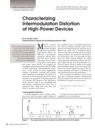
High-Power, High-Efficiency GaN HEMT Power ... - Cree, Inc.
High-Power, High-Efficiency GaN HEMT Power ... - Cree, Inc.
High-Power, High-Efficiency GaN HEMT Power ... - Cree, Inc.

You also want an ePaper? Increase the reach of your titles
YUMPU automatically turns print PDFs into web optimized ePapers that Google loves.
<strong>High</strong> Frequency Products<br />
4G AMPLIFIERS<br />
From May 2009 <strong>High</strong> Frequency Electronics<br />
Copyright © 2009 Summit Technical Media, LLC<br />
<strong>High</strong>-<strong>Power</strong>, <strong>High</strong>-<strong>Efficiency</strong><br />
<strong>GaN</strong> <strong>HEMT</strong> <strong>Power</strong> Amplifiers<br />
for 4G Applications<br />
By Simon Wood, Ray Pengelly, Don Farrell, and Carl Platis, <strong>Cree</strong>, <strong>Inc</strong>.,<br />
and Jim Crescenzi, Central Coast Microwave Design<br />
New <strong>GaN</strong> <strong>HEMT</strong> devices<br />
allow the design of high<br />
power amplifiers with the<br />
desired linearity and<br />
efficiency for 4G applications<br />
such as WiMAX,<br />
UMTS and WCDMA<br />
Today’s wireless system<br />
requirements<br />
demand increasing<br />
performance from power<br />
amplifiers. The higher<br />
gain and output power<br />
available from today’s<br />
transistors reduce the<br />
number of amplifier<br />
stages, and improved efficiency decreases system<br />
DC power requirements and generated<br />
heat. But at these higher power and efficiency<br />
levels, power amplifier linearity needs to meet<br />
or exceed the requirements of past systems.<br />
Gallium nitride (<strong>GaN</strong>) <strong>HEMT</strong> based power<br />
transistors offer an ideal technology solution<br />
for these amplifiers due to their exceptionally<br />
high operating power density. <strong>Cree</strong>’s <strong>GaN</strong><br />
<strong>HEMT</strong> devices deliver RF power densities as<br />
high as 8 W/mm [1] of gate periphery due to<br />
superior thermal properties provided by the<br />
silicon carbide substrates on which they are<br />
fabricated. This is of considerable advantage<br />
when compared with silicon substrates.<br />
This article details three amplifier designs<br />
that cover a variety of 4G frequency bands.<br />
The first two designs are 2 GHz Doherty<br />
amplifiers with capable peak output power of<br />
480 W employing the new CGH21240F or<br />
CGH25240F pre-matched <strong>GaN</strong> <strong>HEMT</strong> transistors.<br />
These transistors offer twice the peak<br />
power of previously released transistors,<br />
CGH21120F and CGH25120F, from <strong>Cree</strong> [2].<br />
Doherty amplifiers offer a unique solution for<br />
linear amplifiers since the efficiency is maintained<br />
at powers backed off from saturation.<br />
The third design is a 900 MHz 120 W saturated<br />
power design for lower frequency operation<br />
using the new CGH09120F broadband<br />
Parameter<br />
Requirement<br />
Operating Frequency 2.11-2.17 GHz<br />
Modulation Signal<br />
3GPP WCDMA<br />
Output <strong>Power</strong> (average) 80 watts<br />
Drain <strong>Efficiency</strong> 50%<br />
DPD corrected ACLR1 –50 dBc<br />
Table 1 · CDPA21480 design targets.<br />
(unmatched) transistor. Linearity of all three<br />
designs is maintained through the use of digital<br />
pre-distortion (DPD).<br />
UMTS 2.1 GHz Band 480 W Doherty<br />
Amplifier<br />
The objective of this work was to develop a<br />
practical Doherty amplifier with nominally<br />
480 watts of peak power that was capable of<br />
linear operation under the UMTS protocol<br />
(aided by pre-distortion). Table 1 shows the<br />
design targets for the CDPA21480.<br />
A two-way Doherty configuration was chosen,<br />
as shown in Figure 1. The input is first<br />
divided using a power divider with isolation<br />
between its outputs. In this case, we chose a<br />
Wilkinson 2-section divider with equal power<br />
split. An unequal power split may be preferred<br />
for applications with higher peak-to-average<br />
signals (WiMAX for example). The two amplifiers<br />
(carrier and peaking) are usually quite<br />
similar in terms of matching circuits (but not<br />
identical), and differ primarily in the gate<br />
bias. The carrier amplifier is biased “on” and<br />
provides gain at low input levels. The peaking<br />
amplifier is biased “off” in its quiescent state,<br />
and turns on only after the input signal<br />
increases in level. It supplies additional output<br />
power (as well as dynamic loading of the<br />
36 <strong>High</strong> Frequency Electronics
<strong>High</strong> Frequency Products<br />
4G AMPLIFIERS<br />
Figure 1 · Two-way Doherty amplifier block diagram.<br />
Figure 2 · Typical simulation of Doherty<br />
amplifier two-tone intermodulation rejection<br />
vs. input power.<br />
carrier amplifier) at high input signal levels. The “turnon”<br />
of the peaking amplifier is dependent on both input<br />
power level and gate bias voltage, which in turn influence<br />
low RF power efficiency and peak power capability of the<br />
total configuration.<br />
The design approach for this relatively high power<br />
Doherty design is an extension of that presented previously<br />
[3] for a WiMAX amplifier with 1/10 the output level.<br />
Of course, the main difference is in the choice of transistors—the<br />
<strong>Cree</strong> CGH21240F <strong>GaN</strong> <strong>HEMT</strong> in this case. This<br />
device has internal pre-matching (within the transistor<br />
package) to simplify input matching required on the PCB.<br />
Additionally, this transistor is capable of producing over<br />
240 W output when operated with a +28 V drain supply,<br />
with typical gain of 17 dB (Class A/B operation).<br />
The two fundamental considerations for each stage<br />
are the bias condition (biased on, or pinched off, and to<br />
what degree) and the fundamental and harmonic<br />
impedance terminations presented to the transistors.<br />
Our approach was to start with a nominal Class J design<br />
[4], in which the stand alone stage was optimized in a 50<br />
ohm environment. Then the biases were adjusted for carrier<br />
and peaking functions, and the stages were inserted<br />
into the Doherty configuration. Next, matching elements<br />
of each stage were modified to optimize the Doherty operation.<br />
The Doherty output network, specifically including<br />
the output offset lines, was also adjusted to maximize<br />
critical performance parameters.<br />
One challenging aspect of Doherty amplifier designs is<br />
that there are many variables to adjust [5, 6, 7]. These<br />
include, for example:<br />
1. Input divider coupling factor (equal in this case).<br />
2. Source impedance for both carrier and peaking<br />
amplifiers (including harmonics).<br />
3. Load impedance for both carrier and peaking amplifiers<br />
(including harmonics).<br />
4. Output offset line length.<br />
5. Quarter wave input and output line lengths (a quarter<br />
wave at the high end of the band in this case).<br />
6. Output transformer impedance.<br />
7. Carrier and peaking amplifier quiescent bias levels.<br />
The initial design approach involved considerable simulation<br />
while varying different circuit elements, to synthesize<br />
a solution that results in a near-optimum tradeoff<br />
of efficiency, linearity, and peak power. Linearity is simulated<br />
using two-tone CW signals (as a substitute for the<br />
more complex UMTS signal), with a target of achieving<br />
intermodulation product suppression better than –25 dBc<br />
(–30 dBc for the “hill”). An example of a two-tone IM rejection<br />
simulation is shown in Figure 2.<br />
It is particularly instructive to examine the input<br />
match conditions as they impact IM rejection, peak<br />
power, and efficiency. The Doherty amplifier was partitioned<br />
at the transistor gates and a simplified Doherty<br />
Figure 3 · Test input circuit for source-pull simulations<br />
of the Doherty amplifier.<br />
38 <strong>High</strong> Frequency Electronics
<strong>High</strong> Frequency Products<br />
4G AMPLIFIERS<br />
Figure 4 · Source pull of the Doherty peaking amplifier<br />
at two input power levels: (a) P in<br />
= +37 dBm. Peak<br />
power contours (blue, 0.5 dBm step per contour) and<br />
IM rejection (green, 1.5 dB per contour); (b) P in<br />
= +31<br />
dBm. IM rejection (green, 2 dB per contour) and efficiency<br />
(red, 0.5% per contour).<br />
Figure 5 · Simulation of Doherty amplifier two-tone IM<br />
rejection and DC-RF efficiency versus output power<br />
(while varying the output offset line length ±10<br />
degrees).<br />
Figure 6 · Photo of the CDPA21480 Doherty amplifier.<br />
Figure 7 · CDPA21480 simulated small signal response.<br />
input network was substituted, as shown in Figure 3.<br />
This test input schematic allows source-pull of the carrier<br />
and peaking amplifier stages in the Doherty configuration.<br />
Only one source-pull tuner is activated per simulation.<br />
Also, note that the ideal input divider assures isolation<br />
between the tuners. Source pull of the peaking amplifier<br />
for input levels (31 and 37 dBm) corresponding to peak<br />
output level and to back-off hill operation were conducted,<br />
with results shown in Figure 4.<br />
The contours of Figure 4 demonstrate the tradeoff in<br />
determining “optimum” input match for the peaking<br />
amplifier. The contours in Figure 4(a) show peak power<br />
and IM rejection for an input power of +37 dBm (per<br />
tone). This level corresponds to peak output of the<br />
Doherty, and the input impedance for highest power and<br />
IM rejection are similar (efficiency is also reasonable, at<br />
this high power). The contours in Figure 4(b) are for an<br />
input power that is reduced by 6 dB, and corresponds to<br />
the back-off hill IM region for the Doherty amplifier. In<br />
this case, the contours show an overlapping region for<br />
best efficiency and best IM rejection. It is important to<br />
note that the optimum impedance for the lower power<br />
level (hill region) is quite different than for the peak<br />
power case. These contours demonstrate a key aspect of<br />
Doherty amplifier design—namely that it is possible to<br />
trade off (through peaking amplifier input match)<br />
Doherty amplifier peak power for improved efficiency and<br />
linearity at backed off power levels (i.e., in a power region<br />
that will correspond to the average power of a communications<br />
signal with high peak-to-average ratio). Another<br />
important variable in this tradeoff process is the gate bias<br />
voltage for the peaking amplifier.<br />
A number of simulations while varying the output circuit<br />
elements were employed in the synthesis process.<br />
The tradeoffs associated with adjusting the output offset<br />
line lengths (see Fig. 1) are demonstrated by the simulations<br />
of Figure 5. The simulations provide the choice of an<br />
offset line length that supports –30 dBc hill IMD levels,<br />
while also achieving near optimum efficiency. .<br />
The emphasis on minimizing 2-tone IM distortion<br />
products while maintaining high efficiency and peak output<br />
capability was for the purpose of minimizing distortion<br />
under UMTS protocols. The basic assumption is that<br />
40 <strong>High</strong> Frequency Electronics
<strong>High</strong> Frequency Products<br />
4G AMPLIFIERS<br />
Figure 8 · Measured WCDMA transfer curves.<br />
Figure 9 · Single-carrier UMTS output spectrum (with<br />
and without predistortion).<br />
achieving a reasonably linear (uncorrected) amplifier will<br />
set the stage for highly linear operation when digital predistortion<br />
is applied. Our synthesis approach is critically<br />
dependent on the availability of good nonlinear transistor<br />
models, as is the case for the <strong>Cree</strong> <strong>GaN</strong> <strong>HEMT</strong> devices.<br />
These designs were thoroughly vetted using extensive<br />
simulations before any physical hardware was fabricated.<br />
The simulations were all performed using the AWR<br />
Microwave Office nonlinear simulator [8].<br />
Figure 6 shows the assembled version of the UMTS<br />
Doherty amplifier (the <strong>Cree</strong> CDPA21480). Figure 7 shows<br />
small signal simulation of the CDPA21480. The amplifier<br />
delivers greater than 14 dB power gain across the 2.11-<br />
2.17 GHz band. Figure 8 shows single-carrier WCDMA<br />
transfer curves with a 6.5 dB peak-to-average ratio (PAR)<br />
WCDMA signal (the nearly duplicate curves are for upper<br />
and lower adjacent channels). A digital pre-distortion<br />
(DPD) system as described in reference [3] was used to<br />
correct the linearity. The correction achieved for both single<br />
and two-channel WCDMA signals using predistortion<br />
is over 20 dB (Fig. 9 and Fig. 10), and well within the<br />
applicable standards. At the target 80 W average (singlechannel)<br />
output power the corrected ACLR1 is better<br />
than –50 dBc with 11 dB gain and 50% drain efficiency.<br />
<strong>Efficiency</strong> for the two-channel case exceeds 48% at 80 W<br />
average output.<br />
WiMAX 2.35 GHz 480 W Doherty Amplifier<br />
A second Doherty amplifier, the CDPA23480, provides<br />
50 W average power WiMAX performance at 2.35 GHz.<br />
This amplifier incorporates an internally matched input<br />
CGH25240 transistor designed to provide 240 W peak<br />
power from 2.30 to 2.70 GHz. CDPA23480 development<br />
followed an identical design path as the CDPA21480<br />
Doherty amplifier. Table 2 shows design targets for the<br />
CDPA23480 Doherty amplifier.<br />
Figure 10 · Two-carrier UMTS output spectrum (with<br />
and without predistortion).<br />
Detailed design of this amplifier used Microwave<br />
Office software with <strong>Cree</strong>’s large signal transistor model.<br />
Large signal simulations allowed for design trade-offs in<br />
the simulator to create an optimal design. Due to the<br />
higher PAR one trade-off considered was an unbalanced<br />
Doherty design [9] to improve linearity further than 6 dB<br />
back off. This approach was not pursued since directing<br />
more power to the peaker reduced the linear gain of the<br />
amplifier. Circuit simulation, tuning and optimization<br />
actually pushed the input balance more towards the carrier<br />
amplifier to improve gain and linearity. To allow<br />
Parameter<br />
Requirement<br />
Operating Frequency 2.30-2.40 GHz<br />
Modulation Signal 10 MHz wide WiMAX signal<br />
Output <strong>Power</strong> (average) 50 watts<br />
Drain <strong>Efficiency</strong> 40%<br />
DPD corrected SEM –45 dBc<br />
@ 6.5 MHz offset<br />
Table 2 · CDPA23480 design goals.<br />
42 <strong>High</strong> Frequency Electronics
<strong>High</strong> Frequency Products<br />
4G AMPLIFIERS<br />
Figure 11 · CDPA23480 AWR layout.<br />
Figure 12 · CDPA23480 simulated<br />
linearity results.<br />
Figure 14 · CDPA23480 simulated<br />
vs. measured responses.<br />
Figure 15 · Measured WiMAX transfer curves.<br />
Figure 13 · Photo of the CDPA23480 Doherty amplifier.<br />
design margin, the circuit was designed for 200 MHz<br />
bandwidth providing 50 MHz guard bands on each band<br />
edge. This wider bandwidth design goal sacrificed some<br />
optimal linearity and efficiency to hold uniform performance<br />
across the band. Experience shows that a –30 dBc<br />
two tone IMD3 design goal provides an amplifier DPD<br />
correctable to better than –45 dBc with a 802.16e WiMAX<br />
signal. Therefore the design target for simulated two tone<br />
IMD3 is –30 dBc. Figure 11 shows the Microwave Office<br />
layout of the simulated CDPA23480. Figure 12 shows<br />
simulated linearity from 2.25 to 2.45 GHz.<br />
Figure 13 shows the assembled version of the<br />
CDPA23480. Figure 14 shows measured small signal data<br />
of the CDPA23480 along with simulated results. Small<br />
signal correlation is excellent for this amplifier. Figure 15<br />
shows WiMAX transfer curves at 2.40 GHz with and<br />
without DPD correction. The 10MHz WiMAX signal corrects<br />
to –50 dBc at 50 W (47 dBm) with 39% drain efficiency.<br />
Measurements across the frequency band show<br />
similar results.<br />
LTE 870 MHz, 120 Watt Amplifier<br />
The <strong>GaN</strong> <strong>HEMT</strong> transistors used in the CDPA21480<br />
and 23480 power amplifiers have input pre-matching<br />
within the packages. The transistor used in the 900 MHz<br />
amplifier, which is the 120-watt peak power CGH09120F,<br />
has no internal pre-matching. This allows the device to be<br />
used over a wide range of applications at a variety of frequencies.<br />
The CGH09120F demonstration amplifier was<br />
designed, using <strong>Cree</strong>’s proprietary large-signal model, to<br />
have useful performance over 700 to 950 MHz. A summary<br />
of the design goals is shown in Table 3.<br />
The power amplifier was realized using a combination<br />
of microstrip and lumped element (shunt capacitor)<br />
matching. The topology used allows optimum performance<br />
to be achieved over frequencies anywhere between<br />
700 and 1600 MHz by adjusting the physical positions<br />
and values of the shunt capacitors. The amplifier<br />
described here was optimized for best performance<br />
around 870 MHz with the intention to exercise the circuit<br />
with LTE test signals when available. For the purposes of<br />
Parameter<br />
Requirement<br />
Operating Frequency 700 to 950 MHz<br />
Modulation signal 2-carrier W-CDMA with 10 MHz<br />
(for testing purposes) bandwidth and PAR of 7.5 dB<br />
Output <strong>Power</strong> (average) 20 watts<br />
Drain efficiency 35%<br />
DPD corrected ACLR1 –50 dBc<br />
Operating Voltage 28 volts<br />
Table 3 · CGH09120F demonstration amplifier design<br />
goals.<br />
44 <strong>High</strong> Frequency Electronics
<strong>High</strong> Frequency Products<br />
4G AMPLIFIERS<br />
Figure 16 · Photo of the CGH09120<br />
demonstration amplifier.<br />
this article the PA was tested with 2-<br />
carrier W-CDMA signals having a<br />
total PAR of 7.5 dB and channel<br />
bandwidths of 5 MHz.<br />
Figure 16 shows a photograph of<br />
the completed single-ended amplifier.<br />
The simulated small-signal S parameters<br />
of the design are shown in<br />
Figure 17 and large-signal parameters<br />
(gain, output power and drain<br />
efficiency) are shown in Figure 18.<br />
Measured peak power at 870 MHz<br />
was greater than 124 watts with a<br />
drain efficiency of 75%. This compares<br />
with a simulated peak output power<br />
of 134 watts and drain efficiency of<br />
81%. The broadband performance of<br />
the amplifier, over the 700 to 950<br />
MHz frequency range is shown in<br />
Figure 19. Saturated output power<br />
varies from 114 to 128 watts at drain<br />
efficiencies of 66 to 80% over 750 to<br />
950 MHz. Measured gain of the<br />
amplifier at 20 watts W-CDMA average<br />
output power is 21 dB with an<br />
accompanying drain efficiency of 35%<br />
and native ACLR1 of –36 dBc (in a<br />
5 MHz wide adjacent channel). Figure<br />
20 shows the 2 carrier W-CDMA spectral<br />
plots before and after DPD correction.<br />
Post DPD ACLR1 is –51 dBc<br />
at 20 watts average output power.<br />
Figure 17 · Simulated small-signal<br />
performance of the CGH09120F<br />
demonstration PA.<br />
Figure 19 · Measured broadband<br />
performance of CGH09120 PA.<br />
Summary and Conclusions<br />
This article has described the<br />
design of three power amplifiers for<br />
4G applications. Two Doherty designs<br />
employing the new CGH21240F and<br />
CGH25240F <strong>GaN</strong> <strong>HEMT</strong> transistors<br />
show exceptionally high efficiencies<br />
while maintaining the ability to be<br />
digitally pre-distorted to meet spectral<br />
mask requirements. A simpler<br />
Class A/B single stage power amplifier<br />
design using the new CGH09120F<br />
<strong>GaN</strong> <strong>HEMT</strong> transistor at 870 MHz<br />
has also been demonstrated.<br />
References<br />
1. Y.-F. Wu, A. Saxler, M. Moore, R.<br />
P. Smith, S. Sheppard, P. M.<br />
Chavarkar, T. Wisleder, U. K. Mishra,<br />
P. Parikh, “30-W/mm <strong>GaN</strong> <strong>HEMT</strong>s by<br />
field plate optimization,” IEEE<br />
Electron Device Lett., vol. 25, no. 11,<br />
pp. 117-119, Nov. 2004.<br />
2. Don Farrell, Jim Milligan, Brad<br />
Million, Ray Pengelly, Carl Platis, Bill<br />
Pribble, Peter Smith, Simon Wood,<br />
“Tracking Advances In <strong>High</strong>-<strong>Power</strong><br />
<strong>GaN</strong> <strong>HEMT</strong>s,” Microwaves and RF,<br />
Feb 2009.<br />
3. Simon Wood, Ray Pengelly, &<br />
Jim Crescenzi, “A <strong>High</strong> <strong>Efficiency</strong><br />
Doherty Amplifier with Digital<br />
Predistortion for WiMAX,” <strong>High</strong><br />
Frequency Electronics, Dec 2008.<br />
Figure 18 · Simulated large signal<br />
performance of the CGH09120F<br />
demonstration amplifier.<br />
Figure 20 · Pre and post spectral<br />
plots of CGH09120F demonstration<br />
amplifier.<br />
4. Steve C. Cripps, RF <strong>Power</strong><br />
Amplifiers for Wireless Communications,<br />
2nd ed., Artech House, 2006,<br />
pp. 68-73, 122-124<br />
5. R.S. Pengelly, “N-way RF power<br />
amplifier with increased back-off<br />
power and power added efficiency,”<br />
U.S. Patent 6,700,444, Mar. 2, 2004.<br />
6. R.S. Pengelly and S.M. Wood,<br />
“N-way RF power amplifier circuit<br />
with increased back-off capability<br />
and power-added efficiency using<br />
unequal input power division,” U.S.<br />
Patent 6,737,922, May 18, 2004.<br />
7. R.S. Pengelly and S.M. Wood,<br />
“N-way RF power amplifier circuit<br />
with increased back-off capability<br />
and power-added efficiency using<br />
selected phase lengths and output<br />
impedances,” U.S. Patent 6,791,417,<br />
Sep. 14, 2004.<br />
8. Microwave Office v8.05, AWR<br />
Corporation, El Segundo CA.<br />
9. M. Iwamoto, A. Williams, P.-F<br />
Chen, Andre G. Metzger, Lawrence E.<br />
46 <strong>High</strong> Frequency Electronics
Larson, Peter M. Asbeck, “An<br />
Extended Doherty Amplifier With<br />
<strong>High</strong> <strong>Efficiency</strong> Over a Wide <strong>Power</strong><br />
Range,” IEEE MTT, vol. 49 no. 12 pp.<br />
2472-2479, Dec 2001.<br />
Author Information<br />
Simon Wood has a Bachelor of<br />
Engineering degree from the<br />
University of Bradford, UK. Since<br />
joining <strong>Cree</strong> <strong>Inc</strong>. in 2000, he has<br />
designed amplifiers using SiC MES-<br />
FET, Si LDMOS, and more recently<br />
<strong>GaN</strong> <strong>HEMT</strong> devices. He has been<br />
Manager of Product Development at<br />
<strong>Cree</strong> since January 2006. He holds<br />
five United States patents in amplifier<br />
design. Simon can be reached at<br />
Simon_Wood@cree.com<br />
Ray Pengelly gained his BSc. and<br />
MSc. degrees from Southampton<br />
University, England in 1969 and<br />
1973, respectively. Since August<br />
1999, Ray has been employed by <strong>Cree</strong><br />
<strong>Inc</strong>. Initially, he was the General<br />
Manager for <strong>Cree</strong> Microwave responsible<br />
for bringing <strong>Cree</strong>’s wide<br />
bandgap transistor technology to the<br />
commercial marketplace. On the<br />
acquisition of UltraRF in 2001, he<br />
became Chief Technical Officer. From<br />
September 2005 he has been responsible<br />
for new business development of<br />
wide bandgap technologies for RF<br />
and microwave applications, most<br />
recently has been involved with the<br />
release of <strong>GaN</strong> <strong>HEMT</strong> transistors<br />
and ICs for general purpose and<br />
telecommunications applications.<br />
Jim Crescenzi received the BS<br />
degree at UC Berkeley in 1961 and<br />
the MS and PhD degrees at the<br />
University of Colorado in 1962 and<br />
1969. He founded Central Coast<br />
Microwave Design in 2005, where he<br />
provides consulting services primarily<br />
for microwave power amplifiers<br />
and subsystems. Jim is a Life Fellow<br />
of the IEEE for contributions to the<br />
development of microwave amplifiers,<br />
integrated circuit technology,<br />
and miniature receivers for defense<br />
applications. He can be reached at<br />
jcrescenzi@gmail.com.<br />
Don Farrell received his BSEE<br />
from Syracuse University (1984) and<br />
MSEE from The Johns Hopkins<br />
University (1988). Since 2006 Don<br />
has been working at <strong>Cree</strong> developing<br />
high power packaged <strong>GaN</strong> transistors<br />
and circuits. Don is a member of<br />
IEEE and has authored numerous<br />
magazine articles and papers.<br />
Carl Platis is a Test Engineer at<br />
<strong>Cree</strong>, <strong>Inc</strong>. since May 2007. He has<br />
specialized in RADAR and<br />
Microwave technology for 27 years at<br />
Naval Air Systems Command, Naval<br />
Research Laboratory and United<br />
States Navy. He received an ASET<br />
degree from Capitol College, Laurel<br />
Maryland in 1995. He is a 27 year<br />
military veteran currently serving in<br />
the United States Coast Guard<br />
Selected Reserve.