Embedded Wafer-Level-Packages - I-Micronews
Embedded Wafer-Level-Packages - I-Micronews
Embedded Wafer-Level-Packages - I-Micronews
You also want an ePaper? Increase the reach of your titles
YUMPU automatically turns print PDFs into web optimized ePapers that Google loves.
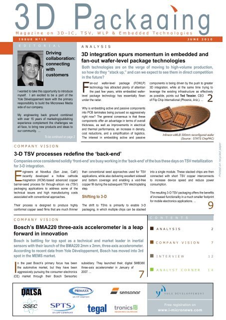
Magazine on 3D-IC, TSV, WLP & <strong>Embedded</strong> Technologies<br />
ISSUE n°15 JUNE 2010<br />
e d i t o r i a l ANALYSIS<br />
Driving<br />
collaboration:<br />
connecting<br />
with<br />
customers<br />
I wanted to take this opportunity to introduce<br />
myself. I am excited to be a part of the<br />
Yole Développement team with the primary<br />
responsibility to build the <strong>Micronews</strong> Media<br />
side of our company.<br />
My engineering back ground combined<br />
with over 15 years of marketing/publishing<br />
experience complement the challenges we<br />
all face, to bring new products and ideas to<br />
our community. ...<br />
To be continued on page 2<br />
3D integration spurs momentum in embedded and<br />
fan-out wafer-level package technologies<br />
Both technologies are on the verge of moving to high-volume production,<br />
so how do they “stack up,” and can we expect to see them in direct competition<br />
in the future?<br />
Fan-out wafer-level package (FOWLP)<br />
technology has attracted plenty of attention<br />
the past few years, while embedded waferlevel<br />
package technology has essentially flown<br />
under the radar.<br />
Why is embedding active and passive components<br />
into PCB laminates being pursued so aggressively<br />
right now? The general consensus is that these<br />
components offer an advantage in terms of overall<br />
thickness, as well as improvements in electrical<br />
and thermal performance, an increase in density,<br />
cost reductions, and a simplification of logistics.<br />
The interest in embedding active and passive<br />
components is being driven by the push to greater<br />
3D integration, while at the same time trying to<br />
leverage the existing infrastructure as effectively<br />
as possible, points out Ted Tessier, CEO<br />
of Flip Chip International (Phoenix, Ariz.). ...<br />
2<br />
Infineon eWLB 300mm reconfigured wafer<br />
(Source : STATS ChipPAC)<br />
COMPANY vision<br />
3-D TSV processes redefine the ‘back-end’<br />
Companies once considered solidly ‘front-end’ are busy working in the ‘back-end’ of the bus these days on TSV metallization<br />
for 3-D integration.<br />
Engineers at Novellus (San Jose, Calif.)<br />
recently developed a hollow cathode<br />
magnetron (HCM)-based advanced copper<br />
barrier-seed process for through-silicon via (TSV)<br />
packaging applications to address some of the<br />
technical issues and high manufacturing costs<br />
associated with conventional approaches.<br />
Their process is designed to produce highly<br />
conformal copper seed films that are much thinner<br />
than conventional seed approaches used for TSV<br />
applications, while also delivering excellent sidewall<br />
and bottom coverage and enabling a void-free<br />
copper fill during the subsequent TSV electroplating<br />
step.<br />
Shifting to 3-D<br />
The shift to TSVs is primarily to enable 3-D<br />
packaging, in which multiple chips can be stacked<br />
into a single module. These stacked chips are then<br />
connected with short TSV copper interconnects<br />
to increase device speed and reduce power<br />
consumption.<br />
The resulting 3-D TSV packaging offers the benefits<br />
of increased functionality in a much smaller footprint<br />
for mobile electronics applications. ...<br />
9<br />
Printed on recycled paper<br />
COMPANY vision<br />
Bosch’s BMA220 three-axis accelerometer is a leap<br />
forward in innovation<br />
Bosch is battling for top spot as a technical and market leader in inertial<br />
sensors with their launch of the BMA220 2mm x 2mm, three-axis accelerometer.<br />
According to recent data from Yole Développement, Bosch has moved into 3rd<br />
spot in the MEMS market.<br />
C O N T E N T S<br />
ANALYSIS 2<br />
COMPANY vision 7<br />
INTERVIEW 12<br />
In the past Bosch’s primary focus has been<br />
the automotive market, but they have been<br />
aggressively pursuing the consumer electronics<br />
(CE) market through their Bosch Sensortec<br />
subsidiary. They launched their, digital SMB380<br />
three-axis accelerometer in January of<br />
2007. ...<br />
7<br />
ANALYST CORNER 14<br />
Free registration on<br />
www.i-micronews.com
JUNE 2010 issue n°15<br />
Newsletter on 3D IC, TSV, WLP & <strong>Embedded</strong> Technologies<br />
E D I T O R I A L<br />
<strong>Micronews</strong> Media has been producing and<br />
will continue to produce valuable information<br />
(content) to the wafer microelectronic<br />
manufacturing market place. In fact, it’s one<br />
of the only sources analyzing and reporting<br />
all of technologies together under one wafer!<br />
For example, in this issue Jérôme Baron<br />
has in depth analysis of FOWLP conducting<br />
exclusive high level interviews while at the<br />
same time providing a road map to where<br />
it is all heading! New subscribers join our<br />
community every day, and almost all of you<br />
say you want to stay informed on usually<br />
more than 3 technologies. To help you stay<br />
current and ahead of your competition, we<br />
deliver magazines 30 times a year packed<br />
full of analysis and information plus our<br />
website has exclusive content every day. You<br />
should also feel confident that your peers,<br />
our subscribers, are the key decision makers<br />
from this industry including executives,<br />
engineers, marketers, biz development,<br />
R&D department and more, representing the<br />
drivers of this fast moving marketplace.<br />
a n a l y s i s<br />
3D integration spurs momentum in<br />
embedded and fan-out wafer-level<br />
package technologies<br />
From page 1<br />
“From a reliability standpoint, embedded die<br />
components show absolutely outstanding<br />
mechanical robustness — even in drop tests.<br />
Embedding active devices into PCBs provides an<br />
alternative to wafer-level fan-out WLSCP or BGA<br />
applications,” he says.<br />
“Electrical performance is the primary driver and<br />
benefit,” says Lee Smith, vice president of product<br />
marketing at Amkor Technology (Chandler, Ariz.).<br />
“Form factor is another driver, but typically it’s<br />
applications such as DDR4, where the electrical<br />
limitations of wirebond window BGAs may be<br />
reaching their practical limits.”<br />
How will the technology start out? “First, simple<br />
small dies with low pin-count will be embedded in<br />
motherboards, such as integrated passive dies, in<br />
mobile applications,” explains Caroline Beelen-<br />
Hendrikx, director of strategy, operations backend<br />
innovation at NXP (Nijmegen, The Netherlands).<br />
She anticipates more complicated, larger dies will<br />
only be embedded in module or package interposer<br />
“First, simple small dies with low pin-count will be embedded in<br />
motherboards,” explains Caroline Beelen-Hendrikx, NXP<br />
Part of my job will be to help you develop<br />
marketing programs and ideas with the goal<br />
of educating and meeting our subscribers<br />
across the world. We are all partners helping<br />
to grow a very important industry driven by<br />
technology and innovation.<br />
Please call or email me with any questions<br />
or ideas. I look forward to meeting you and<br />
hearing from you soon!<br />
Bill Stinson<br />
VP New Media Development, Yole Inc.<br />
stinson@i-micronews.com<br />
e v e n t s<br />
• <strong>Embedded</strong> <strong>Wafer</strong> <strong>Level</strong> Packaging<br />
Workshop, Minatec Crossroads,<br />
June 24, Grenoble, France<br />
• SEMICON West,<br />
July 13-15, San Francisco, CA<br />
• SEMICON Taiwan,<br />
September 8-10, Taipei, Taiwan<br />
• ESTC - Electronics System Integration<br />
Technology Conference,<br />
September 13-16, Berlin, Germany<br />
secondary or coupled with electrical performance<br />
as to why to embed vs. other integration options.”<br />
Echoing industry consensus, Imbera Corp.’s<br />
(Melbourne, Fla.) Risto Tuominen, chief<br />
technology officer, and Jeff Baloun, CEO, report<br />
that the primary goals of most programs they’re<br />
involved with today are miniaturization, product<br />
design flexibility, and cost.<br />
Applications and markets<br />
For now, the applications and markets for the two<br />
technologies are different.<br />
<strong>Embedded</strong><br />
For embedded technology, the end markets<br />
and applications tend to be primarily consumer<br />
electronics and mobile ones.<br />
“Following the trail blazed by cellular volumes,<br />
it’s expected that the eventual adoption of these<br />
technologies for high-performance applications<br />
as possible alternatives to flip chip BGAs for<br />
microcontrollers and high-performance memory<br />
packaging applications will occur,” says Tessier.<br />
“<strong>Embedded</strong> die memory packaging will also be<br />
the next trend for high-performance computing<br />
boards, beginning with mobile products for which<br />
miniaturization is critical. And she won’t be surprised<br />
to see memory die embedded in a BGA interposer<br />
for improved electrical performance. Beelen-<br />
Hendrikx notes that embedding as a method to<br />
make a package is also possible, but yield is a big<br />
concern.<br />
Smith expects to see the technology in applications<br />
such as RF modules, graphic processors, FPGA,<br />
CPU, and high-performance ASICs.<br />
Werner Klingenstein, director of technology<br />
strategy at Infineon Technologies AG (Neubiberg,<br />
Germany), predicts that applications will encompass<br />
power supply, telecommunications, RF ID — with<br />
ramp-up of production beginning in 2011.<br />
And Imbera is already in small-volume production<br />
today, with significant growth forecasted for the<br />
beginning of Q4 2010 through 2011.<br />
FOWLP<br />
Fan-out wafer-level package (FOWLP) technology<br />
has been pursued more publicly, albeit every bit as<br />
aggressively.<br />
The primary drivers Seung Wook Yoon, deputy<br />
director of technology marketing at STATS ChipPAC<br />
Issue sponsored by:<br />
More information on page 15<br />
<strong>Embedded</strong> WLP fan-out package cross-section (Courtesy of Imbera)<br />
2
JUNE 2010 issue n°15<br />
Newsletter on 3D IC, TSV, WLP & <strong>Embedded</strong> Technologies<br />
Imbera embedded die packages (Courtesy of Imbera)<br />
(Singapore), cites are demand for thinner and<br />
smaller package solutions, especially for mobile<br />
applications; requirements for a robust package<br />
with copper and low-k compatibility, and lead-free/<br />
halogen-free, green material sets; proven lowercost<br />
path using a batch process and simplified<br />
supply chain; extendibility of the technology for<br />
device integration; and eliminating the substrate<br />
and bumping that serves to simplify logistics and<br />
the supply chain.<br />
FOWLP has a reputation as being a very expensive<br />
technology, due to the need for serial die processing<br />
into reconstructed wafers. And the infrastructure<br />
needed to support FOWLP in high-volume is much<br />
like a wafer fab or bump fab technology that’s more<br />
expensive than a laminate alternative, explains<br />
Tessier. “FOWLP is believed by some to be a good<br />
option where I/O count and die size constraints<br />
of some potential WLCSP applications result in<br />
package pitches that are finer than end-users can<br />
use in surface mount assembly processes with<br />
high yields. Only a narrow range of applications<br />
fall into the ‘sweet spot’ of FOWLP and, as a result,<br />
it’s expected to find limited usefulness. FOWLP is<br />
in direct competition with a number of conventional<br />
array packaging options, including flip chip CSPs.<br />
The interest in FOWLP is being driven by form<br />
factor without any consideration to the cost of this<br />
technology relative to other comparable packaging<br />
alternatives,” he adds.<br />
Aggressive players<br />
There are many companies making bold moves in<br />
the embedded space, including IDMs and fabless<br />
design houses. The SiP fabless segment, notably,<br />
appears to be leading at the moment.<br />
FOWLP is seeing certain companies emerge as<br />
“big players” as well.<br />
<strong>Embedded</strong><br />
In Japan, Ibiden and Casio are working within a<br />
powerful industry consortium to put in place the<br />
infrastructure to enable embedded component<br />
packaging technologies for cellular and consumer<br />
product applications, points out Tessier. “The<br />
Hermes consortia in Europe, led by AT&S (Austria)<br />
and the Fraunhofer Institute (Germany), as well<br />
as a number of industry leaders, is driving the<br />
establishment of a robust infrastructure in Europe.<br />
In Asia, SEMCO and Imbera, to name a few, are<br />
also helping to drive this revolution in 3D packaging,”<br />
he says. “In the area of embeddable components,<br />
NXP has been an industry leader among IC<br />
manufacturing companies. We’ve been supporting<br />
NXP’s vision, as well as using our single- and multilayer<br />
redistribution layer (RDL) technologies to<br />
enable the relaxation of embedded die packaging<br />
requirements.”<br />
FOWLP<br />
Infineon and its partners (STATS ChipPAC,<br />
STMicroelectronics, and ASE) are moving the most<br />
boldly with FOWLP technology.<br />
With its eWLB technology, Infineon is the<br />
acknowledged trendsetter in the industry. “Other<br />
companies who bought technology licenses (ASE,<br />
STATS ChipPAC, ST, and more coming soon), have<br />
set up substantial production capacities,” says<br />
Klingenstein.<br />
Through its partnership with Infineon, STATS<br />
ChipPAC ramped its first-generation eWLB<br />
Cross-Sectional View of an embedded die in printed wiring board fan-out interconnect (Courtesy of FlipChip)<br />
technology to high-volume production in the third<br />
quarter of 2009. “Current shipments are in excess<br />
of 30,000 reconstituted wafers per quarter,” notes<br />
Yoon. “While the rapid volume production ramp<br />
has taken place within a 200mm reconstituted<br />
wafer manufacturing process, we moved to a<br />
300mm reconstituted wafer manufacturing process<br />
to expand capacity and to realize a lower cost<br />
structure through the economy of scale.”<br />
And with the recent resolution of Freescale’s<br />
(Austin, Texas) and Epic Technologies’ (Woburn,<br />
Mass) intellectual property dispute in this space<br />
involving their RCP and ChipsFirst technologies,<br />
there’s an alternative technology source for FOWLP<br />
technology, as Tessier points out.<br />
Which current packages might the<br />
technologies replace?<br />
Between the two technologies, they’ll provide<br />
alternatives to many popular packages.<br />
<strong>Embedded</strong><br />
The general expectation is that embedded<br />
technology may replace or compete with 3D<br />
packages ranging from stacked die and stacked<br />
packages. While it might not actually “replace”<br />
a package, it can replace the practice of external<br />
mounting of passives or die with the embedding<br />
process at the substrate manufacturing stage.<br />
Tessier expects embedded component technology<br />
packages to displace reconstructed waferbased<br />
fan-out WLCSP technologies. Despite the<br />
industry’s current preoccupation with TSV-based<br />
3D packaging solutions, he thinks embedded<br />
component technology provides a highly<br />
practical packaging alternative with comparable<br />
density potential, while avoiding the logistical<br />
nightmares inherent in most TSV-based packaging<br />
alternatives. “<strong>Embedded</strong> die applications also<br />
provide alternatives to flip chip BGA applications<br />
involving copper low-k and other fragile package<br />
constructions that generally don’t do well in thermal<br />
cycling and mechanical stressing,” he says.<br />
3
JUNE 2010 issue n°15<br />
Newsletter on 3D IC, TSV, WLP & <strong>Embedded</strong> Technologies<br />
A limitation with embedding, beside yield, is still the<br />
bond pad pitch that can be handled. “So it will be<br />
low and medium pin-count packages, not high pincount<br />
BGAs. Cost and yield will determine which<br />
packages will be replaced,” says Beelen-Hendrikx.<br />
Tuominen and Baloun note that embedding is a<br />
subset to many of the package solutions today. In<br />
embedded BGA or SiP with embedded, the die is<br />
typically facing down, representing flip chip. If it’s<br />
possible to design your product into a WLP, then<br />
the embedded solution will become a secondary<br />
choice, they say, although we have reached<br />
physical limits that embedding can solve without<br />
too great of a cost overhead penalty. They expect<br />
typical wirebond products may see diminished<br />
growth as a result of embedding, but believe the<br />
package families themselves will continue with the<br />
compliment of embedded.<br />
FOWLP<br />
The general consensus is that based on its highperformance,<br />
small footprint, and lower cost<br />
structure, FOWLP could potentially replace flip chip<br />
FBGA and flip chip CSP packaging in the near-term<br />
and wirebond packages such as FBGA over the<br />
longer-term. With volume and cost erosion, FOWLP<br />
may also replace QFN for applications that don’t<br />
have stringent power dissipation requirements.<br />
Supply chain challenges<br />
First eWLB package was found in a LG cell-phone (Courtesy of SystemPlus Consulting)<br />
need to share a greater portion of the value-add<br />
with the high-density PCB suppliers that enable<br />
the high-density array packaging that will be used<br />
in the industry going forward, says Tessier. “Yield<br />
considerations are always a major concern in<br />
‘chips-first’ embedded component technologies,”<br />
he adds. “The infrastructure developed to provide<br />
known good WLCSPs will be leveraged to provide<br />
the high levels of die quality required to enable<br />
embedded die packaging with the yields needed to<br />
enable viable and cost-effective alternatives.”<br />
And another key point, according to Beelen-<br />
Hendrikx, is that now PCB manufacturers will<br />
be placing and interconnecting dies. The board<br />
manufacturer will also do final test. She believes<br />
this may result in issues with respect to the<br />
responsibilities of failures, both zero-hour and<br />
in the field. Also, semiconductor companies will<br />
have to disclose the final test program to the PCB<br />
manufacturer, which isn’t currently the case for<br />
chip-last technologies, in which the semiconductor<br />
manufacturer does the die placement, interconnect,<br />
and testing.<br />
FOWLP<br />
Since FOWLP doesn’t require substrates or<br />
bumping, it has a simplified logistics and supply<br />
chain structure.<br />
Beelen-Hendrikx points out that while there aren’t<br />
a lot of supply chain issues for FOWLP, proving<br />
high yield is still a problem and the reason for the<br />
high cost associated with the technology. “Yield is<br />
hampered, for example, by die shift during curing<br />
of the molding compound and warpage of the<br />
reconfigured wafer. Board-level reliability is an<br />
issue for larger packages,” she adds.<br />
Positioning embedded die vs. FOWLP<br />
In theory, embedded die can replace the same<br />
segment of products as FOWLP. The challenges<br />
faced by the two packaging schemes are the same:<br />
proving yield. “The consequences of the underlying<br />
two different infrastructures can be very different,”<br />
Yoon explains. “<strong>Embedded</strong> die using an existing<br />
PCB infrastructure has an advantage of cheaper<br />
capital, but also faces a severe yield challenge. The<br />
yield of manufacturing a 20-50µm feature (line and<br />
space) alone (without die) ranges from 70 to 95%.<br />
The goal is to achieve yields greater than 99% for<br />
a 10µm feature with die using a technology that is<br />
essentially already mature. The envelope is pushed<br />
beyond its limit here. FOWLP technology, on the<br />
other hand, uses a µm to sub-µm proven thinfilm<br />
technology infrastructure to generate a 10µm<br />
feature. Thus, yield is less of a challenge. Cost is a<br />
bigger challenge, since the equipment set is more<br />
expensive. The real challenge is achieving a rapid<br />
transition to a larger panel (300mm and beyond).”<br />
Yoon also believes it’s likely that embedded die will<br />
start with very simple, low pin-count devices to be<br />
embedded due to the severe challenge in yield. As a<br />
“<strong>Embedded</strong> die using an existing PCB infrastructure has an<br />
advantage of cheaper capital, but also faces a severe yield<br />
challenge”, explains Seung Wook Yoon, STATS ChipPAC<br />
result, these two package technologies may end up<br />
finding applications in different market segments.<br />
FOWLP, being an inherently more scalable<br />
technology, will find use in a wider spectrum of<br />
applications vs. embedded die, which is likely to<br />
remain a niche application — at least in the near<br />
future.<br />
4<br />
<strong>Embedded</strong><br />
There are many challenges ahead with the supply<br />
chain for embedded technology, primarily because<br />
one hasn’t been established with clear ownership<br />
yet.<br />
SATS companies that have historically been privy<br />
to the majority of the value-add associated with<br />
semiconductor packaging will be under pressure<br />
to share a greater portion of this value-add with<br />
high-density array packaging, which will also<br />
To successfully compete against existing packaging<br />
technologies, Tuominen and Baloun say the<br />
embedding supply chain needs to be highly integrated<br />
to provide a sufficient production lead-time and costeffective<br />
manufacturing solution. Imbera’s approach<br />
is to focus on the consolidation of the whole value<br />
chain. Further integration is needed in the area of<br />
RDL and backend processes, they note.<br />
The bottom line is that many questions related to<br />
the supply chain, such as “who’s doing what,” still<br />
require answers, says Klingenstein.<br />
Optical micrograph of NXP EMBIDS<br />
Daisy chain test vehicle
AT&S AG<br />
ECP ® - <strong>Embedded</strong> Component Packaging Technology<br />
Newsletter on 3D IC, TSV, WLP & <strong>Embedded</strong> Technologies<br />
JUNE 2010 issue n°15<br />
AT&S introduces the industry standard for embedding of active and discrete passive components inside a printed circuit<br />
board. ECP ® (<strong>Embedded</strong> Component Packaging) offers the most reliable chip embedding solution based on qualified<br />
processes validated to the highest quality standards in the industry.<br />
ECP ® is a highly efficient technology which benefits a broad application range, from single chip modules and printed circuit<br />
boards with several embedded passives up to high complexity System-in-Package modules and System-in-Board applications.<br />
PCB and SiB Applications<br />
ECP ® releases surface space for other components<br />
or allows the overall PCB size to be reduced<br />
Highly Reliable PCB for Harsh Conditions<br />
Car Engine Control PCB<br />
PCB for Portable Music Player<br />
Notebook and Netbook PCB<br />
PCB for Mobile Internet Devices<br />
PCB for Digital Cameras<br />
Mobile Modem Boards<br />
Mobile Phone Boards<br />
Hearing Aid PCB<br />
Integrated RFID<br />
Single Chip and SiP Modules<br />
ECP ® represents a powerful alternative for existing<br />
packaging types and enables advanced 3D packaging<br />
concepts<br />
ESD / EMI Protection Networks<br />
Power MosFet<br />
Power Modules<br />
MEMS Modules<br />
Sensor Modules<br />
RFID Modules<br />
Radio Modules<br />
Camera Modules<br />
IC Drivers<br />
Audio Modules<br />
DC/DC Converters<br />
By using the ECP ® technology, electronic products can be miniaturised efficiently while providing a whole feature-set to<br />
increase the overall performance of your application.<br />
Miniaturisation in xy dimensions and in thickness<br />
Integration of active and discrete passive components<br />
Enhanced mechanical reliability and stability by<br />
avoiding soldering between component and substrate<br />
Improved electrical performance and better thermal<br />
performance through short signal paths<br />
High flexibility in design by enabling 3D routing from<br />
front to back side of embedded components<br />
Advanced packaging capability: 3D stacking in<br />
package and stacking of packaged ICs<br />
Cost efficiency by using a large production format<br />
(18” x 24”) and substituting gold bonding with<br />
galvanic interconnection<br />
Nikolai Haslebner<br />
Product Manager<br />
Business Line Advanced Packaging<br />
e-mail: n.haslebner@ats.net<br />
AT&S AG<br />
Fabriksgasse 13<br />
8700 Leoben, Austria<br />
www.ats.net<br />
® Registered Trademark AT 255868<br />
5
JUNE 2010 issue n°15<br />
Newsletter on 3D IC, TSV, WLP & <strong>Embedded</strong> Technologies<br />
Due to the robust infrastructure in place for laminatebased<br />
embedded die technologies, Tessier expects<br />
embedded die technologies will capture the lion’s<br />
share of 3D applications in that space.<br />
Some applications may be the same, Tuominen and<br />
Baloun say, although the embedded die application<br />
area is wider and the I/O range is probably also<br />
wider. Further, they firmly believe 2nd-gen FOWLP will<br />
develop the technology closer to the embedded die.<br />
And Klingenstein expects embedded die technology<br />
to find its niche in applications that don’t require fine<br />
pitches or high accuracy.<br />
Will the two technologies compete<br />
in the long-term (after 2013), when<br />
FOWLP 2nd-gen with TMV arrive, and<br />
FOWLP also shifts to 3D?<br />
Tessier expects laminate-based embedded die<br />
to win out both in the mid-term and long-term,<br />
thanks to an existing infrastructure that can support<br />
widespread adoption of the technology. “The<br />
evolution of packaging solutions to incorporate TMV<br />
advancements is more readily applicable to laminatebased<br />
solutions. It appears embedded die options<br />
will benefit most from TMV technologies,” he says.<br />
The most important objective for the technologies,<br />
according to Tuominen and Baloun, is to be<br />
technically competitive and cost-effective compared<br />
to existing packaging technologies. Both embedded<br />
die and FOWLP technologies will be further<br />
developed to meet these needs, they say.<br />
Long-term competitiveness comes from the timing<br />
of a credible manufacturing infrastructure, Yoon<br />
points out. <strong>Embedded</strong> die technology must prove<br />
itself within a year or so, he says, or it’s likely to<br />
remain a niche technology at best.<br />
And ultimately, as Beelen-Hendrikx notes,<br />
whichever technology can deliver the lowest<br />
cost and highest yield with acceptable reliability<br />
performance will eventually win out.<br />
3D Packaging Tool-Box<br />
Sally Cole Johnson for Yole Développement<br />
It’s entirely possible, but we’ll have to wait and see<br />
because opinions vary greatly.<br />
It’s difficult to envision 2nd-generation FOWLP with<br />
TMV as cost-effective as package-on-package<br />
(PoP) technology, says Smith. «<strong>Embedded</strong> die and<br />
top components must be designed so that there’s<br />
only one RDL per side, and small package sizes, to<br />
end up with a high number of die per rebuilt wafer,»<br />
he adds. “There may be niche applications for the<br />
technology, but for the mainstream, baseband<br />
processor, and combination memory applications<br />
in smartphones that PoP serves, FOWLP can’t<br />
cost-effectively handle the interconnect density<br />
requirements and package size range.”<br />
Source : Yole Développement, <strong>Embedded</strong> WLP – 2010 Report<br />
Jeff Baloun, managing director<br />
and CEO of Imbera Corp., has<br />
more than 25 years’ semiconductor<br />
manufacturing experience. He<br />
holds a B.S. degree in computer<br />
science-business from the Florida<br />
Institute of Technology.<br />
Caroline Beelen-Hendrikx,<br />
director of strategy, operations<br />
backend innovation at NXP, is<br />
responsible for the semiconductor<br />
packaging roadmap. She has 18<br />
years’ experience in electronics<br />
packaging and assembly at Philips<br />
and NXP as a process engineer and development<br />
manager.<br />
Werner Klingenstein, Ph.D.,<br />
is the director of technology<br />
strategy at Infineon Technologies<br />
AG. He began his career with<br />
wafer technology development<br />
at Siemens Semiconductor,<br />
focusing on CMOS and EEPROM<br />
devices. He later spent 2 years on assignment<br />
in the U.S. working on DRAM wafer technology<br />
development and design interface. For the past<br />
13 years, Klingenstein has worked for the strategy<br />
department with a focus on technology screening<br />
and evaluation. He specializes in advanced MEMS<br />
and packaging technologies.<br />
Lee Smith is vice president<br />
of product marketing at Amkor<br />
Technology. He’s an industry<br />
expert in 3D packaging, with nearly<br />
30 years of diverse technology and<br />
market development experience.<br />
Ted Tessier is the chief technical<br />
officer at FlipChip International. He<br />
has more than 25 years’ experience<br />
in the semiconductor packaging<br />
industry and a comprehensive<br />
industry perspective, based<br />
on senior engineering and<br />
management positions at Nortel, Motorola,<br />
Biotronik, Amkor, STATS ChipPAC, and FCI. He has<br />
published actively and is well known in the industry<br />
for his work in the areas of advanced packaging<br />
technologies, including wafer bumping, multichip<br />
modules/system-in-package technologies, flip<br />
chips, 3D packaging, WLSCPs, and wafer-level<br />
processes.<br />
Risto Tuominen, chief technology<br />
officer at Imbera Corp., is responsible<br />
for technology licensing, technology<br />
roadmaps, R&D, development,<br />
adoption, and ramp-up to high volume.<br />
He graduated with a M.S. from Helsinki<br />
University of Technology. His major<br />
was Electronics Production Technology, and for his<br />
thesis he developed the first integrated module board<br />
technology generation. He later launched Imbera and<br />
served as CEO.<br />
Seung Wook Yoon, Ph.D., MBA,<br />
deputy director of technology<br />
marketing at STATS ChipPAC, is<br />
in charge of technology marketing<br />
of next-generation integration<br />
technology, including TSVs,<br />
embedded packaging, integrated<br />
passive device, and 3-D IC packaging. Prior to<br />
joining STATS ChipPAC, he was deputy lab director<br />
of the Microsystem, Module, and Components Lab<br />
at the Institute of Microelectronics in Singapore.<br />
Yoon received a Ph.D. in materials science and<br />
engineering in 1998 from KAIST in Korea. He also<br />
holds an MBA from Nanyang Business School in<br />
Singapore. He has authored more than 80 journal and<br />
conference papers, and holds several U.S. patents on<br />
microelectronic materials and electronic packaging.<br />
6
JUNE 2010 issue n°15<br />
Newsletter on 3D IC, TSV, WLP & <strong>Embedded</strong> Technologies<br />
c o m p a n y v i s i o n<br />
Bosch’s BMA220 three-axis accelerometer<br />
is a leap forward in innovation<br />
From page 1<br />
This was the first three-axis acceleration<br />
sensor to be offered in a 3 mm x 3 mm x 0.9<br />
mm plastic package; however, within less than<br />
two years all their major competitors, including<br />
STMicroelectronics, Freescale, Analog Devices<br />
and Kionix, were offering similar 3 mm x 3 mm<br />
products targeted at the CE market. Chipworks<br />
provided a review of these products in a recent<br />
article in Yole I-<strong>Micronews</strong>.<br />
In late 2007, Chipworks completed a detailed<br />
structural analysis of the SMB380. This was<br />
followed by a circuit analysis of the ASIC. The<br />
structural analysis found that the SMB380 was<br />
fabricated using separate ASIC and MEMS devices<br />
mounted side-by-side in the plastic QFN package.<br />
The MEMS die was formed using a three-poly,<br />
DRIE surface micromachining (“Bosch-etch”)<br />
process. The MEMS structure showed completely<br />
independent capacitive sensors for X, Y and Z<br />
acceleration. The poly 3 used to form the movable<br />
structures was the thickest we had seen at that<br />
time.<br />
Since the launch of the SMB380, Bosch has<br />
released a number of other 3 mm x 3 mm<br />
accelerometers, including the BMA140 and<br />
BMA150 in LGA packages, which Chipworks has<br />
found are based on essentially the same MEMS die<br />
technology as the SMB380. The analog BMA140<br />
uses a different ASIC, while the digital BMA150<br />
uses the same ASIC as the SMB380. Chipworks<br />
has seen the BMA150 (usually unbranded) in a<br />
Figure 2: Tilt-View SEM Micrograph of BMA220<br />
MEMS Structure (Courtesy of Chipworks)<br />
Figure 3: BMA 220 X-ray side<br />
(Courtesy of Chipworks)<br />
variety of CE products, including most recently<br />
the Google Nexus One smart phone. As an aside,<br />
STMicroelectronics continues to win sockets in<br />
Apple products, including the recent design win for<br />
the LIS331DLH accelerometer in the new iPad. In<br />
January of 2010 Bosch has once again leapt ahead<br />
of the competition with the BMA220, which comes<br />
in an LGA plastic package.<br />
At Chipworks, we were very curious to find out how<br />
Bosch had achieved the smaller package size used<br />
for the BMA220. Our article in Yole I-<strong>Micronews</strong><br />
speculated that Bosch could have achieved a 2.4<br />
mm x 2.4 mm package with the SMB380 MEMS<br />
and ASIC chips if they adopted the stacked<br />
geometry used by STMicroelectronics. This would<br />
have required thinning the ASIC die, and perhaps<br />
the MEMS die, to keep the thickness below 1 mm.<br />
Chipworks has procured samples of the BMA220<br />
and our analysis has confirmed that Bosch had<br />
indeed moved to a stacked geometry for the<br />
BMA220. They also needed to shrink the chip sizes<br />
and the ASIC thickness. A tilt-view SEM, which<br />
reveals the internal structure of the BMA220, is<br />
presented in Figure 2.<br />
The BMA220 is a disruptive, market leading<br />
innovation from Bosch. The competition for inertial<br />
sensor sockets in CE devices is fierce. Printed<br />
circuit board space is at a premium in CE products,<br />
and so we can expect their competitors to respond<br />
aggressively. STMicroelectronics is presently<br />
Figure 1: Decapsulated BMA220 MEMS and ASIC Chips (Courtesy of Chipworks)<br />
one of Bosch’s most serious competitors, and we<br />
might expect to see a 2 mm x 2 mm product from<br />
them soon (see January 7, 2010 press release). It<br />
is worth noting that VTI has had a 2 mm x 2 mm<br />
product available for more than a year. This device<br />
was made using their novel 3D MEMS technology<br />
and is essentially unpackaged, with the ASIC flipchipped<br />
to the underside of the silicon and glass<br />
MEMS device. It would appear; however, that the<br />
market prefers the standard LGA packaging, since<br />
we have not seen examples of the VTI technology<br />
in a commercial product.<br />
St.J. Dixon-Warren<br />
Chipworks Inc.<br />
sdixonwarren@chipworks.com<br />
St. J. (Sinjin) Dixon-Warren<br />
manages the Process Analysis<br />
group in the Technical Intelligence<br />
business unit at Chipworks.<br />
His group provides technical<br />
competitive analysis services<br />
to the semiconductor industry,<br />
currently with a special focus on the analysis of<br />
MEMS, CMOS images sensor, advanced CMOS<br />
and advanced Power devices. He is the Sector<br />
Analyst for MEMS analysis at Chipworks.<br />
7
JUNE 2010 issue n°15<br />
Newsletter on 3D IC, TSV, WLP & <strong>Embedded</strong> Technologies<br />
E V E N T S<br />
<strong>Embedded</strong> wafer level packaging workshop<br />
On June 24, a workshop dedicated to <strong>Embedded</strong> wafer level packaging and co-organized by LETI and IMAPS-France,<br />
will be held during the event Minatec- Crossroad<br />
On June 24, a workshop<br />
dedicated to <strong>Embedded</strong> wafer<br />
level packaging will be held<br />
during the event Minatec- Crossroad<br />
2010. From 8:15 to 5:15, attends the<br />
two sessions – Fan-Out and Chip<br />
Embedding.<br />
Driven by the increasing demand from<br />
portable products and need to be<br />
smaller, lighter and cheaper; the wafer<br />
level packaging demand is growing<br />
strongly. Today, embedded wafer level<br />
package technologies are emerging<br />
on wafer level processes to improve integration<br />
level from the single chip to the SiP. Different<br />
concepts and various types of embedded wafer<br />
level packages have been developed in relation to<br />
application fields and market strengths. One typical<br />
development is a fan-out structure proposed by<br />
Jean-Marc Yannou, Project<br />
Manager, Advanced<br />
Packaging, WLP & 3D<br />
system Integration,<br />
Yole Développement<br />
many companies. The objective<br />
of the workshop is to present an<br />
overview on embedded wafer level<br />
packaging. The principle worldwide<br />
actors will attend and present the<br />
state of the art and the potentialities<br />
of innovative packaging concepts.<br />
Jean-Marc Yannou, Project<br />
Manager at Yole Développement<br />
and Technical Director of IMAPS-<br />
France, will be one of the keynote<br />
speakers and will chair the afternoon<br />
session. His presentation, entitled<br />
“Fan-out WLCSP and chip embedding: two different<br />
technologies with similar benefits”, will open the<br />
workshop at 8:30.<br />
Among the confirmed speakers, there are: Thorsten<br />
Meyer – Infineon, Christian Val - 3D Plus, Andreas<br />
Spotlight on 3DIC at SEMICON West 2010<br />
SEMICON West from July 13 to 15 in San Francisco, CA.<br />
Ostmann - Fraunhofer IZM, Jean-Charles Souriau -<br />
CEA/Leti, Caroline Beelen – NXP, Xavier Baraton<br />
– ST, Franck Murray – IPDIA, Jean-Marc Yannou -<br />
Yole Développement, In-Soo Kang – Nepes, Nokolai<br />
Haslebner - AT&S and Eric Beyne – IMEC.<br />
For one week, the world’s leading researchers and<br />
manufacturers in micro and nanotechnologies will<br />
meet at the MINATEC campus in Grenoble, France.<br />
MINATEC Crossroads offers a unique opportunity<br />
to network with international-caliber researchers,<br />
leaders of industry, and top academics in the fields<br />
of micro and nanotechnologies.<br />
For more information, please visit<br />
www.minatec-crossroads.com<br />
MINATEC Campus, Grenoble, France<br />
8<br />
3DIC technologies have jumped to the forefront<br />
of innovation in the microelectronics industry,<br />
touching every aspect of the supply chain<br />
from design to final test, with each step and process<br />
presenting unique challenges and opportunities.<br />
Visitors to SEMICON West 2010 next month in<br />
San Francisco will find a special focus on 3DIC<br />
throughout the exhibition as well in adjacent<br />
programs and events.<br />
Many exhibitors are planning to showcase new<br />
products and innovations for 3DIC, addressing<br />
challenges across the device manufacturing<br />
spectrum, from design to wafer processing,<br />
packaging, and test. SEMICON West 2010 will<br />
spotlight a number of these exhibitors as part of<br />
the new 3DIC TechZONE in North Hall, a dedicated<br />
exhibit area for companies uniquely focused on<br />
products and technologies for 3DIC manufacturing.<br />
3DIC-focused technical sessions at<br />
SEMICON West 2010 include:<br />
- «Bridging the Gap» – Tuesday, July 13,<br />
10:30am–12:30pm, TechXPOT (North Hall)<br />
Semiconductor packaging continues to play a larger<br />
part in the industry’s attempt to scale devices.<br />
Over the last few years, the attempt to stack and<br />
connect silicon with Through Silicon Vias (TSV) has<br />
increased dramatically. This session will explore<br />
the demands and opportunities for this emerging<br />
technology and other packaging technologies by<br />
various market segment leaders.<br />
- «Diving into Deep Submicron» – Tuesday, July<br />
13, 2:00pm–4:30pm, TechXPOT (North Hall)<br />
As the Semiconductor industry continues to follow<br />
Moore’s law, a number of challenges present<br />
themselves on the backend of manufacturing as<br />
well. As geometries continue to shrink, a greater<br />
apprehension of chip-to-package interaction has<br />
become apparent. This session will explore the next<br />
set of challenges with Flip-Chip, Wirebond, <strong>Wafer</strong><br />
<strong>Level</strong>, and 3D IC TSV.<br />
- «3DIC Co-Design Challenges: How to Speed<br />
3DIC Development» – Tuesday, July 13, 2:00pm–<br />
4:30pm, TechSITE North (North Hall)<br />
The advantages of deploying 3DIC with TSV are<br />
clear, with increased speed, lower power and<br />
higher density among the desired outcomes. As<br />
the industry strives to reach these goals, engineers<br />
have encountered a few speed bumps. 3DIC with<br />
TSV requires additional attention to detail for<br />
semiconductor design and fabrication through<br />
package design and final test. This session will<br />
explore these new requirements and the issues that<br />
we’ve encountered that are slowing the successful<br />
adoption of high volume heterogeneous IC stacks.<br />
- «3D Interconnect Challenges and Need<br />
for Standards Workshop» – Tuesday, July<br />
13, 1:00pm–5:00pm, San Francisco Marriott<br />
Marquis<br />
3D integration using TSV interconnects is creating<br />
many new challenges for the semiconductor<br />
industry. Metrology, overlay alignment, thin wafer<br />
handling and other TSV processes are among the<br />
list of concerns that are high priority for robust<br />
high volume manufacturing. As these solutions<br />
are implemented, a whole host of new problems<br />
may arise due to collision with present equipment,<br />
materials and processes. This workshop will provide<br />
the vision, progress to date, and solicit concern<br />
areas for 3D TSV integration, as well as identify the<br />
areas of variance between existing solutions and<br />
proposed/ anticipated solutions.<br />
- «IMAPS/SEMI Workshop on Advanced<br />
Interconnect Technologies» – Wednesday, July<br />
14, 8:00am–5:00pm, San Francisco Marriott<br />
Marquis<br />
The Advanced Interconnect Technologies Workshop<br />
will feature presentations and discussions of<br />
some of the latest interconnect and processing<br />
technologies in electronic packaging, including:<br />
Nano Printing Technology and Optointerconnect;<br />
Integration of Packaging and Semiconductor<br />
Technology; Nano Materials Applications in<br />
Electronic Packaging Industry; 3D ICs Interconnect<br />
Technologies; <strong>Wafer</strong> <strong>Level</strong> Chip Scale Packaging;<br />
and Printed Electronics.<br />
A complete roundup of 3DIC at SEMICON West<br />
can be found online at<br />
www.semiconwest.org/Segments/3DIC.
JUNE 2010 issue n°15<br />
Newsletter on 3D IC, TSV, WLP & <strong>Embedded</strong> Technologies<br />
c o m p a n y v i s i o n<br />
3-D TSV processes redefine the ‘back-end’<br />
From page 1<br />
Copper interconnects in TSVs rely on a conventional<br />
damascene deposition sequence of PVD copper<br />
barrier-seed, followed by electrochemical copper<br />
fill to create the “pillars” that connect one chip to<br />
another. Compared to traditional dual-damascene<br />
copper interconnects, TSV features are extremely<br />
deep, in some cases 200µm. And high aspect<br />
ratio structures make deposition of conformal seed<br />
layers extremely challenging. Nonconformal copper<br />
seed layers have minimal sidewall coverage and<br />
can lead to void formation during the subsequent<br />
copper TSV fill step, which negatively impacts<br />
device reliability.<br />
PVD HCM technology<br />
While HCM sounds suspiciously like something<br />
straight out of Calvin & Hobbes, fortunately it’s<br />
not. Novellus describes its technology as using a<br />
patented ring of electromagnets outside the PVD<br />
process chamber to create a strong, locally ionized<br />
field that results in increased ion density. Increasing<br />
the ion density causes a larger fraction of the<br />
sputtered species to land on the sidewall, which<br />
results in a more conformal deposition. This highly<br />
conformal process eliminates the need for tapered<br />
sidewalls of the TSVs and allows the deposited film<br />
thickness to be 4x thinner than the typical PVD seed<br />
layers used for TSV applications (Figure 2).<br />
“This process can achieve void-free feature fill in<br />
a 60µm-deep, 10:1 aspect ratio TSV feature with<br />
vertical sidewalls using a 2000Å-thick copper seed<br />
layer,” said Girish Dixit, vice president of process<br />
applications and worldwide field process support at<br />
Novellus. “A conventional PVD approach requires<br />
an 8000Å-thick seed layer to achieve the same<br />
result. This 4x thinner TSV seed layer results in<br />
a substantial increase in system throughput and<br />
reduces the cost of consumables by more than 50%<br />
compared to more traditional PVD approaches.”<br />
Figure 2: Two separate TEMs, a barrier seed<br />
structure and a copper-filled structure<br />
(Courtesy of Novellus)<br />
In any of the TSV flows, eventually the material must<br />
be removed from the flat surface of the wafer. If it<br />
can be thinned down, it benefits not just the process<br />
being used to deposit it, but also the subsequent<br />
processes like CMP. “We see a large impact on<br />
the overall cost of the TSV using processes like<br />
these. We’re getting a positive response from wafer<br />
manufacturers, as well as the packaging houses<br />
because of the reduced seed thickness,” noted<br />
Dixit.<br />
What might surprise people about the barrier-seed<br />
technology is that even though it’s called “ioninduced<br />
reflow,” it’s not a high-temperature process.<br />
It’s deposited at a temperature of ~100°C, without<br />
positive heating of the wafer. The chuck that the<br />
wafer sits on is controlled to a very low temperature,<br />
explained Dixit.<br />
PECVD<br />
TSVs require a dielectric liner film that can be<br />
deposited over a range of temperatures, depending<br />
on the application it will be used for (via-middle<br />
or via-last). One of the primary concerns is step<br />
coverage. “Our focus is to ensure a high step<br />
coverage process for the liner dielectric film, and<br />
be able to achieve this at temperatures as low as<br />
100°C. In doing this, the technical challenge is in<br />
depositing a high quality film that delivers good<br />
electrical isolation characteristics,” Dixit said.<br />
Another important attribute Novellus is looking at is<br />
the dielectric constant, and how to keep it as low<br />
as possible to ensure low RC delays. Maintaining<br />
high film conformality to meet aspect ratios as high<br />
as 12:1, 15:1 and even 20:1, while maintaining the<br />
excellent electrical properties of the dielectric film,<br />
is one of the biggest challenges. Conventional<br />
PECVD technology isn’t really suited to providing<br />
conformal coverage on TSV structures with high<br />
aspect ratios, so significant innovation is necessary<br />
to ensure quality films.<br />
“In addition to the liner film within the TSV structure,<br />
another area dielectrics are used is where dielectric<br />
isolation is required between different wafers of<br />
the multi-wafer stack. In this case, the challenge<br />
is in depositing these PECVD dielectric films at<br />
low temperature (usually below 180°C) so that the<br />
integrity of the adhesive used to bond the silicon<br />
wafer to the glass or silicon substrate is preserved,”<br />
said Dixit. “There are two types of dielectric films<br />
used here. One is a copper diffusion barrier, which<br />
blocks the copper from connecting to the adjacent<br />
TSV, and a passivation layer used to isolate the<br />
different wafers in the stack. The big challenge here<br />
was to take our front-end knowledge and deposit<br />
films with the same quality at low temperatures.”<br />
Figure 1: Inova PVD equipment from Novellus<br />
(Courtesy of Novellus)<br />
Several films used in the TSV arena are much thicker<br />
than those in silicon processing, and there is work<br />
still to be done to ensure film quality. “The wafer<br />
thickness may vary from wafer to wafer stacked<br />
using TSVs, and when thick films are deposited on<br />
very thin substrates, an ability to modulate the backside<br />
dielectric film stress is required to maintain a<br />
flat wafer,” Dixit noted.<br />
The liner dielectric film and the back-side low<br />
temperature films have been developed with an<br />
aim to minimize the overall cost to the TSV stack<br />
through optimization of the liner conformality, liner<br />
dielectric constant, back-side film properties and<br />
the deposition rates, added Dixit.<br />
Electroplating<br />
For the past 10 years, the industry has been filling<br />
increasingly smaller structure sizes—from 90nm<br />
down to 60nm, 40nm and 20nm. The supposition<br />
has always been that smaller is harder.<br />
“When TSVs first came around, the assumption<br />
was that if you could fill a 22nm structure, it should<br />
be relatively easy to fill a 22µm structure. However,<br />
there are several challenges related to plating<br />
larger vias that simply aren’t present in leadingedge<br />
damascene technology,” said David Porter,<br />
development engineering director for Electrofill,<br />
at Novellus. “Working together with chemistry<br />
suppliers and through our own internal chemistry<br />
and hardware development, we’ve been able to<br />
engineer a plating process that overcomes the key<br />
challenges associated with TSV plating to produce<br />
intrinsically robust fill while providing process time<br />
and plated film characteristics consistent with our<br />
customers’ goals of low cost of ownership and a<br />
high degree of integratability.”<br />
9
JUNE 2010 issue n°15<br />
Newsletter on 3D IC, TSV, WLP & <strong>Embedded</strong> Technologies<br />
Looking at the progression the industry’s gone<br />
through with TSVs, it all began with the question of<br />
how to fill a via. “The first step was understanding<br />
and developing the chemistry, the plating waveform,<br />
and the additive set needed to optimally fill throughsilicon<br />
vias,” Porter said. “We then transitioned our<br />
focus to ensuring the fill was reliable and robust<br />
across entire wafers, which incorporate millions of<br />
such vias. This led to another round of innovation<br />
which produced a couple of technologies to<br />
fundamentally ensure 100% void-free fill across<br />
an entire wafer. Going from filling a single via to<br />
filling a million in a reliable fashion was a big step.<br />
It enabled us to move past unit fill concerns to more<br />
integration-focused work.”<br />
As Novellus moved into integration, controlling<br />
the thermal expansion of copper became a key<br />
focus. “We’re looking at how to keep the copper<br />
mechanically in place,” said Porter. “One issue<br />
with TSVs, especially when putting copper inside<br />
silicon, is that the difference in thermal expansion<br />
rates between the two materials leads to an<br />
extrusion effect, and the copper ends up sticking<br />
out of the via. This was important to resolve,<br />
because it can happen after the wafer has been<br />
planarized, and you don’t want the copper moving<br />
once planarization is complete. Extrusion can be<br />
modulated by the properties of plated copper and<br />
the process by which copper is deposited. One of<br />
our key programs now is working with customers to<br />
develop a copper plating process that’s integratable<br />
from a thermal standpoint through modulation of the<br />
copper microstructure.”<br />
Reducing TSV production costs<br />
As far as helping to cut costs, PVD is an area in<br />
which advanced seed technology can provide a<br />
direct and immediate cost benefit. “PVD cost scales<br />
directly with PVD thickness so reducing the PVD<br />
thickness by a factor of 4 offers an immediatelyrecognizable<br />
cost savings,” Dixit pointed out.<br />
From the electrofill standpoint, cost is driven largely<br />
by the length of time it takes to fill large structures.<br />
“Typical plating rates in copper range from about 1<br />
to 4µm/min., so if you have a 60-100µm-deep TSV<br />
structure, you’re looking at a plating process that’s<br />
tens of minutes long,” explained Porter. “It’s quite<br />
expensive. So it’s critical to provide not only robust<br />
fill, but also a process that is as fast as possible to<br />
minimize the plating cost of ownership.”<br />
Another area Novellus is now exploring to reduce<br />
costs is copper overburden. Overburden is the term<br />
for the copper that’s plated on the field, or not in<br />
the vias, that must then be removed by CMP. CMP<br />
costs scale directly with the thickness of that film,<br />
so if the overburden is thick then CMP costs are<br />
very high. “One of our focuses is on developing<br />
copper plating technologies that minimize copper<br />
overburden, to reduce copper CMP costs and<br />
eliminate the need for our customers to develop new<br />
CMP technologies,” Porter said. “Low overburden<br />
Conventional PVD Cu<br />
Seed Thickness<br />
2000Å 4000Å 8000Å<br />
enables them to continue to use their established<br />
low-overburden damascene CMP technologies,<br />
therefore minimizing both development and unit<br />
process costs.”<br />
Partnerships<br />
In fact, Novellus is working with industry partners<br />
to design a manufacturable copper-based 3-D<br />
semiconductor technology using processes that<br />
include its PVD advanced seed, electroplated<br />
copper and PECVD dielectric barriers.<br />
Like any other advanced semiconductor process,<br />
TSV development requires an understanding of<br />
both unit process technology and final integration<br />
scheme. “You could bifurcate this into separate<br />
equipment supplier and device manufacturing<br />
functions, but we believe there’s a strong<br />
interplay between the various TSV processes and<br />
device integration,” Porter explained. “Effective<br />
development requires optimization of both unit<br />
process and integration, which necessitates a close<br />
partnership with customers.”<br />
This development approach is also helping resolve<br />
the tradeoff between the advanced technology<br />
required for TSV integration and cost optimization,<br />
which has limited TSV implementation for some<br />
time. TSV technology is definitely appealing and<br />
the applications are numerous. Partnerships will<br />
help accelerate the use of TSVs for advanced 3-D<br />
integration.<br />
Novellus Advanced Cu<br />
Seed Thickness<br />
2000Å<br />
Void Void Fill Fill<br />
60μm<br />
Figure 3: Comparison of conventional PVD and Novellus advanced copper seed technology<br />
for TSV applications (Courtesy of Novellus)<br />
Line between front-end/back-end?<br />
With 3-D integration, the line between front-end<br />
and back-end has become a serious blur. Novellus<br />
isn’t the only “front-end” company working in the<br />
“back-end” now. And it’s something we’ll probably<br />
be seeing much more of from now on.<br />
“The semiconductor industry is implementing 3-D<br />
integration with technologies like TSV to meet<br />
the needs of today’s shrinking electronics such<br />
as netbooks, slate computers and smartphones,”<br />
said Dixit. “This new technology allows multiple<br />
chips with different functionality to be packaged<br />
into one space-saving device. Chip packaging is<br />
traditionally performed by back-end-of-line fabs,<br />
using comparatively low technology processes.<br />
TSVs are being manufactured with front-end copper<br />
damascene-like advanced processing technology.<br />
This is where equipment suppliers will need to<br />
provide new processes and hardware to meet the<br />
requirements of this new packaging technology,<br />
while keeping cost goals in mind.”<br />
www.novellus.com<br />
Sally Cole Johnson for Yole Développement<br />
10
(C2W or W2W)<br />
TSV Etch<br />
FEOL 1000 C<br />
FEOL 1000 C<br />
FEOL 1000 C<br />
BEOL 450 C<br />
TSV Fill<br />
TSV Etch<br />
BEOL 450 C<br />
FEOL 1000 C<br />
TSV Fill<br />
BEOL 450 C<br />
BEOL 450 C<br />
TSV Etch<br />
TSV Etch<br />
Thinning +<br />
Backside prep<br />
Handling carrier<br />
Thinning +<br />
Backside prep<br />
Handling carrier<br />
TSV Fill +<br />
Backside prep<br />
Handling carrier Handling carrier Handling carrier<br />
TSV Fill +<br />
Backside prep<br />
De-Bonding<br />
De-Bonding<br />
De-Bonding<br />
JUNE 2010 issue n°15<br />
Newsletter on 3D IC, TSV, WLP & <strong>Embedded</strong> Technologies<br />
Single <strong>Wafer</strong> W et ProceSSorS & c leanerS<br />
Solid State Equipment Corporation<br />
FABRICATION EquI pmENT FOR THE INTEGRATED CIRCu IT INDu STRY<br />
SINGLE WAFER WET PROCESSORS & CLEANERS<br />
Configure your wet fabrication process to increase yields and lower costs with SSEC’s 3300 Series of Single <strong>Wafer</strong> Wet Processors.<br />
SSEC provides complete process development services to enable system configuration according to your process and manufacturing requirements.<br />
CLEAN<br />
99% Particle Removal Efficiency at the 88 nm, 65 nm, and 45 nm Nodes<br />
STRIP & LIFT-OFF<br />
Immersion and Single <strong>Wafer</strong> Processing<br />
High Velocity Spray<br />
Rotary PVA Brush<br />
Heated Solvent Immersion<br />
Heated High Pressure Scrub<br />
WET ETCH<br />
Uniform, Selective Etching on Multiple Process <strong>Level</strong>s<br />
COAT / DEVELOP<br />
Photolithography Clusters<br />
<strong>Wafer</strong> Thinning<br />
Stream Etch for Films & Metals<br />
Spin Coating<br />
Low Impact Developing<br />
ssecusa.com<br />
©2010 Solid State Corporation<br />
SSE-255 micronews 1/2 Ad update_v1.indd 1<br />
3D-IC & TSV Interconnects<br />
2010 Reports<br />
5/14/10 10:50:48 AM<br />
MaRKEt tREnDs<br />
One report update making the business case for 3D IC Packaging<br />
One new report to understand 3D TSV via process options<br />
We have identified as of today more than 15 different 300mm 3-D IC pilot lines running<br />
or currently being installed world-wide (within R&D centers, at packaging houses, cMos<br />
foundries or within IDM fabs).<br />
Via<br />
First<br />
Vias are<br />
made<br />
before<br />
CMOS<br />
3D TSV via integration MAIN scenarios<br />
Step #1 Step #2 Step #3 Step #4 Step #5<br />
Step #6<br />
KEY FEatuREs<br />
SSEC (nouvelle version<br />
• Revamped market forecasts & technology roadmaps for 3D IC components: impact<br />
of the economic downturn on the 3D tsV market - market forecast update for MEMs,<br />
cMos image sensors …- new application areas covered: HB-LED modules, power and<br />
solar components - business case for 3D interposers: applications, market and players.<br />
• 3D IC players 2009 market shares & revenues breakdown in $M (as packaging<br />
services or estimated in relative packaging value)<br />
• Supply chain perspectives, key players and emerging infrastructure for 3D<br />
Packaging<br />
• Strategic technology choices for 3D integration scenarios: analysis of the different<br />
possibility for the implementation of tsVs and the rationale behind – analysis of the<br />
cost structure for different implementation cases<br />
contact us<br />
IPD Digital<br />
interposer<br />
Via<br />
Middle<br />
Vias are<br />
made between<br />
CMOS and<br />
BEOL<br />
Via<br />
Last<br />
Vias are<br />
made after<br />
BEOL<br />
Via After<br />
Bonding<br />
Vias are<br />
made after<br />
Bonding<br />
+<br />
“Via-Last” TSV<br />
DRAM<br />
DRAM<br />
DRAM<br />
DSP<br />
Bonding<br />
Thinning<br />
Thinning<br />
3D TSV Silicon interposer Concept<br />
PCB / laminated substrate<br />
“Via-First” TSV<br />
eRAMe<br />
eFLASHH<br />
YOLE DÉVELOPPEMENT<br />
eRAM<br />
SRAM<br />
Logic Multi-cores<br />
BAW / SAW filters<br />
“Integrated passive”<br />
Decoupling Capacitors,<br />
Inductors…<br />
eRAM<br />
Integrated passive<br />
Y O L E D É V E L O P P E M E N T<br />
For more information, feel free to contact David Jourdan:<br />
tel: +33 472 83 01 90, Email: jourdan@yole.fr<br />
Y O L E D É V E L O P P E M E N T<br />
11
JUNE 2010 issue n°15<br />
Newsletter on 3D IC, TSV, WLP & <strong>Embedded</strong> Technologies<br />
I N T E R V I E W<br />
NANIUM one of the first company to ramp-up<br />
300mm eWLB into high volume production<br />
We recently had the chance to visit NANIUM (previously Qimonda Portugal) nearby Porto in Europe. It is a pretty nice place<br />
for holidays for sure… but it also has a unique situation for packaging, assembly and test in Europe. With an impressive<br />
cumulated fab investment of about 1B$, NANIUM, founded in 2010 as a newly independent company, is shifting its business<br />
model and is moving from pure DRAM memory packaging, assembly and test to enter the more diversified contract<br />
manufacturing & engineering services business. And the company holds its lot of surprises as they recently announced to be<br />
one of the first player in the world to ramp into high volume production the eWLB package technology of Infineon on 300mm!<br />
Yole Développement: Can you introduce<br />
to our readers more about NANIUM’s<br />
background as a newly settled company?<br />
Armando Tavares – President of Executive<br />
Board of Directors: NANIUM S.A. was formally<br />
established in February 2010 as an independent<br />
company. However, the company itself has already<br />
a 13 years’ long experience in the demanding<br />
semiconductor market. Having started back in<br />
1996 as Siemens Semicondutor, the site followed<br />
the spinoff of the group into Infineon Technologies<br />
(1999) and more recently into Qimonda (2006).<br />
NANIUM is owned by the two largest privately<br />
owned Portuguese banks - Banco Espírito Santo<br />
and Banco Comercial Português with 41,06% each<br />
and by the Portuguese State with 17,88%.<br />
We are dedicated to provide development,<br />
manufacturing, testing and engineering services<br />
in the semiconductor business, operating namely<br />
in WLP/RDL and in traditional substrate and<br />
Armando Tavares – President of Executive Board<br />
of Directors<br />
Armando Tavares graduated with a Degree in<br />
Electronics Engineering. He began his career at<br />
Texas Instruments Portugal first as Operations<br />
Director then as Vice President. He later spent 9<br />
years at Infineon Technologies, in Portugal and<br />
France. He also worked at Qimonda as President<br />
of Executive Board of directors from 2006 to 2010.<br />
NANIUM’s packaging,<br />
assembly and test facility in Porto (Portugal)<br />
leadframe based packages (see www.nanium.<br />
com).<br />
YD: We were very impressed with NANIUM’s<br />
facilities. It was like visiting an entire OSAT<br />
facility, but right here in Europe. Could you tell<br />
us more about your assembly and test facility<br />
as well as more about its people?<br />
AT: The site was designed from scratch (green field)<br />
to be a leading Assembly and Test SC facility. Over<br />
the years more than US$ 1 billion were invested in<br />
the latest technologies.<br />
NANIUM has state-of-the-art equipment and a<br />
highly secure, functional infrastructure, with a<br />
clean-room area of 20 600m 2 as well as technical<br />
areas and labs to support the manufacturing<br />
processes. With our past experience as high<br />
volume backend site for complex DRAM products,<br />
we have highly developed engineering and<br />
laboratorial competencies.<br />
Thanks to a continued investment on the training<br />
of our people and a limited turnover we count<br />
today with a very experienced, highly competent<br />
team prepared to meet tomorrow’s challenges<br />
and to provide services beyond our customer’s<br />
expectations.<br />
YD: NANIUM claims to be one of the first<br />
companies to have successfully settled the<br />
eWLB process on 300mm reconstructed wafers.<br />
Can you give us a word on how this technical<br />
achievement has been made possible?<br />
AT: As one of Infineon’s backend sites, we were<br />
involved in the development of 300mm wafer<br />
technology in volume capacity in the late 90’s.<br />
We were also pioneers in the processing of RDL<br />
in 300mm wafers which we produced in volume<br />
to meet Qimonda’s customers demand for high<br />
density memory modules based on DRAM MCP’s.<br />
Therefore, we departed with a significant advantage<br />
versus our competitors; not only we were already<br />
equipped with state-of-the-art 300mm RDL volume<br />
production equipment but we also had already<br />
gained substantial engineering knowledge and<br />
experience in this cutting-edge technology.<br />
NANIUM’s know-how, capacity and immediate<br />
availability were key to attract Infineon as a<br />
business partner and to have NANIUM as<br />
one of the first companies to produce 300mm<br />
eWLB reconstructed wafers in volume. (Volume<br />
production of 300mm eWLB wafers will start in the<br />
3rd quarter this year).<br />
YD: Could you share with us more about<br />
NANIUM’s strategy to open and grow the<br />
company within the IC Packaging business?<br />
AT: We want to make use of our existing solid base<br />
as a multi-faceted Backend site with solid knowhow<br />
and competitive cost. To be fast and efficient,<br />
meeting our customer’s needs. We plan to continue<br />
to capitalize on our high volume Probe/ Assembly<br />
/ Test capacity, continue to ramp our 300mm WLP<br />
capacity (Fan-in and Fan-out namely eWLB based)<br />
and make use of our fast prototyping / small series<br />
line to support our customer (for example SiP and<br />
MCP).<br />
12
JUNE 2010 issue n°15<br />
Newsletter on 3D IC, TSV, WLP & <strong>Embedded</strong> Technologies<br />
In parallel we offer package design in partnership<br />
with our clients and engineering services including<br />
supply chain management, qualification and failure<br />
analysis support.<br />
YD: NANIUM is located in Portugal. Could you<br />
tell us more about what are the advantages of<br />
working with an OSAT partner based in Europe?<br />
AT: With competitive labor costs, Portugal’s<br />
geographic location assures a good proximity to<br />
customers based in Europe and USA both in terms<br />
of flying time as well as time zone. Also being within<br />
EU, Portugal has highly efficient customs with short<br />
cycle-times, in addition to political stability and a<br />
high degree of intellectual protection.<br />
The site itself is strategically positioned, close to an<br />
international airport and to a deep sea-harbor, and<br />
with quick access to the country’s main highways.<br />
Its excellent facilities allow for secure environments<br />
to be set-up and customized for leading edge<br />
products according to the client’s needs.<br />
Furthermore, NANIUM has a sound IT/<br />
Communications infrastructure which can provide<br />
remote access/ interface applications by customers<br />
to equipment in-house.<br />
First 300mm eWLB reconfigured wafer (Courtesy of NANIUM, Infineon)<br />
Armando Tavares<br />
President of Executive Board of Directors<br />
NANIUM S.A.<br />
Armando.tavares@nanium.com<br />
Infineon IFX-213 – eWLB Package<br />
The first reverse engineering analysis report of a Fan-Out <strong>Wafer</strong> <strong>Level</strong> Package !<br />
The Infineon eWLB is a <strong>Wafer</strong> <strong>Level</strong> Package with a Fan-Out in<br />
order to increase the bump number and pitch. The IFX-213 in<br />
eWLB package is directly assembled on a PCB, with a 0.5mm<br />
pitch. One redistribution layer is used for this package.<br />
CONSULTING<br />
Physical Analysis Methodology<br />
KEY FEATURES<br />
This report provides a complete teardown including:<br />
• Detailed photos<br />
• Material analysis<br />
• Schematic assembly description<br />
• Manufacturing Process Flow<br />
• In-depth economical analysis<br />
• Manufacturing cost breakdown<br />
• Selling price estimation<br />
conTAcT US<br />
For more information, feel free to contact David Jourdan,<br />
Tel: +33 472 83 01 90, Email: jourdan@yole.fr<br />
CONSULTING<br />
Analysis performed by<br />
CONSULTING<br />
YOLE DÉVELOPPEMENT<br />
Y O L E D É V E L O P P E M E N T<br />
Distributed by<br />
Y O L E D É V E L O P P E M E N T<br />
13
JUNE 2010 issue n°15<br />
Newsletter on 3D IC, TSV, WLP & <strong>Embedded</strong> Technologies<br />
A N A L Y S T C O R N E R<br />
<strong>Embedded</strong> wafer-level package technologies move to<br />
high-volume production<br />
The technology isn’t new, but it’s experiencing a sudden surge of momentum. Yole analyst Jerôme Baron offers his insights<br />
on what’s causing the acceleration and where the market’s heading.<br />
While embedded wafer-level package<br />
technology isn’t new, it’s gaining serious<br />
momentum — with chip embedding<br />
into PCB laminate and fan-out WLP<br />
(FOWLP) on both 200mm and 300mm<br />
infrastructures currently ramping for<br />
high-volume production.<br />
The primary motivations behind<br />
embedded package integration include<br />
miniaturization, improved electrical and<br />
thermal performance, cost reductions,<br />
and simplified logistics for OEMs in<br />
final board assembly.<br />
“The initial applications for embedded<br />
die in PCB laminate packages will<br />
be rather small dies, low-pin-count<br />
analog applications such as RFID,<br />
power components (MOSFET, IGBT),<br />
and integrated passive devices (IPD). This will<br />
be driven mostly by handset applications during<br />
the next 2 to 4 years. As second adopters of this<br />
technology, the automotive and medical markets<br />
will later drive further its developments. And once<br />
the yield and test infrastructure is in place, the<br />
technology will spread to digital and mixed-signal<br />
analog applications such as GPU, CPU, memories<br />
stack, PMU, transceiver, audio modules, Hall effect<br />
sensors, and MEMS directly competing in the<br />
package-on-package (PoP), BGA, and QFN space<br />
by then,” says Baron.<br />
Some industry players are clearly pursuing the<br />
market aggressively. Baron believes that Imbera/<br />
Daeduck and AT&S are making some of the boldest<br />
moves because they have everything<br />
to gain by launching a packaging<br />
business out of embedding die into<br />
PCB laminates. “PCB giant Ibiden<br />
is more than ready technically, but<br />
isn’t being quite as aggressive, since<br />
the company is already making the<br />
most of its business in the laminate<br />
BGA substrate space. Their pursuit<br />
Jérôme Baron,<br />
New Technologies<br />
Marketing, Advanced<br />
Packaging, Yole<br />
Développement<br />
Hurdles<br />
of the market will be to introduce the<br />
embedded die package technology<br />
more as an evolution of their current<br />
business line in flip chip BGA, etc.,”<br />
Baron pointed out.<br />
There are hurdles ahead worth noting. For starters,<br />
the supply chain is a huge issue. Baron believes this<br />
is the main challenge for embedded die technology,<br />
because it means that the “packaging value” will<br />
move to the side of the PCB/motherboard providers<br />
— changing who does the packaging, assembly,<br />
and testing of ICs. To overcome this, he says that<br />
serious standardization of embedded package<br />
technology is needed, in the same manner that it’s<br />
needed for 3D ICs with through-silicon vias (TSVs).<br />
“Only company partnerships that are able to cross<br />
over the traditional packaging, assembly, and test<br />
supply chain will be successful. A good example<br />
is to combine a leading analog IC player with a<br />
wafer-level packaging/redistribution layer partner,<br />
a PCB integrator, and eventually, an OSAT player.<br />
This type of emerging partnership is absolutely<br />
necessary to standardize the embedded package<br />
technology and to leverage an entirely new<br />
packaging infrastructure based on low-cost, panelsize<br />
PCB manufacturing techniques,” he notes.<br />
“Only company partnerships that are able to cross over the<br />
traditional packaging, assembly, and test supply chain will be<br />
successful” explains Jérôme Baron, Yole Développement<br />
Another hurdle is to overcome test and yield issues<br />
associated with embedded die technology. “The<br />
yield issue is important, but one that’s dependent<br />
on application (analog/power vs. digital) and player<br />
(high-quality and experienced vs. standard and<br />
low-cost PCB),” Baron says. “For example, Ibiden,<br />
14<br />
Current and future Tool-Box for 3D Packaging (Courtesy of Yole Développement, <strong>Embedded</strong> WLP – 2010 Report)
JUNE 2010 issue n°15<br />
Newsletter on 3D IC, TSV, WLP & <strong>Embedded</strong> Technologies<br />
which began R&D on embedded die packages<br />
about 10 years ago, claims to already have yields<br />
greater than 98% for its embedded die packages.”<br />
FOWLP vs. <strong>Embedded</strong> Die <strong>Packages</strong>?<br />
Looking ahead a few years, the question of whether<br />
FOWLP, which are also currently headed for highvolume<br />
production, may one day compete directly<br />
with embedded die packages is a tricky one. At<br />
the moment, the two don’t compete at all and are<br />
targeted at entirely different applications. But that<br />
will likely change.<br />
“Unlike embedded die packages, FOWLP is targeting<br />
the direct replacement of higher I/O BGA package<br />
applications,” explains Baron. “Today, the market<br />
is being driven mainly by Taiwan-based ACE, but<br />
is now being especially accelerated by Germanybased<br />
Infineon for wireless communication ICs for<br />
Nokia and LG handsets. Infineon is on the verge<br />
of qualifying various subcontractors for embedded<br />
wafer-level BGA (eWLB) manufacturing on both<br />
200mm/300mm, including ASE (Taiwan), STATS<br />
ChipPAC (Singapore), and NANIUM (Portugal).”<br />
He believes, however, that over the long term,<br />
as standardization progresses and technology<br />
improvements result in better yield, greater electrical<br />
performance, lower profile, better testability, and<br />
smaller pitch features, FOWLP and embedded die<br />
technologies could end up competing in the fastgrowing<br />
3D packaging market. Both technologies<br />
enable the construction of increasingly more<br />
complex, larger system-in-package modules with<br />
different active and passive functions, all connected<br />
on both sides of an active substrate.<br />
Fan-Out WLP technology is extending WL-CSP application space<br />
(Courtesy of Yole Développement, <strong>Embedded</strong> WLP – 2010 Report)<br />
“Eventually, FOWLP and chip embedding into<br />
PCB laminates will become two more key tools in<br />
the expanding toolbox for 3D packaging,” Baron<br />
predicts.<br />
Sally Cole Johnson for Yole Développement<br />
<strong>Embedded</strong> <strong>Wafer</strong>-<strong>Level</strong>-<strong>Packages</strong><br />
Fan-out WLP / Chip Embedding in Substrate<br />
NEW<br />
REPORT<br />
MARKET TRENDS<br />
Be ready for the next generation of IC packaging & substrate assembly waves!<br />
• <strong>Embedded</strong> wafer-level-packaging technology is not new at all. Key<br />
benefits of the technology include miniaturization, improvement of<br />
electrical and thermal performance, cost reduction and simplification<br />
of logistic for OEMs<br />
• Things are moving really fast at the moment as this year, we see both<br />
Fan-Out wafer level packaging and chip embeddeding into PCB<br />
laminate package infrastructures emerging at the same time, ramping<br />
to high volume production<br />
KEY FEatuRES<br />
• Both Fan-Out WLP and Chip embedded package technologies<br />
analyzed<br />
• Key market drivers, benefits and challenges application by<br />
application<br />
• Market trends & figures with detailed breakdown by application<br />
• Description of the complete manufacturing tool-box for embedded<br />
wafer level packaging<br />
• Analysis of several embedded package target prices for a few key<br />
applications<br />
• Supply chain perspectives, key players and emerging infrastructure<br />
for embedded packaging<br />
3DIC<br />
with<br />
tSV<br />
Fan-out<br />
WLP<br />
Package<br />
PCB<br />
300mm eWLB reconfigured wafer<br />
(Courtesy of NANIUM / Infineon).<br />
Flip-Chip<br />
IPDs<br />
YOLE DÉVELOPPEMENT<br />
3-D WLP<br />
MEMS<br />
Y O L E D É V E L O P P E M E N T<br />
ContaCt uS<br />
For more information, feel free to contact David Jourdan:<br />
tel: +33 472 83 01 90, Email: jourdan@yole.fr<br />
Y O L E D É V E L O P P E M E N T<br />
15
JUNE 2010 issue n°15<br />
Newsletter on 3D IC, TSV, WLP & <strong>Embedded</strong> Technologies<br />
HB LED & LED Packaging 2009<br />
The HB LED & LED Packaging market is a high-growth field in the semiconductor industry.<br />
HB LED & LED Packaging 2009 highlights the main technical<br />
challenges, current solutions and future trends. It also includes<br />
market analysis on process, equipment, materials and services.<br />
COMPOUND SEMICONDUCTORS<br />
3 000 M$<br />
2 500 M$<br />
Cumulative market size for Die-attach, Interconnect, substrate<br />
and Phosphor in HB/UHB LED manufacturing process<br />
KEY FEATURES<br />
• Detailed process flow of LED packaging (dicing step, electrical<br />
interconnect, <strong>Wafer</strong> <strong>Level</strong> Packaging, encapsulation, substrates,…)<br />
• Market trends and figures for linked material and equipment<br />
(in million $, in number of units, ASP,…)<br />
• Key drivers for each technology & material in use<br />
• Supply chain analysis: who is doing what?<br />
Market size (M$)<br />
2 000 M$<br />
1 500 M$<br />
1 000 M$<br />
500 M$<br />
0 M$<br />
2008 2009 2010 2011 2012 2013 2014 2015<br />
WHO SHOULD BUY THIS REPORT?<br />
• Equipment, material and chemical manufacturers to:<br />
- Have a global view on main market metrics<br />
- Identify new business opportunities<br />
- Understand the value-proposition of your product in this market<br />
• LED makers:<br />
- Get an overview on the competing solutions<br />
- Learn and anticipate the future trends in LED packaging<br />
CONTACT US<br />
For more information, feel free to contact David Jourdan:<br />
Tel: +33 472 83 01 90, Email: jourdan@yole.fr<br />
(mm 3 )<br />
10000<br />
1000<br />
100<br />
10<br />
0<br />
Volume of the © October 2009<br />
package<br />
Mold<br />
Top View<br />
Mold<br />
Side<br />
View<br />
Mold<br />
Top View<br />
+ heatsink<br />
Ceramic<br />
(AL 2 O 3 )<br />
0.1<br />
0 1 10<br />
100<br />
Ceramic (AIN)<br />
+ heatsink<br />
YOL E DÉVE LOPPEMENT<br />
Y O L E<br />
Power<br />
D É V E L O P P E M E N T<br />
(W)<br />
Y O L E D É V E L O P P E M E N T<br />
About Yole Développement<br />
Created in 1998, Yole Développement is a market research and strategy consulting firm analyzing emerging applications using silicon and micro<br />
manufacturing. With 20 full time analysts tracking MEMS, Microfluidics, Compound Semiconductor, Power Electronics, Photovoltaic, Advanced<br />
Packaging and Nanomaterials, Yole Développement supports companies and investors worldwide to help them understand markets and follow tech<br />
nology trends.<br />
SERVICES<br />
• Market research and market data<br />
• Technology analysis<br />
• Market workshop<br />
• Strategy consulting<br />
• M&A support, fund raising and due diligence through Yole Finance<br />
CONTACTS<br />
For more information about :<br />
• Yole Développement: Jean-Christophe Eloy (eloy@yole.fr)<br />
• Publications: David Jourdan (jourdan@yole.fr)<br />
• Media activities: Sandrine Leroy (leroy@yole.fr)<br />
PUBLICATIONS<br />
• Collection of market & technology reports<br />
• Players & technology databases and market data<br />
• Manufacturing cost simulation tools<br />
• Component reverse costing analysis<br />
More information on Yole.fr in reports section<br />
MEDIA<br />
• Critical news, Bi-weekly: <strong>Micronews</strong>, the magazine<br />
• In-depth analysis & Quarterly Technology Magazines: MEMS Trends Magazine – 3D Packaging Magazine – PV Manufacturing Magazine<br />
• Online disruptive technologies website: www.i-micronews.com<br />
• Exclusive Webcasts<br />
• Live event with Market Briefings<br />
Editorial Staff<br />
Managing Editor: Jean-Christophe Eloy - Editor in chief: Dr Eric Mounier<br />
Editors: Jérôme Baron, Jean-Marc Yannou, Sally Cole Johnson<br />
PR & Media Manager: Sandrine Leroy - Assistant: Camille Favre - Production: Rouge Amande<br />
16


