Nano-Lithography - KTH
Nano-Lithography - KTH
Nano-Lithography - KTH

You also want an ePaper? Increase the reach of your titles
YUMPU automatically turns print PDFs into web optimized ePapers that Google loves.
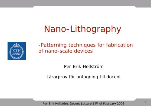
<strong>Nano</strong>-<strong>Lithography</strong><br />
-Patterning techniques for fabrication<br />
of nano-scale devices<br />
Per-Erik Hellström<br />
Lärarprov för antagning till docent<br />
Per-Erik Hellstöm, Docent Lecture 14 th of February 2006<br />
1
<strong>Nano</strong>-<strong>Lithography</strong><br />
Feature size < 100 nm<br />
Resist<br />
Per-Erik Hellstöm, Docent Lecture 14 th of February 2006<br />
2
• <strong>Nano</strong>-scale devices<br />
• Basics of optical lithography<br />
• Advanced optical lithography<br />
• <strong>Nano</strong>-lithography for low volume applications<br />
• Summary<br />
Per-Erik Hellstöm, Docent Lecture 14 th of February 2006<br />
3
<strong>Nano</strong>-Electronics<br />
poly-Si<br />
150nm<br />
50nm<br />
NiSi<br />
EKT at <strong>KTH</strong><br />
Per-Erik Hellstöm, Docent Lecture 14 th of February 2006<br />
4
<strong>Nano</strong>-wires in sensor application<br />
EKT at <strong>KTH</strong><br />
Si<br />
H=15 nm<br />
nanowire-FET<br />
W=15 nm<br />
Adsorption of<br />
DNA probes<br />
Capture of<br />
complementary DNA<br />
I<br />
I+ΔI 1<br />
I+ΔI 1 +ΔI 2<br />
Immobilization<br />
Hybridization<br />
Per-Erik Hellstöm, Docent Lecture 14 th of February 2006<br />
5
Photonic Crystals<br />
Ziyang Zhang, FMI at <strong>KTH</strong><br />
500 nm<br />
Per-Erik Hellstöm, Docent Lecture 14 th of February 2006<br />
6
<strong>Lithography</strong> specifications<br />
Resolution<br />
Pattern shape<br />
Large & small patterns<br />
Alignment<br />
Throughput<br />
Initial cost<br />
Running cost<br />
Ideal<br />
<strong>Lithography</strong><br />
Good<br />
Any<br />
Yes<br />
Good<br />
High<br />
Low<br />
Low<br />
Per-Erik Hellstöm, Docent Lecture 14 th of February 2006<br />
7
• <strong>Nano</strong>-scale devices<br />
• Basics of optical lithography<br />
– Projection lithography<br />
– Resolution<br />
• Advanced optical lithography<br />
• <strong>Nano</strong>-lithography for low volume applications<br />
• Summary<br />
Per-Erik Hellstöm, Docent Lecture 14 th of February 2006<br />
8
Projection <strong>Lithography</strong><br />
Intensity<br />
at mask<br />
Light source: λ<br />
Mask<br />
Intensity<br />
on wafer<br />
Light is diffracted<br />
Focusing lens<br />
Image on wafer<br />
Resist<br />
Per-Erik Hellstöm, Docent Lecture 14 th of February 2006<br />
9
Projection <strong>Lithography</strong><br />
Light source: λ<br />
Rayleigh criteria for<br />
resolving two point sources<br />
The resolution (R) is:<br />
Mask<br />
R<br />
λ<br />
= 0.61<br />
NA<br />
n<br />
α<br />
Numerical Aperture<br />
NA=n sin α<br />
Aerial image<br />
Resist<br />
Per-Erik Hellstöm, Docent Lecture 14 th of February 2006<br />
10
Projection <strong>Lithography</strong><br />
Light source: λ<br />
R<br />
=<br />
k<br />
1<br />
λ<br />
NA<br />
Mask<br />
Resolution factor k 1<br />
• mask design<br />
• resist process<br />
•k 1<br />
~0.6-0.8<br />
n<br />
α<br />
Numerical Aperture<br />
NA=n sin α<br />
Aerial image<br />
Resist<br />
I-line stepper in<br />
Electrum Laboratory<br />
λ=365 nm,NA=0.45,k 1<br />
=0.6<br />
⇒<br />
R≈500 nm<br />
Per-Erik Hellstöm, Docent Lecture 14 th of February 2006<br />
11
• <strong>Nano</strong>-scale devices<br />
• Basics of optical lithography<br />
• Advanced optical lithography<br />
– Shorter wavelength λ<br />
– Reduce resolution factor k 1<br />
– Increase lenses numerical aperture NA<br />
• <strong>Nano</strong>-lithography for low volume applications<br />
• Summary<br />
Per-Erik Hellstöm, Docent Lecture 14 th of February 2006<br />
12
Shorter wavelength<br />
R<br />
=<br />
k<br />
1<br />
λ<br />
NA<br />
λ [nm]<br />
436<br />
365<br />
248<br />
193<br />
Light source<br />
Hg arc lamp<br />
Hg arc lamp<br />
KrF excimer laser<br />
ArF excimer laser<br />
First year<br />
in production<br />
~1994<br />
~1997<br />
~2003<br />
157<br />
EUV 13.5<br />
F 2 excimer laser<br />
Laser or discharge of<br />
liquid target (Xe, Li…)<br />
CaF 2 lenses<br />
Reflective mirrors<br />
Per-Erik Hellstöm, Docent Lecture 14 th of February 2006<br />
13
Reduce resolution factor k 1<br />
Amplitude<br />
at Mask<br />
Normal Mask<br />
Phase Shift Mask<br />
R<br />
=<br />
d<br />
180° Phase Shift<br />
=<br />
k<br />
1<br />
λ<br />
NA<br />
λ<br />
2 −1<br />
( n )<br />
Amplitude<br />
at Wafer<br />
Intensity<br />
at Wafer<br />
• Different implementations on mask<br />
• Pattern dependent<br />
•k 1 can be reduced up to 40 %<br />
Per-Erik Hellstöm, Docent Lecture 14 th of February 2006<br />
14
Reduce resolution factor k 1<br />
Resist chemistry<br />
436, 365 nm: Photo-Active-Component (PAC)<br />
248,193 nm: Photo-Acid-Generator (PAG)<br />
R<br />
=<br />
k<br />
1<br />
λ<br />
NA<br />
Mask design and<br />
resist process<br />
Contrast<br />
436, 365 nm: γ=2-3, (Q f /Q 0 ≈2.5)<br />
248,193 nm: γ=5-10 (Q f /Q 0 ≈1.3)<br />
λ [nm]<br />
436<br />
365<br />
248<br />
193<br />
k 1<br />
0.8<br />
0.6<br />
0.3-0.4<br />
0.3-0.4<br />
Per-Erik Hellstöm, Docent Lecture 14 th of February 2006<br />
15
Increase NA<br />
R<br />
=<br />
k<br />
1<br />
λ<br />
NA<br />
Lens fabrication<br />
Immersion <strong>Lithography</strong><br />
λ [nm]<br />
436<br />
365<br />
248<br />
193<br />
NA<br />
0.15-0.45<br />
0.35-0.60<br />
0.35-0.82<br />
0.60-0.93<br />
n<br />
n H O<br />
α<br />
H 2<br />
O<br />
Numerical Aperture<br />
NA=n sin α<br />
= 1.44 ⇒ NA ≈1.36<br />
2<br />
Expected in production during 2006<br />
State of the Art: λ=193 nm, NA=0.93, k 1 =0.3 ⇒ R≈60 nm<br />
Per-Erik Hellstöm, Docent Lecture 14 th of February 2006<br />
16
Minimum feature size<br />
Production<br />
2003<br />
2005<br />
2007<br />
2009<br />
2011<br />
Technology<br />
Node<br />
90 nm<br />
65 nm<br />
45 nm<br />
32 nm<br />
22 nm<br />
Half pitch<br />
[nm]<br />
110<br />
105<br />
~80<br />
~ 55<br />
~39<br />
L G [nm]<br />
60<br />
42<br />
~30<br />
~21<br />
~16<br />
P. Bai, et. al., IEDM2005<br />
L G<br />
pitch<br />
λ=193nm<br />
λ=193nm<br />
immersion<br />
•193nm immersion<br />
with higher n?<br />
•EUV?<br />
Per-Erik Hellstöm, Docent Lecture 14 th of February 2006<br />
17
Why is optical lithography so<br />
succesful?<br />
•It’s not only resolution, it’s cost!<br />
193 nm lithography tool ~140 MSEK<br />
Mask set cost ~7 MSEK<br />
Affordable for high volume production<br />
due to high throughput ~100 wafer/hour<br />
Per-Erik Hellstöm, Docent Lecture 14 th of February 2006<br />
18
• <strong>Nano</strong>-scale devices<br />
• Basics of optical lithography<br />
• Advanced optical lithography<br />
• <strong>Nano</strong>-lithography for low volume applications<br />
– Electron Beam <strong>Lithography</strong><br />
– <strong>Nano</strong> Imprint <strong>Lithography</strong><br />
– Sidewall Transfer <strong>Lithography</strong><br />
• Summary<br />
Per-Erik Hellstöm, Docent Lecture 14 th of February 2006<br />
19
Electron beam lithography<br />
• Direct write<br />
• Arbitrary shape<br />
• λ < 0.1 nm<br />
• Beam width ~ 5 nm<br />
Per-Erik Hellstöm, Docent Lecture 14 th of February 2006<br />
20
Resolution of EB lithography<br />
• High Energy 100 keV<br />
• High contrast resist<br />
• Thin resist<br />
– Resist stack<br />
– Hard mask<br />
Thin resist<br />
Hard Mask<br />
Thick resist<br />
Wafer<br />
Wafer<br />
Per-Erik Hellstöm, Docent Lecture 14 th of February 2006<br />
21
Resolution of EB lithography<br />
• High Energy 100 keV<br />
• High contrast resist<br />
• Thin resist<br />
– Resist stack<br />
– Hard mask<br />
Resolution of equal lines and spaces<br />
Per-Erik Hellstöm, Docent Lecture 14 th of February 2006<br />
22
<strong>Nano</strong> Imprint <strong>Lithography</strong><br />
• Step and flash<br />
• Resolution ~10 nm<br />
• Arbitrary shape<br />
• Quartz master<br />
1X method<br />
• Alignment ~1 µm<br />
C.R.K. Marrian and D.M. Tennant, JVST, 2003<br />
50 nm pillars after 500 imprints<br />
with same master<br />
Per-Erik Hellstöm, Docent Lecture 14 th of February 2006<br />
23
Sidewall Transfer <strong>Lithography</strong><br />
• Combines lithography and process technology<br />
• In theory k 1 →0 for lines:<br />
R<br />
=<br />
k<br />
1<br />
λ<br />
NA<br />
• Pitch is determined by resolution of lithography<br />
• Optical lithography ⇒ high throughput<br />
Per-Erik Hellstöm, Docent Lecture 14 th of February 2006<br />
24
Sidewall Transfer <strong>Lithography</strong> Process<br />
Cross Section<br />
Top view<br />
Resist<br />
Si 0.2 Ge 0.8<br />
poly-Si<br />
SiO 2<br />
Wafer<br />
Per-Erik Hellstöm, Docent Lecture 14 th of February 2006<br />
25
Sidewall Transfer <strong>Lithography</strong> Process<br />
SiN<br />
Si 0.2 Ge 0.8<br />
poly-Si<br />
Cross Section<br />
Top view<br />
SiO 2<br />
Wafer<br />
Nitride<br />
100 nm<br />
Poly SiGe<br />
Oxide hard mask<br />
Per-Erik Hellstöm, Docent Lecture 14 th of February 2006<br />
26
Sidewall Transfer <strong>Lithography</strong> Process<br />
SiN<br />
Si 0.2 Ge 0.8<br />
poly-Si<br />
SiO 2<br />
Wafer<br />
Cross Section<br />
Top view<br />
Per-Erik Hellstöm, Docent Lecture 14 th of February 2006<br />
27
Sidewall Transfer <strong>Lithography</strong> Process<br />
SiN<br />
Resist<br />
poly-Si<br />
SiO 2<br />
Wafer<br />
Cross Section<br />
Top view<br />
Per-Erik Hellstöm, Docent Lecture 14 th of February 2006<br />
28
Sidewall Transfer <strong>Lithography</strong> Process<br />
SiN<br />
Resist<br />
poly-Si<br />
SiO 2<br />
Wafer<br />
Cross Section<br />
Top view<br />
Per-Erik Hellstöm, Docent Lecture 14 th of February 2006<br />
29
Sidewall Transfer <strong>Lithography</strong> Process<br />
SiN<br />
Resist<br />
poly-Si<br />
SiO 2<br />
Wafer<br />
Cross Section<br />
Top view<br />
Per-Erik Hellstöm, Docent Lecture 14 th of February 2006<br />
30
Sidewall Transfer <strong>Lithography</strong> Process<br />
SiN<br />
Cross Section<br />
Top view<br />
poly-Si<br />
SiO 2<br />
Wafer<br />
Per-Erik Hellstöm, Docent Lecture 14 th of February 2006<br />
31
Sidewall Transfer <strong>Lithography</strong><br />
10 poly-Si lines<br />
Width=45 nm<br />
poly-Si<br />
50nm<br />
150nm<br />
NiSi<br />
poly-Si contact<br />
Si<br />
H=15 nm<br />
W=15 nm<br />
Per-Erik Hellstöm, Docent Lecture 14 th of February 2006<br />
32
Sidewall Transfer <strong>Lithography</strong><br />
Line Width Roughness is small for STL<br />
Resist<br />
Roughness along a resist edge<br />
is called Line Edge Roughness<br />
Per-Erik Hellstöm, Docent Lecture 14 th of February 2006<br />
33
Sidewall Transfer <strong>Lithography</strong><br />
Line Width Roughness is small for STL<br />
STL<br />
STL EB ArF<br />
A. Kaneko, et. al., IEDM2005<br />
Per-Erik Hellstöm, Docent Lecture 14 th of February 2006<br />
34
Summary<br />
Ideal<br />
Advanced<br />
Optical<br />
Electron<br />
Beam<br />
<strong>Nano</strong><br />
Imprint<br />
Sidewall<br />
Transfer<br />
Resolution<br />
Good<br />
Good<br />
Good<br />
Good<br />
Good<br />
Pattern shape<br />
Any<br />
Any<br />
Any<br />
Any<br />
Lines/<br />
Rings<br />
Large & small<br />
patterns<br />
Yes<br />
Yes<br />
No<br />
Yes<br />
Yes<br />
Alignment<br />
Good<br />
Good<br />
Good<br />
Poor<br />
Good<br />
Throughput<br />
High<br />
High<br />
Low<br />
Medium<br />
High<br />
Initial cost<br />
Low<br />
High<br />
Medium<br />
Low<br />
Low<br />
Running cost<br />
Low<br />
High<br />
Low<br />
Medium<br />
Low<br />
Per-Erik Hellstöm, Docent Lecture 14 th of February 2006<br />
35