A Full-Bridge DC-DC Converter with Zero- Voltage Switching ... - ijcee
A Full-Bridge DC-DC Converter with Zero- Voltage Switching ... - ijcee
A Full-Bridge DC-DC Converter with Zero- Voltage Switching ... - ijcee

Create successful ePaper yourself
Turn your PDF publications into a flip-book with our unique Google optimized e-Paper software.
International Journal of Computer and Electrical Engineering, Vol. 3, No. 2, April, 2011<br />
1793-8163<br />
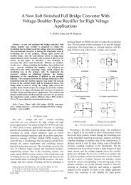
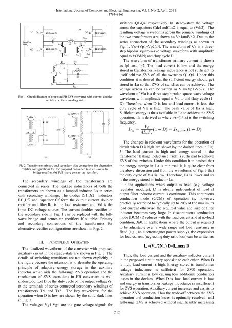
Fig. 1. Circuit diagram of proposed FB ZVS converter <strong>with</strong> current doubler<br />
rectifier on the secondary side.<br />
switches Q1-Q4, respectively. In steady-state the voltage<br />
across the capacitors Cdc1andCdc2 is equal to (Vd/2) . The<br />
resulting voltage waveforms across the primary windings of<br />
the two transformers are shown as Vp1andVp2 .Due to the<br />
series connection of the secondary windings as shown in<br />
Fig. 1, Vs=(Vp1+Vp2)/N. The waveform of Vs is a threestep<br />
bipolar square-wave voltage waveform <strong>with</strong> amplitude<br />
equal to ±(Vd/N) and duty cycle D.<br />
The waveform of transformer primary current is shown<br />
as Ip1 and Ip2. The load current is low and the energy<br />
stored in transformer leakage inductance is not sufficient to<br />
itself achieve ZVS of all the switches Q1-Q4. Under this<br />
condition it is desired that the sufficient energy should get<br />
stored in La so that ZVS of switches can be achieved. The<br />
voltage across La can be written as Vla=(Vp1-Vp2) . The<br />
waveform of Vla is a three-step bipolar square-wave voltage<br />
waveform <strong>with</strong> amplitude equal ± Vd to and duty cycle (1-<br />
D). Therefore, when D is low and load current is less, the<br />
duty cycle of Vla is high. The peak value of Ila is high.<br />
Sufficient energy is thus available in La to achieve the ZVS<br />
operation. Ila is derived as where Fs=(1/Ts) is the switching<br />
frequency.<br />
Fig 2. Transformer primary and secondary side connections for alternative<br />
rectifier configurations for the proposed converter. (a) <strong>Full</strong> –wave full<br />
bridge rectifier. (b) <strong>Full</strong> -wave center- tap rectifier.<br />
The secondary windings of the transformers are<br />
connected in series. The leakage inductances of both the<br />
transformers are shown as a lumped inductor Ls in series<br />
<strong>with</strong> secondary windings. The diodes Dr1,Dr2 inductors<br />
Lf1,Lf2 and capacitor Cf form the output current doubler<br />
rectifier and filter.Ro is the load resistance and Vd is the<br />
input <strong>DC</strong> voltage source. The current doubler rectifier on<br />
the secondary side in Fig. 1 can be replaced <strong>with</strong> the fullwave<br />
bridge and center-tap rectifiers if suitable. Primary<br />
and secondary connections of the transformers for<br />
alternative rectifier configurations are shown in Fig. 2.<br />
III. PRINCIPLE OF OPERATION<br />
The idealized waveforms of the converter <strong>with</strong> proposed<br />
auxiliary circuit in the steady-state are shown in Fig. 3. The<br />
details of switching transitions are not shown explicitly in<br />
the figure because the intension is to describe the operating<br />
principle of adaptive energy storage in the auxiliary<br />
inductor which aids the full-range ZVS operation and the<br />
mechanism of ZVS transitions in FB converters is well<br />
understood. Let D be the duty cycle of the output voltageVs ,<br />
at the terminals of series-connected secondary windings of<br />
transformers Tr1 and Tr2. The key waveforms for the<br />
operation when D is low are shown by the solid dark lines<br />
in Fig. 3.<br />
The voltages Vg1-Vg4 are the gate voltage signals for<br />
The changes in relevant waveforms for the operation of<br />
circuit when D is high are shown by the dashed lines in Fig.<br />
3. The load current is high and energy stored in the<br />
transformer leakage inductance itself is sufficient to achieve<br />
ZVS of the switches. Under this condition it is desired that<br />
the energy storage in La is minimal. It is quite clear from<br />
the above discussion and from the waveforms of Fig. 3 that<br />
the duty cycle of Vla is low. Therefore, Ila is lower and so<br />
is the energy stored in inductor La.<br />
In the applications where output is fixed (e.g. voltage<br />
regulator modules), D is ideally independent of load if<br />
output filter inductor current is continuous. This continuous<br />
conduction mode (CCM) of operation is, however,<br />
practically restricted to typically up to 20% of the maximum<br />
load current otherwise the required value and size of filter<br />
inductor becomes very large. In discontinuous conduction<br />
mode (<strong>DC</strong>M) D reduces <strong>with</strong> the load current and at no-load<br />
condition,D≅0. In applications where the output is required<br />
to be adjustable over a wide range and load resistance is<br />
fixed (e.g., an electromagnet power supply), the expression<br />
for load current (neglecting duty ratio loss) can be written as<br />
I o =(V d /2N ro ) D=I o ,max D<br />
Thus, the load current and the auxiliary inductor current<br />
in the proposed circuit vary opposite to each other. When D<br />
is high, load current is high. Energy stored in transformer<br />
leakage inductance is sufficient for ZVS operation.<br />
Auxiliary current is low causing low additional conduction<br />
losses in the devices. When D is low, load current is low<br />
and energy in transformer leakage inductance is insufficient<br />
for ZVS operation. Auxiliary current increases and assists to<br />
achieve ZVS operation. Thus the trade-off between the ZVS<br />
operation and conduction losses is optimally resolved and<br />
full-range ZVS is achieved <strong>with</strong>out significantly increasing<br />
212