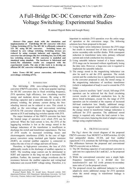
A Full-Bridge DC-DC Converter with Zero- Voltage Switching ... - ijcee
A Full-Bridge DC-DC Converter with Zero- Voltage Switching ... - ijcee
A Full-Bridge DC-DC Converter with Zero- Voltage Switching ... - ijcee

You also want an ePaper? Increase the reach of your titles
YUMPU automatically turns print PDFs into web optimized ePapers that Google loves.
International Journal of Computer and Electrical Engineering, Vol. 3, No. 2, April, 2011<br />
1793-8163<br />
A <strong>Full</strong>-<strong>Bridge</strong> <strong>DC</strong>-<strong>DC</strong> <strong>Converter</strong> <strong>with</strong> <strong>Zero</strong>-<br />
<strong>Voltage</strong> <strong>Switching</strong>: Experimental Studies<br />
R.samuel Rajesh Babu and Joseph Henry<br />
Abstract—This paper deals <strong>with</strong> the simulation and<br />
implementation of <strong>Full</strong>-<strong>Bridge</strong> <strong>DC</strong>-<strong>DC</strong> converter <strong>with</strong> <strong>Zero</strong><br />
<strong>Voltage</strong> <strong>Switching</strong> (ZVS). The 48V <strong>DC</strong> is efficiently reduced to<br />
12V <strong>DC</strong> using <strong>DC</strong>-<strong>DC</strong> converter. <strong>Switching</strong> losses are<br />
reduced by zero voltage switching. <strong>Switching</strong> stresses are<br />
reduced by using resonant inductor and capacitor. This<br />
converter has advantages like low switching loss, less EMI, and<br />
less switching stresses. <strong>DC</strong>-<strong>DC</strong> converter is modelled and<br />
simulated using simulink. The hardware is fabricated and<br />
tested..The simulation results are compared <strong>with</strong> the<br />
experimental results. The aim of this work is to develop an<br />
efficient <strong>DC</strong>-<strong>DC</strong> converter <strong>with</strong> high power density.<br />
Index Terms—<strong>DC</strong>-<strong>DC</strong> power conversion, soft-switching,<br />
zerovoltage- switching (ZVS).<br />
I. INTRODUCTION<br />
The full-bridge (FB) zero-voltage-switching (ZVS)<br />
converter (FBZVS converter), is the most popular topology<br />
for <strong>DC</strong>-<strong>DC</strong> converters due to fixed switching frequency,<br />
ZVS operation, high efficiency, low circulating reactive<br />
energy and moderate device stresses. By using a <strong>DC</strong><br />
blocking capacitor and a saturable inductor in series <strong>with</strong><br />
primary winding, the primary current during the freewheeling<br />
interval can be reduced to zero. This circuit is<br />
called as the zero-voltage and zero-current switching<br />
(ZVZCS) FB converter wherein the lagging-leg switches<br />
operate at ZCS and leading-leg switches operate <strong>with</strong> ZVS.<br />
The major limitation of the FBZVS converter has been<br />
the limited range of operation over which ZVS can be<br />
achieved. When the load current is low, the ZVS of the<br />
lagging-leg switches is lost as the energy stored in the<br />
leakage inductance of the transformer is insufficient to<br />
discharge the switch and transformer capacitances. The loss<br />
of ZVS results in increased switching losses and<br />
electromagnetic interference (EMI). In the case of highpower<br />
converters using insulated gate bipolar transistor<br />
(IGBT), an external snubber capacitor is connected to<br />
reduce the rate of rise of voltage and turn-off losses.<br />
Therefore, in high-power converters, the loss of ZVS<br />
additionally results in the discharge of snubber capacitor in<br />
IGBT. The resulting surge current can be detrimental to<br />
IGBT and capacitor in the long run and it increases EMI<br />
problem. Further, the resonant voltage overshoots due to<br />
resonance between the snubber capacitor and wiring/lead<br />
inductance can exceed IGBT voltage rating. Therefore, it is<br />
Manuscript received June 10, 2010.<br />
R.samuel Rajesh Babu, Dr. Joseph henry, Research scholar, EEE<br />
department,Professor, EEE Department. Sathyabama University, Vel Tech<br />
University, Chennai, India.(e-mail: Samuel.rajeshbabu@gmail.com)<br />
important to maintain ZVS operation over the entire range<br />
of operation or the conversion range. The following<br />
solutions have been proposed in the past.<br />
1) Using higher series inductance increases the ZVS range<br />
but results in increased loss of duty cycle and ringing<br />
across secondary-side rectifier diodes. With consequent<br />
reduction in transformer turns ratio, primary reflected<br />
current and switch conduction loss increases.<br />
2) Using saturable inductor instead of a linear inductor,<br />
ZVS range can be increased <strong>with</strong>out significantly losing<br />
the duty ratio. However, a large-size core is required to<br />
implement the saturable inductor.<br />
3) The energy stored in the magnetizing inductance can<br />
also be used to aid the ZVS operation. The switch<br />
current and the conduction loss is significantly increased.<br />
In the converter proposed in and, the stored energy in<br />
the magnetizing inductance of auxiliary transformer<br />
(which is independent of load) is used to extend the ZVS<br />
range.<br />
4) Using a passive auxiliary “pole” circuit, full-range ZVS<br />
operation can be achieved but the fixed circulating<br />
current results in additional conduction loss. In the<br />
above listed techniques, except for, the range of ZVS<br />
operation can be extended at the expense of increased<br />
full-load conduction loss. Ideally, additional energy<br />
storage is not required under full-load condition since<br />
the energy stored in transformer leakage inductance is<br />
sufficient for ZVS operation. The additional stored<br />
energy is required only when the load current is less.<br />
FBZVS converters featuring this kind of adaptive energy<br />
storage using coupled inductors.<br />
II. FB ZVS CONVERTER<br />
The Fig.1 shows the circuit diagram of the proposed<br />
FBZVS converter. Four MOSFET or IGBTswitches, Q1-Q4,<br />
four antiparallel diodes, D1-D4, and four snubber<br />
capacitorsC1-C4, constitute the full-bridge switching circuit.<br />
The differences between the proposed and conventional<br />
FBZVS converter are as follows.<br />
1) The <strong>DC</strong> blocking capacitor of conventional converter is<br />
split into two capacitors,Cdc1 andCdc2 , in the proposed<br />
circuit.<br />
2) While the conventional converter uses a single highfrequency<br />
transformer, it is divided into two<br />
transformersTr1 and Tr2 (<strong>with</strong> primary-to-secondary<br />
turns ratio of ) in the proposed circuit.<br />
3) The proposed circuit has additional inductor La which<br />
adaptively stores additional energy for ZVS operation<br />
when the stored energy in transformer leakage is<br />
inadequate.<br />
211
International Journal of Computer and Electrical Engineering, Vol. 3, No. 2, April, 2011<br />
1793-8163<br />
Fig. 1. Circuit diagram of proposed FB ZVS converter <strong>with</strong> current doubler<br />
rectifier on the secondary side.<br />
switches Q1-Q4, respectively. In steady-state the voltage<br />
across the capacitors Cdc1andCdc2 is equal to (Vd/2) . The<br />
resulting voltage waveforms across the primary windings of<br />
the two transformers are shown as Vp1andVp2 .Due to the<br />
series connection of the secondary windings as shown in<br />
Fig. 1, Vs=(Vp1+Vp2)/N. The waveform of Vs is a threestep<br />
bipolar square-wave voltage waveform <strong>with</strong> amplitude<br />
equal to ±(Vd/N) and duty cycle D.<br />
The waveform of transformer primary current is shown<br />
as Ip1 and Ip2. The load current is low and the energy<br />
stored in transformer leakage inductance is not sufficient to<br />
itself achieve ZVS of all the switches Q1-Q4. Under this<br />
condition it is desired that the sufficient energy should get<br />
stored in La so that ZVS of switches can be achieved. The<br />
voltage across La can be written as Vla=(Vp1-Vp2) . The<br />
waveform of Vla is a three-step bipolar square-wave voltage<br />
waveform <strong>with</strong> amplitude equal ± Vd to and duty cycle (1-<br />
D). Therefore, when D is low and load current is less, the<br />
duty cycle of Vla is high. The peak value of Ila is high.<br />
Sufficient energy is thus available in La to achieve the ZVS<br />
operation. Ila is derived as where Fs=(1/Ts) is the switching<br />
frequency.<br />
Fig 2. Transformer primary and secondary side connections for alternative<br />
rectifier configurations for the proposed converter. (a) <strong>Full</strong> –wave full<br />
bridge rectifier. (b) <strong>Full</strong> -wave center- tap rectifier.<br />
The secondary windings of the transformers are<br />
connected in series. The leakage inductances of both the<br />
transformers are shown as a lumped inductor Ls in series<br />
<strong>with</strong> secondary windings. The diodes Dr1,Dr2 inductors<br />
Lf1,Lf2 and capacitor Cf form the output current doubler<br />
rectifier and filter.Ro is the load resistance and Vd is the<br />
input <strong>DC</strong> voltage source. The current doubler rectifier on<br />
the secondary side in Fig. 1 can be replaced <strong>with</strong> the fullwave<br />
bridge and center-tap rectifiers if suitable. Primary<br />
and secondary connections of the transformers for<br />
alternative rectifier configurations are shown in Fig. 2.<br />
III. PRINCIPLE OF OPERATION<br />
The idealized waveforms of the converter <strong>with</strong> proposed<br />
auxiliary circuit in the steady-state are shown in Fig. 3. The<br />
details of switching transitions are not shown explicitly in<br />
the figure because the intension is to describe the operating<br />
principle of adaptive energy storage in the auxiliary<br />
inductor which aids the full-range ZVS operation and the<br />
mechanism of ZVS transitions in FB converters is well<br />
understood. Let D be the duty cycle of the output voltageVs ,<br />
at the terminals of series-connected secondary windings of<br />
transformers Tr1 and Tr2. The key waveforms for the<br />
operation when D is low are shown by the solid dark lines<br />
in Fig. 3.<br />
The voltages Vg1-Vg4 are the gate voltage signals for<br />
The changes in relevant waveforms for the operation of<br />
circuit when D is high are shown by the dashed lines in Fig.<br />
3. The load current is high and energy stored in the<br />
transformer leakage inductance itself is sufficient to achieve<br />
ZVS of the switches. Under this condition it is desired that<br />
the energy storage in La is minimal. It is quite clear from<br />
the above discussion and from the waveforms of Fig. 3 that<br />
the duty cycle of Vla is low. Therefore, Ila is lower and so<br />
is the energy stored in inductor La.<br />
In the applications where output is fixed (e.g. voltage<br />
regulator modules), D is ideally independent of load if<br />
output filter inductor current is continuous. This continuous<br />
conduction mode (CCM) of operation is, however,<br />
practically restricted to typically up to 20% of the maximum<br />
load current otherwise the required value and size of filter<br />
inductor becomes very large. In discontinuous conduction<br />
mode (<strong>DC</strong>M) D reduces <strong>with</strong> the load current and at no-load<br />
condition,D≅0. In applications where the output is required<br />
to be adjustable over a wide range and load resistance is<br />
fixed (e.g., an electromagnet power supply), the expression<br />
for load current (neglecting duty ratio loss) can be written as<br />
I o =(V d /2N ro ) D=I o ,max D<br />
Thus, the load current and the auxiliary inductor current<br />
in the proposed circuit vary opposite to each other. When D<br />
is high, load current is high. Energy stored in transformer<br />
leakage inductance is sufficient for ZVS operation.<br />
Auxiliary current is low causing low additional conduction<br />
losses in the devices. When D is low, load current is low<br />
and energy in transformer leakage inductance is insufficient<br />
for ZVS operation. Auxiliary current increases and assists to<br />
achieve ZVS operation. Thus the trade-off between the ZVS<br />
operation and conduction losses is optimally resolved and<br />
full-range ZVS is achieved <strong>with</strong>out significantly increasing<br />
212
International Journal of Computer and Electrical Engineering, Vol. 3, No. 2, April, 2011<br />
1793-8163<br />
full-load conduction losses . Although the proposed<br />
FBZVS converter has two transformers, the combined<br />
ratings of the two transformers is the same as one<br />
transformer in the conventional FBZVS converter.<br />
the rectifier. For this case the fundamental component of the<br />
square wave voltage is used in the ac analysis.<br />
48v <strong>DC</strong> is converted into high frequency AC using as<br />
inverter. This is stepped down to 12v by using a step down<br />
transformer. Further this is rectified and filtered using LC<br />
filter. <strong>Switching</strong> losses are reduced by zero voltage<br />
switching. <strong>Switching</strong> stresses are reduced by using resonant<br />
inductor and capacitor The even harmonics in the output of<br />
the rectifier are filtered using LC filter. Driving pulses are<br />
applied to the IGBT’S in such a way that the pulse width<br />
coincides <strong>with</strong> the resonant period.<br />
The primary voltage of the high frequency transformer as<br />
shown in (1),<br />
(1)<br />
The magnetizing current i M (t) is<br />
As for the primary winding, the dot end of the secondary<br />
winding is more positive that the non-dot ends. This implies<br />
that diode D1 & D2 is conducting while D3 & D4 is not<br />
conducting. The secondary voltage can be computed as in<br />
(3).<br />
(2)<br />
Fig .3. Idealized steady-state waveforms of proposed converter<br />
The primary voltage of the individual transformer in<br />
proposed converter (±Vd/2, peak) is half as compared to<br />
that in conventional converter (±Vd , peak) Thus the total<br />
volt-ampere rating of two transformer in proposed converter<br />
is the same as single transformer in conventional converter.<br />
In high-power applications two half-rated transformers in<br />
proposed converter can ease thermal management. Similarly,<br />
the worst-case <strong>DC</strong> voltage(±Vd) that might appear across<br />
two <strong>DC</strong> blocking capacitors in the proposed converter is the<br />
same as that in the conventional FBZVS converter.<br />
IV.<br />
ANALYSIS AND DESIGN OF FULL BRIDGE <strong>DC</strong>-<strong>DC</strong><br />
CONVERTER<br />
The <strong>Full</strong>-<strong>Bridge</strong> <strong>DC</strong>-<strong>DC</strong> converter applies a square wave<br />
of voltage to a resonant network. The resonant network has<br />
the effect of filtering the higher harmonic voltages so that,<br />
essentially, a sine wave of current appears at the input to the<br />
resonant circuit (this is true over most of the load range of<br />
interest). This fact allows classical ac analysis techniques to<br />
be used.<br />
The fundamental component of the square wave input<br />
voltage is applied to the resonant network, and the resulting<br />
sine waves of current and voltage in the resonant circuit are<br />
computed using classical AC analysis. For a rectifier <strong>with</strong><br />
an inductor output filter, the sine wave voltage at the input<br />
to the rectifier is rectified, and the average value takes to<br />
arrive at the resulting dc output voltage. For a capacitive<br />
output filter, a square wave of voltage appears at the input<br />
to the rectifier while a sine wave of current is injected into<br />
The current flowing into the inductor was calculated by<br />
using (4),<br />
The output voltage across the inductor Lo as shown in<br />
(5),<br />
The output voltage is shown in (6),<br />
The primary voltage of the high frequency transformer as<br />
shown in (7),<br />
The magnetizing current of the high frequency<br />
transformer is as shown in (8),<br />
(3)<br />
(4)<br />
(5)<br />
(6)<br />
(7)<br />
213
International Journal of Computer and Electrical Engineering, Vol. 3, No. 2, April, 2011<br />
1793-8163<br />
In this instance, as at the primary, the dot ends are more<br />
negative than the non-dot ends, which results in (9).<br />
The output voltage across the inductor is shown in (10).<br />
(8)<br />
(9)<br />
(10)<br />
The output current flowing through the inductor is<br />
shown in (11).<br />
(11)<br />
Output power is shown in Fig 5h. It can be seen that the<br />
output is free from ripple.The specifications are as follows:<br />
DESIGN PARAMETER<br />
Input <strong>Voltage</strong><br />
L<br />
C 1 =C 2<br />
L f<br />
C f<br />
R<br />
T ON 50 %<br />
T OFF 50 %<br />
T 100 %<br />
Duty Cycle 50 %<br />
<strong>Switching</strong> Frequency 50 KHz<br />
Transformer Ratio 4:1<br />
Output <strong>Voltage</strong><br />
12V<br />
Output Current<br />
4 A<br />
POWER<br />
48 W<br />
DIODE<br />
IN4007<br />
MOSFET<br />
IRF840<br />
RATING<br />
48V<br />
100 micro H<br />
100 micro F<br />
0.01 pico H<br />
2200 micro F<br />
3 Ω<br />
The output voltage across the capacitor Co was<br />
calculated using (12),<br />
(12)<br />
The output voltage can be obtained across the load is<br />
shown in (13),<br />
(13)<br />
The output power of the converter is shown in (14),<br />
(14)<br />
Fig 5a. Circuit diagram<br />
The average input current can be calculated by using<br />
(15)<br />
where I in,av , is the average input current and δ= 0.8.<br />
The efficiency of the converter is shown in (16),<br />
(16)<br />
Fig 5b. Input voltage<br />
V. SIMULATION RESULTS<br />
ZVS <strong>DC</strong>-<strong>DC</strong> converter is modelled using the blocks of<br />
Simulink and the results are presented in this section.The<br />
circuit of ZVS <strong>DC</strong>-<strong>DC</strong> converter is shown in fig 5a.Input<br />
voltage is shown in Fig 5b.Driving pulse and voltage across<br />
Q3 switch are shown in Fig 5c. Inverter output voltage is<br />
shown in Fig 5d. Transformer winding –1 is voltage shown<br />
in Fig 5e . Transformer winding –2 is voltage shown in Fig<br />
5f .<strong>DC</strong> output voltage and current are shown in Fig 5g..<br />
214<br />
Fig 5c. Driving pulse and voltage across Q3 switch
International Journal of Computer and Electrical Engineering, Vol. 3, No. 2, April, 2011<br />
1793-8163<br />
Fig 5d .Inverter output voltage<br />
FB ZVS converter is proposed to achieve ZVS over entire<br />
conversion range <strong>with</strong> minimum additional conduction loss.<br />
The proposed converter does not use auxiliary coupled<br />
inductor or transformer, rather, the main power transformer<br />
is divided into two half-rated transformers and an uncoupled<br />
inductor is used to achieve ZVS over entire conversion<br />
range. The proposed converter has following advantages<br />
like low switching loss ,less EMI, less switching stresses<br />
and high efficiency. It is particularly suitable in applications<br />
where the output is required to be adjustable over a wide<br />
range and load resistance is fixed (e.g. an electromagnet<br />
power supply).<br />
A. Input <strong>Voltage</strong> vs Output Power<br />
Fig 5e Transformer winding –1 voltage<br />
Fig 5f .Transformer winding –2 voltage<br />
INPUT<br />
VOLTAGE<br />
OUTPUT<br />
POWER(CONVENTIONAL<br />
CONVERTER)<br />
OUTPUT<br />
POWER(PROPOSED<br />
CONVERTER)<br />
220 915 1089<br />
250 1186 1413<br />
280 1492 1775<br />
B. Input Power vs Output Power<br />
Fig 5g. Output voltage and current<br />
Fig 5h. Output power<br />
VI.<br />
COMPARISON OF CONVENTIONAL AND PRPPOSED FULL<br />
BRIDGE <strong>DC</strong>-<strong>DC</strong> CONVERTER<br />
The conventional FB ZVS converter uses a transformer<br />
and an uncoupled inductor to achieve ZVS operation over<br />
the entire conversion range . In this paper a new topology of<br />
INPUT<br />
POWER<br />
OUTPUT<br />
POWER(CONVENTIONAL<br />
CONVERTER)<br />
OUTPUT<br />
POWER(PROPOSED<br />
CONVERTER)<br />
2008 915 1089<br />
2108 1186 1413<br />
2378 1492 1775<br />
215
C. Input <strong>Voltage</strong> vs Efficiency<br />
International Journal of Computer and Electrical Engineering, Vol. 3, No. 2, April, 2011<br />
1793-8163<br />
Fig 7a.Hardware layout of FB ZVS converter<br />
INPUT<br />
VOLTAGE<br />
EFFICIENCY OF<br />
CONVENTIONAL<br />
CONVERTER<br />
EFFICIENCY OF<br />
PROPOSED<br />
CONVERTER<br />
44 71 79<br />
48 74 81<br />
52 76 83<br />
56 77 84<br />
VII. EXPERIMENTAL RESULTS<br />
The hardware for <strong>DC</strong>-<strong>DC</strong> converter is fabricated in the<br />
laboratory <strong>with</strong> resistive load. Pulses required by the IGBT’<br />
s are generated by using a microcontroller. These pulses are<br />
amplified by using a driver amplifier. The hardware<br />
implementation details are shown in Fig. 7a. The hardware<br />
consists of power circuit and microcontroller based control<br />
circuit. The pulses are generated by using the ATMEL<br />
microcontroller 89C2051.<br />
These pulses are amplified using the driver IC IR2110.<br />
Control circuit for generating the driving pulses is shown in<br />
Fig. 7b. The AC input voltage is shown in Fig. 7c. The<br />
pulses generated by the microcontroller are shown in Fig.<br />
7d. The inverter output voltage is shown in Fig. 7e. The<br />
transformer primary side voltage is shown in Fig. 7f. The<br />
transformer secondary side voltage is shown in Fig. 7g.<br />
The <strong>DC</strong> output voltage is shown in Fig. 7h. The<br />
specifications are as follows:<br />
DESIGN PARAMETER<br />
RATING<br />
Input <strong>Voltage</strong><br />
48V<br />
L<br />
26 milli H<br />
C 1 =C 2<br />
2200 micro F,63 V,83 C<br />
L f<br />
7 milli H<br />
C f<br />
47 micro F,63 V,83 C<br />
R<br />
3 Ω<br />
Transformer<br />
500 milli Amp<br />
MOSFET<br />
IRF840<br />
DIODE<br />
IN5408<br />
Duty Cycle 50 %<br />
<strong>Switching</strong> Frequency 50 KHz<br />
Transformer Ratio 4:1<br />
Output <strong>Voltage</strong><br />
12V<br />
Output Current<br />
4 A<br />
Power<br />
48 W<br />
Fig.7b Control circuit for generating the driving pulses<br />
Fig 7c. AC Input <strong>Voltage</strong><br />
Fig 7d. Driving Pulses<br />
216
International Journal of Computer and Electrical Engineering, Vol. 3, No. 2, April, 2011<br />
1793-8163<br />
Fig. 7e. Inverter Output <strong>Voltage</strong><br />
VIII. CONCLUSION:<br />
A <strong>Full</strong>-<strong>Bridge</strong> <strong>DC</strong>-<strong>DC</strong> converter <strong>with</strong> <strong>Zero</strong> <strong>Voltage</strong><br />
<strong>Switching</strong> (ZVS) is modelled using the blocks of simulink.<br />
Input <strong>DC</strong> is converted to high frequency AC and it is<br />
stepped down to 12V level. Latter it is rectified using full<br />
wave rectifier. Soft switched <strong>DC</strong>-<strong>DC</strong> <strong>Converter</strong> is analysed ,<br />
simulated and results are presented. <strong>Switching</strong> losses are<br />
reduced by zero voltage switching. <strong>Switching</strong> stresses are<br />
reduced by using resonant inductor and capacitor. This<br />
converter has advantages like higher output current, smaller<br />
transformer and reduced filter size. The efficiency is<br />
improved by using soft switching. Power density is<br />
increased by reducing the volume. The volume is reduced<br />
due to the increased frequency. This converter can be used<br />
for battery charging, control of <strong>DC</strong> drives Electrolysis and<br />
high power applications. ZVS full bridge <strong>DC</strong> to <strong>DC</strong><br />
converter is simulated and implemented. From the<br />
simulation and experimental results,it can be seen that the<br />
experimental results are similar to simulation results.<br />
Fig 7f. Transformer primary side voltage<br />
Fig 7g. Transformer secondary side voltage<br />
Fig. 7h .<strong>DC</strong> Output <strong>Voltage</strong><br />
REFERENCES<br />
[1] R. A. Fischer, R. D. T. Ngo, and M. H. Kuo, “A 500 kHz, 250W dc–<br />
dcconverter <strong>with</strong> multiple outputs controlled by phase-shifted PWM<br />
and magnetic,” in Proc. High Freq Power Conv., May 1988, pp. 100–<br />
110.<br />
[2] J. A. Sabate, V. Vlatkovic, R. B. Ridley, F. C. Lee, and B. H.<br />
Cho,“Design considerations for high-voltage high-power full-bridge<br />
zerovoltage- switching PWM converter,” in Proc. IEEE Appl. Power<br />
Electron.Conf. (APEC), 1990, pp. 275–284.<br />
[3] D. Dalal, “A 500 kHz multi-output converter <strong>with</strong> zero voltage<br />
switching,” in Proc. IEEE Appl. Power Electron. Conf. (APEC), 1990,<br />
pp. 265–274.<br />
[4] F.-S. Tsai, “Small-signal and transient analysis of a zerovoltageswitched,phase<br />
controlled PWM converter using averaged<br />
switch model,” IEEE Trans. Ind. Appl., vol. 29, no. 3, pp. 493–499,<br />
May/Jun.1993.<br />
[5] A. W. Lotfi, Q. Chen, and F. C. Lee, “Non-linear optimization tool<br />
for the full-bridge zero-voltage-switched dc–dc convertor,” Proc.<br />
Inst.Elect. Eng. B, vol. 140, no. 5, pp. 289–296, Sep. 1993.<br />
[6] J. G. Cho, J. A. Sabate, G. Hua, and F. C. Lee, “<strong>Zero</strong>-voltage and<br />
zero-current-switching full bridge PWM converter for high power<br />
applications,”IEEE Trans. Power Electron., vol. 11, no. 4, pp. 622–<br />
627, Jul. 1996.<br />
[7] G. Hua, F. C. Lee, and M. M. Jovanovic, “An improved full-bridge<br />
zero-voltage-switched PWM converter using a saturable inductor,”<br />
IEEE Trans. Power Electron., vol. 8, no. 4, pp. 530–534, Oct. 1993.<br />
[8] S. Hamada and M. Nakaoka, “Analysis and design of a saturable<br />
reactor assisted soft-switching full-bridge dc–dc converter,” IEEE<br />
Trans.Power Electron., vol. 9, no. 3, pp. 309–317, May 1994.<br />
[9] [R.Watson and F. C. Lee, “Analysis, design and experimental results<br />
of a 1-kW FB-ZVS-PWM converter employing magamp secondary<br />
side control,” IEEE Trans. Ind. Electron., vol. 45, no. 5, pp. 806–814,<br />
Oct. 1998.<br />
[10] R. Ayyanar and N. Mohan, “Novel soft-switched dc–dc converter<br />
<strong>with</strong> full ZVS-range and reduced filter requirement—Part I:<br />
Regulated-output applications,” IEEE Trans. Power. Electron., vol.<br />
16, no.2, pp. 184–192, Mar. 2001.<br />
[11] R. Ayyanar and N. Mohan, “Novel soft-switched dc–dc converter<br />
<strong>with</strong> full ZVS-range and reduced filter requirement Part II: Constantinput,<br />
variable-output applications,” IEEE Trans. Power. Electron.,<br />
vol. 16, no. 2, pp. 193–200, Mar. 2001.<br />
[12] P. K. Jain, W. Kang, H. Soin, and Y. Xi, “Analysis and design<br />
considerations of a load and line independent zero voltage switching<br />
full bridge <strong>DC</strong>/<strong>DC</strong> converter topology,” IEEE Trans. Power Electron.,<br />
vol. 17, no. 5, pp. 649–657, Sep. 2002.<br />
[13] Y. Jang, M. M. Jovanovic, and Y. Chang, “A new ZVS-PWM<br />
fullbridge converter,” IEEE Trans. Power Electron., vol. 18, no. 5,<br />
pp.1122–1129, Sep. 2003.<br />
217
International Journal of Computer and Electrical Engineering, Vol. 3, No. 2, April, 2011<br />
1793-8163<br />
[14] Y. Jang and M. M. Jovanovic, “A new family of full-bridge ZVS<br />
converters,” IEEE Trans. Power Electron., vol. 19, no. 3, pp. 701–708,<br />
May 2004.<br />
[15] M. Borage, S. Tiwari, and S. Kotaiah, “A passive auxiliary circuit<br />
achieves zero-voltage-switching in full-bridge converter over entire<br />
conversion range,” IEEE Power Electron. Lett., vol. 3, no. 4, pp.141–<br />
143, Dec. 2005.<br />
R. Samuel Rajesh Babu has obtained his B.E<br />
degree from Madras University in 2003. He has<br />
obtained his M.E degree from Anna University in<br />
2005. Presently he is doing his research at<br />
Sathyabama University. His area of interests is<br />
<strong>DC</strong> - <strong>DC</strong> converters<br />
Dr. Joseph Henry has obtained his B.E Degree<br />
from Madras University in 1960.He obtained his<br />
M.E degree from IIT-Bombay in 1964. He<br />
obtained his Ph.D degree from IIT Delhi in<br />
1978. Presently he is a professor in Vel Tech<br />
University. His areas of interest are Power<br />
Electronics and Digital Protection<br />
218