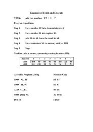
Latches and Flip Flops
Latches and Flip Flops
Latches and Flip Flops

Create successful ePaper yourself
Turn your PDF publications into a flip-book with our unique Google optimized e-Paper software.
<strong>Flip</strong> <strong>Flops</strong><br />
@ P. Klimo<br />
<strong>Latches</strong> <strong>and</strong> <strong>Flip</strong> <strong>Flops</strong><br />
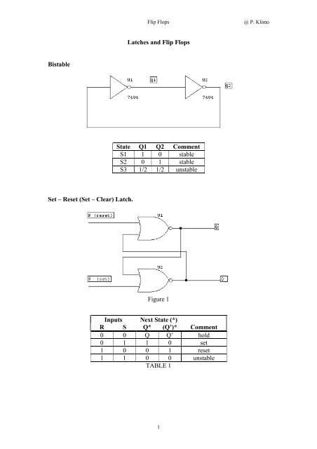
Bistable<br />
State Q1 Q2 Comment<br />
S1 1 0 stable<br />
S2 0 1 stable<br />
S3 1/2 1/2 unstable<br />
Set – Reset (Set – Clear) Latch.<br />
Figure 1<br />
Inputs Next State (*)<br />
R S Q* (Q’)* Comment<br />
0 0 Q Q’ hold<br />
0 1 1 0 set<br />
1 0 0 1 reset<br />
1 1 0 0 unstable<br />
TABLE 1<br />
1
<strong>Flip</strong> <strong>Flops</strong><br />
@ P. Klimo<br />
Excerxise: R-S Latch with Low Asserted Inputs.<br />
Design a sequential circuit which is described by the following Next State table:<br />
Base your design on NAND gates.<br />
Solution:<br />
Inputs Next State (*)<br />
R S Q* (Q’)* Comment<br />
1 1 Q Q’ hold<br />
1 0 1 0 set<br />
0 1 0 1 reset<br />
0 0 0 0 unstable<br />
TABLE 2<br />
Step 1: Implement as a combinatorial circuit with a (single) feedback loop:<br />
Step 2: Break the feedback loop <strong>and</strong> analyse the transition from the present state Q to<br />
the next state Q*:<br />
Step 3: Draw the K map for output Q* in terms of inputs R, S <strong>and</strong> Q:<br />
INPUTS<br />
Q R S<br />
00 01 11 10<br />
0 X 0 0 1<br />
1 X 0 1 1<br />
K-map for Q*<br />
2
<strong>Flip</strong> <strong>Flops</strong><br />
@ P. Klimo<br />
Step 4: Solve the K map to obtain the so called characteristic equation :<br />
Q* = Q.R + S’<br />
Step 5: Implement the characteristic equation using NAND gates:<br />
Q* = Q.R + S’ = ( (Q.R)’ .S )’<br />
Figure 2: R S Latch with low asserted inputs.<br />
Characteristic Equation of R-S Latch : Expresses the next state Q* as a function of<br />
the present state Q <strong>and</strong> of the inputs (R <strong>and</strong> S).<br />
Q* = (forcing term) + Q. (holding term)<br />
Q* = S’ + Q .R<br />
Exercise: Derive the characteristic equations for the R-S latch in figure 1.<br />
Answer: Q* = S+R’. Q<br />
Excitation Map for R-S Latch: Given a state transition Q -> Q*, the excitation<br />
map shows the combination of R <strong>and</strong> S inputs which are required to produce it.<br />
Current State Next State Required Inputs<br />
Q Q* R S<br />
______________________________________________<br />
0 0 X 0<br />
0 1 0 1<br />
1 1 0 X<br />
1 0 1 0<br />
3
<strong>Flip</strong> <strong>Flops</strong><br />
@ P. Klimo<br />
D (Data) Latch.<br />
Figure 3: Implementation of D latch.<br />
Characteristic equation of D latch :<br />
Q* = D<br />
D Latch with Enable (transparent latch):<br />
Inputs Next State (*)<br />
D E Q* Comment<br />
0 0 Q n<br />
hold<br />
1 0 Q n<br />
hold<br />
0 1 0<br />
reset<br />
1 1 1 set<br />
TABLE 3.<br />
Example: Design of D Latch with Enable.<br />
Draw a K map for Table 3:<br />
D E<br />
Q 0 0 0 1 1 1 1 0<br />
0 0 0 1 0<br />
1 1 0 1 1<br />
Figure 4: K-map for Q*<br />
Characteristic Equation of transparent D latch: Q* = D.E + E’.Q<br />
4
<strong>Flip</strong> <strong>Flops</strong><br />
@ P. Klimo<br />
Excitation map:<br />
Current State Next State Required Inputs<br />
Q Q* D E<br />
______________________________________________<br />
0 0 X 0<br />
0 1 1 1<br />
1 1 X 0<br />
1 0 0 1<br />
Implementation of transparent D latch.<br />
Figure 5 : D-Latch with Enable.<br />
5
<strong>Flip</strong> <strong>Flops</strong><br />
@ P. Klimo<br />
Propagation Delays <strong>and</strong> Static Hazards:<br />
Single Gate Propagation Delay t pd : time delay (in nS) between gate output reaction<br />
to the input change. (Sometimes t pd is specified separately for low to high <strong>and</strong> high to<br />
low transitions.)<br />
Example:<br />
Figure 6: Cascaded XOR Gates.<br />
Figure 7: Time Diagram of Cascaded XOR Gates.<br />
Circuit in figure 5 shows that the implementation experiences a static 0 hazard on the<br />
output. According to Boolean law the OUT should always remain low, but because of<br />
the t pd (10 nS) of the XOR gates a high glitch will appear.<br />
Figure 8: Improved design produces no glitch.<br />
6
<strong>Flip</strong> <strong>Flops</strong><br />
@ P. Klimo<br />
Example:<br />
The D Latch with enable, as implemented in figure 5, also produces a glitch.<br />
Assume Q = D =1 <strong>and</strong> E changes from 1 to 0. The output should remain high.<br />
However, because of the propagation delay introduced by the inverter, the output of<br />
the upper AND goes low before the output of the lower AND goes high. So the Q<br />
output swings low <strong>and</strong> because of the feedback loop it stays low. This is a so called<br />
static hazard one.<br />
E D<br />
Q 0 0 0 1 1 1 1 0<br />
0 0 0 1 0<br />
1 1 1 1 0<br />
Looking at the K-map of the D latch in figure 4 (reproduced above) one observes that<br />
the possibility of a hazard one arises for the transitions across the boundary between<br />
the two prime implicants E.D <strong>and</strong> E’.Q when Q=1 (bottom row).<br />
.<br />
To overcome the static hazard introduce an extra AND gate to cover the transition<br />
between the cells indicated by the arrows. This requires an additional term D.Q:<br />
Q* = E.D + E’.Q + D.Q<br />
Figure 9: Improved D Latch with enable.<br />
7
<strong>Flip</strong> <strong>Flops</strong><br />
@ P. Klimo<br />
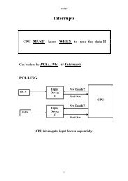
<strong>Flip</strong> <strong>Flops</strong> (FF) – Synchronous Devices.<br />
With FF, the transitions to the next state are synchronised with a clock (rising or<br />
falling ) edges.<br />
D <strong>Flip</strong> Flop:<br />
Figure 10: Symbol of a Negative (or Falling) Edge D <strong>Flip</strong>-Flop<br />
Figure 11: Implementation of a Negative Edge Master-Slave D <strong>Flip</strong>-Flop.<br />
Timing Diagram of the M-S D <strong>Flip</strong>-Flop<br />
8
<strong>Flip</strong> <strong>Flops</strong><br />
@ P. Klimo<br />
Figure 12: Implementation of D <strong>Flip</strong>-Flop using a Pulse Transition Detector.<br />
R-S <strong>Flip</strong> Flop:<br />
Figure 13: Pulse Transition Detector.<br />
Figure 14: Symbol for a Falling Edge R-S <strong>Flip</strong>-Flop<br />
Figure 15: Implementation of a Master Slave RS FF.<br />
9
<strong>Flip</strong> <strong>Flops</strong><br />
@ P. Klimo<br />
JK <strong>Flip</strong> Flop:<br />
Figure 16: Implementation of RS latch using Pulse Transition Detector<br />
Figure 17: Symbol for a Positive (Rising) Edge JK <strong>Flip</strong>-Flop<br />
Description of JK <strong>Flip</strong>-Flop Behaviour.<br />
J K Q* Mode<br />
0 0 Q hold<br />
0 1 0 reset<br />
1 0 1 set<br />
1 1 Q’ toggle<br />
Truth Table for JK <strong>Flip</strong> Flop<br />
10
<strong>Flip</strong> <strong>Flops</strong><br />
@ P. Klimo<br />
Next State Diagram for JK <strong>Flip</strong> Flop.<br />
Present<br />
State<br />
Inputs<br />
Next<br />
State<br />
Q J K Q*<br />
0 0 0 0<br />
1 0 0 1<br />
0 1 0 1<br />
1 1 0 1<br />
0 0 1 0<br />
1 0 1 0<br />
0 1 1 1<br />
1 1 1 0<br />
Next State Table for JK <strong>Flip</strong> Flop.<br />
Characteristic equation of JK <strong>Flip</strong> Flop:<br />
Q* = J.Q’ + K’.Q<br />
Homework: derive the above equation from the Next State Table.<br />
Transition Req. inputs<br />
Q -> Q* J K<br />
0 0 0 X<br />
0 1 1 X<br />
1 1 X 0<br />
1 0 X 1<br />
Excitation map for JK flip flop<br />
11
<strong>Flip</strong> <strong>Flops</strong><br />
@ P. Klimo<br />
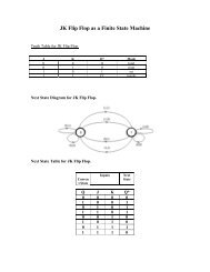
Exercise: Implementation of JK <strong>Flip</strong> Flop using a RS <strong>Flip</strong> Flop<br />
Block Diagram.<br />
Figure 18: JK <strong>Flip</strong>-Flop as a Finite State Machine<br />
Next State Logic:<br />
K - Map for S:<br />
Q<br />
J K 0 1<br />
0 0 0 0<br />
0 1 0 0<br />
1 1 1 0<br />
1 0 1 0<br />
S = J.Q’<br />
K-Map for R:<br />
Q<br />
J K 0 1<br />
0 0 0 0<br />
0 1 0 0<br />
1 1 1 0<br />
1 0 1 0<br />
R = K.Q<br />
Figure 19: A realisation of J K <strong>Flip</strong> Flop using a RS <strong>Flip</strong> Flop<br />
12
<strong>Flip</strong> <strong>Flops</strong><br />
@ P. Klimo<br />
Timing Definitions for (Negative) Clock Edge Operation<br />
Synchronous inputs have to be stable for a minimum time t s – set up time before the<br />
arrival of the clock edge <strong>and</strong> remain stable for a a duration t h – hold up time.<br />
Asynchronous inputs (set <strong>and</strong> reset) override the clock.<br />
Figure 20: Definition of Set-up <strong>and</strong> Hold times.<br />
13