Unit – 3 Session - 12 Data Processing Circuits - VTU e-Learning ...
Unit – 3 Session - 12 Data Processing Circuits - VTU e-Learning ...
Unit – 3 Session - 12 Data Processing Circuits - VTU e-Learning ...

Create successful ePaper yourself
Turn your PDF publications into a flip-book with our unique Google optimized e-Paper software.
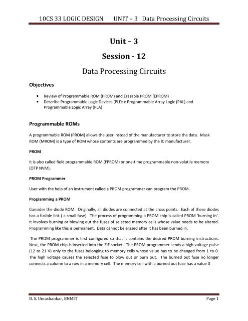
10CS 33 LOGIC DESIGN<br />
UNIT <strong>–</strong> 3 <strong>Data</strong> <strong>Processing</strong> <strong>Circuits</strong><br />
<strong>Unit</strong> <strong>–</strong> 3<br />
<strong>Session</strong> - <strong>12</strong><br />
<strong>Data</strong> <strong>Processing</strong> <strong>Circuits</strong><br />
Objectives<br />
• Review of Programmable ROM (PROM) and Erasable PROM (EPROM)<br />
• Describe Programmable Logic Devices (PLDs): Programmable Array Logic (PAL) and<br />
Programmable Logic Array (PLA)<br />
Programmable ROMs<br />
A programmable ROM (PROM) allows the user instead of the manufacturer to store the data. Mask<br />
ROM (MROM) is a type of ROM whose contents are programmed by the IC manufacturer.<br />
PROM<br />
It is also called field programmable ROM (FPROM) or one-time programmable non-volatile memory<br />
(OTP NVM).<br />
PROM Programmer<br />
User with the help of an instrument called a PROM programmer can program the PROM.<br />
Programming a PROM<br />
Consider the diode ROM. Originally, all diodes are connected at the cross points. Each of these diodes<br />
has a fusible link ( a small fuse). The process of programming a PROM chip is called PROM ‘burning in’.<br />
It involves burning or blowing out the fuses of selected memory cells whose value needs to be altered.<br />
Programming like this is permanent. <strong>Data</strong> cannot be erased after it has been burned in.<br />
The PROM programmer is first configured so that it contains the desired PROM burning instructions.<br />
Next, the PROM chip is inserted into the ZIF socket. The PROM programmer sends a high voltage pulse<br />
(<strong>12</strong> to 21 V) only to the fuses belonging to memory cells whose value has to be changed from 1 to 0.<br />
The high voltage causes the selected fuse to blow out or burn out. The burned out fuse no longer<br />
connects a column to a row in a memory cell. The memory cell with a burned out fuse has a value 0<br />
B. S. Umashankar, BNMIT Page 1
10CS 33 LOGIC DESIGN<br />
UNIT <strong>–</strong> 3 <strong>Data</strong> <strong>Processing</strong> <strong>Circuits</strong><br />
Disadvantage of PROM<br />
There is a limit on the number of input variables. Typically, PROMs have 8 inputs or less.<br />
Drawing a PROM logic circuit<br />
It is cumbersome to draw large PROM circuit with all the diodes. An alternative, streamlined drawing<br />
procedure for PROMs is used. The simplified diagram of PROM is as shown:<br />
Universal Logic Solution<br />
PROM is an universal logic solution. The AND gates generate all the fundamental products and the user<br />
can then OR these products as needed to generate any Boolean output.<br />
Example:<br />
Realize a full adder using a PROM.<br />
Solution:<br />
The truth table of the full adder is as shown:<br />
B. S. Umashankar, BNMIT Page 2
10CS 33 LOGIC DESIGN<br />
UNIT <strong>–</strong> 3 <strong>Data</strong> <strong>Processing</strong> <strong>Circuits</strong><br />
Inputs<br />
Outputs<br />
A B Ci S Co<br />
0 0 0 0 0<br />
0 0 1 1 0<br />
0 1 0 1 0<br />
0 1 1 0 1<br />
1 0 0 1 0<br />
1 0 1 0 1<br />
1 1 0 0 1<br />
1 1 1 1 1<br />
The full adder using PROM is realized as shown below:<br />
Erasable PROMs<br />
The erasable PROM (EPROM) uses metal-oxide semiconductor field-effect effect transistors (MOSFETs). It has<br />
an array of floating-gate gate transistors individually programmed by an EPROM programmer. Storing data in<br />
the memory requires selecting a given address and applying a higher voltage to the transistors.<br />
Erasing EPROM contents<br />
B. S. Umashankar, BNMIT<br />
Page 3
10CS 33 LOGIC DESIGN<br />
UNIT <strong>–</strong> 3 <strong>Data</strong> <strong>Processing</strong> <strong>Circuits</strong><br />
The stored data is erased by exposing the die to ultraviolet (UV) light. The UV light passes through the<br />
quartz window in the IC package and releases all stored charges. The effect is to erase the stored<br />
contents.<br />
EPROM ICs<br />
Some important EPROM IC types are listed below:<br />
2716 16 K bits organized as 2048 x 8 (2 KB)<br />
2732 32 K bits organized as 4096 x 8 (4 KB)<br />
27256 256 K bits organized as 32768 x 8 (32 KB)<br />
Importance of EPROM<br />
The EPROM is useful in project development. The designer can modify the contents until the stored<br />
data is perfect. When the design is finalized, the data can be burned into PROM.<br />
Programmable Array Logic<br />
Programmable Array Logic (PAL) is a programmable array of logic gates on a single chip. PAL is different<br />
from a PROM. It has a programmable AND array and a fixed OR array. The structure of PAL is as shown<br />
below:<br />
Programming a PAL<br />
With a PROM programmer, we can burn in the desired fundamental products, which are then ORed by<br />
the fixed output connections.<br />
B. S. Umashankar, BNMIT Page 4
10CS 33 LOGIC DESIGN<br />
UNIT <strong>–</strong> 3 <strong>Data</strong> <strong>Processing</strong> <strong>Circuits</strong><br />
Example:<br />
Realize a full adder using PAL.<br />
Solution:<br />
The output expressions of a full adder are:<br />
S = Σ m(1, 2, 4, 7)<br />
Co = Σ m(3, 5, 6, 7)<br />
Full adder is realized using PAL as shown below:<br />
PAL ICs<br />
Some important PAL IC types are listed below:<br />
10H8<br />
16H2<br />
14L4<br />
10 input and 8 output AND-OR<br />
6 input and 2 output AND-OR<br />
14 input and 4 output AND-OR-INVERT<br />
B. S. Umashankar, BNMIT<br />
Page 5
10CS 33 LOGIC DESIGN<br />
UNIT <strong>–</strong> 3 <strong>Data</strong> <strong>Processing</strong> <strong>Circuits</strong><br />
PAL - Pros and Cons<br />
PALs are not an universal logic solution. Only some of the fundamental products can be generated and<br />
ORed at the final outputs. But PALs have enough flexibility to produce all kinds of complicated logic<br />
functions. PALs have the advantage of 16 inputs compared to the typical limit of 8 inputs for PROMs.<br />
Programmable Logic Arrays<br />
In Programmable Logic Arrays (PLAs) both the AND array and the OR array are programmable. PLAs<br />
along with ROMs and PALs, are included in the more general classification of ICs called programmable<br />
logic devices (PLDs).<br />
PLDs<br />
The block diagrams of the three PLDs are as shown below:<br />
B. S. Umashankar, BNMIT<br />
Page 6
10CS 33 LOGIC DESIGN<br />
UNIT <strong>–</strong> 3 <strong>Data</strong> <strong>Processing</strong> <strong>Circuits</strong><br />
The structure of Programmable Logic Array (PLA) is as shown below:<br />
We can use PLA for combinational logic circuit design.<br />
Example:<br />
Realize a 7-segment decoder using PLA.<br />
Solution:<br />
The truth table of 7-segment decoder is as shown:<br />
B. S. Umashankar, BNMIT<br />
Page 7
10CS 33 LOGIC DESIGN<br />
UNIT <strong>–</strong> 3 <strong>Data</strong> <strong>Processing</strong> <strong>Circuits</strong><br />
BCD Input<br />
Outputs<br />
A B C D a b c d e f g<br />
0 0 0 0 1 1 1 1 1 1 0<br />
0 0 0 1 0 1 1 0 0 0 0<br />
0 0 1 0 1 1 0 1 1 0 1<br />
0 0<br />
0 1<br />
0 1<br />
0 1<br />
0 1<br />
1 0<br />
1 0<br />
1 1 1 1 1 1 0 0 1<br />
0 0 0 1 1 0 0 1 1<br />
0 1 1 0 1 1 0 1 1<br />
1 0 1 0 1 1 1 1 1<br />
1 1 1 1 1 0 0 0 0<br />
0 0 1 1 1 1 1 1 1<br />
0 1 1 1 1 0 0 1 1<br />
The 7-segment decoder is realized using PLA as shown below:<br />
B. S. Umashankar, BNMIT<br />
Page 8
10CS 33 LOGIC DESIGN<br />
UNIT <strong>–</strong> 3 <strong>Data</strong> <strong>Processing</strong> <strong>Circuits</strong><br />
Questions<br />
1. Mention different types of ROMs and explain each of them.<br />
2. Implement the following Boolean functions using an appropriate PLA:<br />
F1(A, B, C) = ∑m(0, 4, 7); F2 (A, B, C) = ∑m(4, 6).<br />
3. What are the different types of PLDs? Implement the 7-segment decoder using PLA.<br />
4. Implement the following function using PLA:<br />
X = A’B’C + AB’C’ + B’C; Y = A’B’C + AB’C’; Z = B’C<br />
B. S. Umashankar, BNMIT Page 9