6N138, 6N139 Dual-Channel - Fairchild Semiconductor
6N138, 6N139 Dual-Channel - Fairchild Semiconductor
6N138, 6N139 Dual-Channel - Fairchild Semiconductor

Create successful ePaper yourself
Turn your PDF publications into a flip-book with our unique Google optimized e-Paper software.
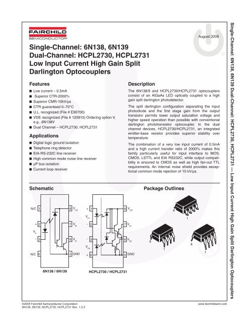
Single-<strong>Channel</strong>: <strong>6N138</strong>, <strong>6N139</strong><br />
<strong>Dual</strong>-<strong>Channel</strong>: HCPL2730, HCPL2731<br />
Low Input Current High Gain Split<br />
Darlington Optocouplers<br />
Features<br />
■ Low current – 0.5mA<br />
■ Superior CTR-2000%<br />
■ Superior CMR-10kV/µs<br />
■ CTR guaranteed 0–70°C<br />
■ U.L. recognized (File # E90700)<br />
■ VDE recognized (File # 120915) Ordering option V,<br />
e.g., <strong>6N138</strong>V<br />
■ <strong>Dual</strong> <strong>Channel</strong> – HCPL2730, HCPL2731<br />
Applications<br />
■ Digital logic ground isolation<br />
■ Telephone ring detector<br />
■ EIA-RS-232C line receiver<br />
■ High common mode noise line receiver<br />
■ µP bus isolation<br />
■ Current loop receiver<br />
Schematic<br />
N/C<br />
1<br />
+ 2<br />
V F<br />
_<br />
3<br />
8<br />
7<br />
6<br />
V CC<br />
V B<br />
V O<br />
N/C 4 5 GND<br />
<strong>6N138</strong> / <strong>6N139</strong><br />
+<br />
V F1<br />
_<br />
_<br />
V F2<br />
1<br />
2<br />
3<br />
+ 4 5 GND<br />
HCPL2730 / HCPL2731<br />
8<br />
7<br />
6<br />
Description<br />
August 2008<br />
The <strong>6N138</strong>/9 and HCPL2730/HCPL2731 optocouplers<br />
consist of an AlGaAs LED optically coupled to a high<br />
gain split darlington photodetector.<br />
The split darlington configuration separating the input<br />
photodiode and the first stage gain from the output<br />
transistor permits lower output saturation voltage and<br />
higher speed operation than possible with conventional<br />
darlington phototransistor optocoupler. In the dual<br />
channel devices, HCPL2730/HCPL2731, an integrated<br />
emitter-base resistor provides superior stability over<br />
temperature.<br />
The combination of a very low input current of 0.5mA<br />
and a high current transfer ratio of 2000% makes this<br />
family particularly useful for input interface to MOS,<br />
CMOS, LSTTL and EIA RS232C, while output compatibility<br />
is ensured to CMOS as well as high fan-out TTL<br />
requirements. An internal noise shield provides exceptional<br />
common mode rejection of 10 kV/µs.<br />
V CC<br />
V 01<br />
V 02<br />
Package Outlines<br />
8<br />
1<br />
8<br />
1<br />
8<br />
1<br />
Single-<strong>Channel</strong>: <strong>6N138</strong>, <strong>6N139</strong> <strong>Dual</strong>-<strong>Channel</strong>: HCPL2730, HCPL2731 — Low Input Current High Gain Split Darlington Optocouplers<br />
©2005 <strong>Fairchild</strong> <strong>Semiconductor</strong> Corporation www.fairchildsemi.com<br />
<strong>6N138</strong>, 5N139, NCPL2730, HCPL2731 Rev. 1.0.5
Absolute Maximum Ratings (T A = 25°C unless otherwise specified)<br />
Stresses exceeding the absolute maximum ratings may damage the device. The device may not function or be<br />
operable above the recommended operating conditions and stressing the parts to these levels is not recommended.<br />
In addition, extended exposure to stresses above the recommended operating conditions may affect device reliability.<br />
The absolute maximum ratings are stress ratings only.<br />
Symbol Parameter Value Units<br />
T STG Storage Temperature -55 to +125 °C<br />
T OPR Operating Temperature -40 to +85 °C<br />
T SOL Lead Solder Temperature (Wave solder only. See recommended reflow profile<br />
graph for SMD mounting)<br />
260 for 10 sec °C<br />
EMITTER<br />
I F (avg) DC/Average Forward Input Current Each <strong>Channel</strong> 20 mA<br />
I F (pk) Peak Forward Input Current (50% duty cycle, 1 ms P.W.) Each <strong>Channel</strong> 40 mA<br />
I F (trans) Peak Transient Input Current - (≤1µs P.W., 300 pps) 1.0 A<br />
V R Reverse Input Voltage Each <strong>Channel</strong> 5 V<br />
P D Input Power Dissipation Each <strong>Channel</strong> 35 mW<br />
DETECTOR<br />
I O (avg) Average Output Current Each <strong>Channel</strong> 60 mA<br />
V ER Emitter-Base Reverse Voltage <strong>6N138</strong> and <strong>6N139</strong> 0.5 V<br />
V CC , V O Supply Voltage, Output Voltage <strong>6N138</strong>, HCPL2730 -0.5 to 7 V<br />
<strong>6N139</strong>, HCPL2731 -0.5 to 18<br />
P O Output Power Dissipation Each <strong>Channel</strong> 100 mW<br />
Single-<strong>Channel</strong>: <strong>6N138</strong>, <strong>6N139</strong> <strong>Dual</strong>-<strong>Channel</strong>: HCPL2730, HCPL2731 — Low Input Current High Gain Split Darlington Optocouplers<br />
©2005 <strong>Fairchild</strong> <strong>Semiconductor</strong> Corporation www.fairchildsemi.com<br />
<strong>6N138</strong>, 5N139, NCPL2730, HCPL2731 Rev. 1.0.5 2
Electrical Characteristics (T A = 0 to 70°C unless otherwise specified)<br />
Individual Component Characteristics<br />
Symbol Parameter Test Conditions Device Min. Typ.* Max. Unit<br />
EMITTER<br />
V F Input Forward Voltage T A = 25°C All 1.30 1.7 V<br />
Each channel (I F = 1.6mA) 1.75<br />
BV R Input Reverse<br />
Breakdown Voltage<br />
T A = 25°C, I R = 10µA All 5.0 20 V<br />
∆V F / ∆T A<br />
DETECTOR<br />
I OH<br />
Temperature<br />
Coefficient of<br />
Forward Voltage<br />
Logic HIGH Output<br />
Current<br />
Transfer Characteristics<br />
*All Typicals at T A = 25°C<br />
I F = 1.6mA All -1.8 mV/°C<br />
I F = 0mA, V O = V CC = 18V <strong>6N139</strong> 0.01 100 µA<br />
Each <strong>Channel</strong> HCPL2731<br />
I F = 0mA, V O = V CC = 7V <strong>6N138</strong> 0.01 250<br />
Each <strong>Channel</strong> HCPL2730<br />
I CCL Logic LOW supply I F = 1.6mA, V O = Open, V CC = 18V <strong>6N138</strong>,<br />
0.4 1.5 mA<br />
<strong>6N139</strong><br />
I F1 = I F2 = 1.6mA, V CC = 18V HCPL2731 1.3 3<br />
V O1 – V O2 = Open, V CC = 7V<br />
HCPL2730<br />
I CCH Logic HIGH Supply I F = 0mA, V O = Open, V CC = 18V <strong>6N138</strong>,<br />
0.05 10 µA<br />
<strong>6N139</strong><br />
I F1 = I F2 = 0mA, V CC = 18V HCPL2731 0.10 20<br />
V O1 – V O2 = Open, V CC = 7V<br />
HCPL2730<br />
Symbol Parameter Test Conditions Device Min. Typ.* Max. Unit<br />
I = 0.5mA, V = 0.4 V, V = 4.5V <strong>6N139</strong> 400 1100 %<br />
I = 0.5mA, I = 2mA, V = 4.5V <strong>6N139</strong> 0.08 0.4 V<br />
COUPLED<br />
CTR Current Transfer<br />
Ratio (1)(2) F O CC<br />
Each <strong>Channel</strong> HCPL2731 3500<br />
I F = 1.6mA, V O = 0.4 V, V CC = 4.5V <strong>6N139</strong> 500 1300<br />
Each <strong>Channel</strong> HCPL2731 2500<br />
I F = 1.6mA, V O = 0.4 V, V CC = 4.5V <strong>6N138</strong> 300 1300<br />
Each <strong>Channel</strong> HCPL2730 2500<br />
V OL Logic LOW Output<br />
Voltage (2) F O CC<br />
I F = 1.6mA, I O = 8mA, V CC = 4.5V <strong>6N139</strong> 0.01 0.4<br />
Each <strong>Channel</strong> HCPL2731<br />
I F = 0.5mA, I O = 15mA, V CC = 4.5V <strong>6N139</strong> 0.13 0.4<br />
Each <strong>Channel</strong> HCPL2731<br />
I F = 12mA, I O = 24mA, V CC = 4.5V <strong>6N139</strong> 0.20 0.4<br />
Each <strong>Channel</strong> HCPL2731<br />
I F = 1.6mA, I O = 4.8mA, V CC = 4.5V <strong>6N138</strong> 0.10 0.4<br />
Each <strong>Channel</strong> HCPL2730<br />
Single-<strong>Channel</strong>: <strong>6N138</strong>, <strong>6N139</strong> <strong>Dual</strong>-<strong>Channel</strong>: HCPL2730, HCPL2731 — Low Input Current High Gain Split Darlington Optocouplers<br />
©2005 <strong>Fairchild</strong> <strong>Semiconductor</strong> Corporation www.fairchildsemi.com<br />
<strong>6N138</strong>, 5N139, NCPL2730, HCPL2731 Rev. 1.0.5 3
Electrical Characteristics (Continued) (T A = 0 to 70°C unless otherwise specified)<br />
Switching Characteristics (V CC = 5V)<br />
Symbol Parameter Test Conditions Device Min. Typ.* Max. Unit<br />
T PHL<br />
T PLH<br />
|CM H |<br />
|CM L |<br />
Propagation Delay<br />
Time to Logic<br />
LOW (2) (Fig. 24)<br />
Propagation Delay<br />
Time to Logic<br />
HIGH (2) (Fig. 24)<br />
Common Mode<br />
Transient<br />
Immunity at Logic<br />
HIGH (3) (Fig. 25)<br />
Common Mode<br />
Transient<br />
Immunity at Logic<br />
LOW (3) (Fig. 25)<br />
** All Typicals at T A = 25°C<br />
R L = 4.7Ω, I F = 0.5mA <strong>6N139</strong> 30 µs<br />
T A = 25°C 4 25<br />
R L = 4.7Ω, I F = 0.5mA HCPL2731 120<br />
Each <strong>Channel</strong> T A = 25°C 3 100<br />
R L = 270Ω, I F = 12mA <strong>6N139</strong> 2<br />
T A = 25°C 0.2 1<br />
R L = 270Ω, I F = 12mA, Each <strong>Channel</strong> HCPL2730 3<br />
T A = 25°C HCPL2731 0.3 2<br />
R L = 2.2Ω, I F = 1.6mA <strong>6N138</strong> 15<br />
T A = 25°C 1.5 10<br />
R L = 2.2Ω, I F = 1.6mA, Each <strong>Channel</strong> HCPL2731<br />
25<br />
T A = 25°C<br />
HCPL2730<br />
1 20<br />
R L = 4.7Ω, I F = 0.5mA <strong>6N139</strong> 90 µs<br />
Each <strong>Channel</strong> HCPL2731<br />
R L = 4.7Ω, I F = 0.5mA, T A = 25°C <strong>6N139</strong> 12 60<br />
Each <strong>Channel</strong> HCPL2731 22<br />
R L = 270Ω, I F = 12mA <strong>6N139</strong> 10<br />
T A = 25°C 1.3 7<br />
R L = 270Ω, I F = 12mA, Each <strong>Channel</strong> HCPL2730<br />
15<br />
T A = 25°C<br />
HCPL2731<br />
5 10<br />
R L = 2.2Ω, I F = 1.6mA <strong>6N138</strong> 50<br />
Each <strong>Channel</strong> HCPL2730/1<br />
R L = 2.2Ω, I F = 1.6mA, T A = 25°C <strong>6N138</strong> 7 35<br />
Each <strong>Channel</strong> HCPL2730/1 16<br />
I F = 0mA, |V CM | = 10V P-P , T A = 25°C,<br />
R L = 2.2Ω<br />
Each <strong>Channel</strong><br />
(I F = 1.6mA, |V CM | = 10V P-P , R L = 2.2Ω)<br />
T A = 25°C<br />
Each <strong>Channel</strong><br />
<strong>6N138</strong><br />
<strong>6N139</strong><br />
HCPL2730<br />
HCPL2731<br />
<strong>6N138</strong><br />
<strong>6N139</strong><br />
HCPL2730<br />
HCPL2731<br />
1,000 10,000 V/µs<br />
1,000 10,000 V/µs<br />
Single-<strong>Channel</strong>: <strong>6N138</strong>, <strong>6N139</strong> <strong>Dual</strong>-<strong>Channel</strong>: HCPL2730, HCPL2731 — Low Input Current High Gain Split Darlington Optocouplers<br />
©2005 <strong>Fairchild</strong> <strong>Semiconductor</strong> Corporation www.fairchildsemi.com<br />
<strong>6N138</strong>, 5N139, NCPL2730, HCPL2731 Rev. 1.0.5 4
Electrical Characteristics (Continued) (T A = 0 to 70°C unless otherwise specified)<br />
Isolation Characteristics<br />
Symbol Characteristics Test Conditions Min. Typ.* Max. Unit<br />
*All Typicals at T A = 25°C<br />
Notes:<br />
1. Current Transfer Ratio is defined as a ratio of output collector current, I O , to the forward LED input current,<br />
I F , times 100%.<br />
2. Pin 7 open. (<strong>6N138</strong> and <strong>6N139</strong> only)<br />
3. Common mode transient immunity in logic HIGH level is the maximum tolerable (positive) dV cm /dt on the<br />
leading edge of the common mode pulse signal V CM , to assure that the output will remain in a logic HIGH state<br />
(i.e., V O > 2.0V). Common mode transient immunity in logic LOW level is the maximum tolerable (negative)<br />
dV cm /dt on the trailing edge of the<br />
common mode pulse signal, V CM , to assure that the output will remain in a logic LOW state (i.e., V O < 0.8V).<br />
4. Device is considered a two terminal device: Pins 1, 2, 3 and 4 are shorted together and Pins 5, 6, 7 and 8 are<br />
shorted together.<br />
5. For dual channel devices, C I-O is measured by shorting pins 1 and 2 or pins 3 and 4 together and pins 5 through 8<br />
shorted together.<br />
6. Measured between pins 1 and 2 shorted together, and pins 3 and 4 shorted together.<br />
I<br />
I I-O<br />
V ISO<br />
Input-Output Insulation Leakage<br />
Current (4)<br />
Withstand Insulation Test<br />
Voltage (4)<br />
Relative humidity = 45%,T A = 25°C,<br />
t = 5s, V I-O = 3000VDC<br />
RH ≤ 50%, T A = 25°C, I I-O ≤ 2µA,<br />
t = 1 min.<br />
1.0 µA<br />
2500 V RMS<br />
R I-O Resistance (Input to Output) (4) V I-O = 500VDC 10 12 Ω<br />
C I-O Capacitance (Input to Output) (4)(5) f = 1MHz 0.6 pF<br />
I I-I Input-Input Insulation Leakage RH ≤ 45%, V I-I = 500VDC, t = 5s,<br />
0.005 µA<br />
Current (6) HCPL2730/2731 only<br />
R I-I Input-Input Resistance (6) V I-I = 500VDC, HCPL2730/2731 only 10 11 Ω<br />
C I-I Input-Input Capacitance (6) f = 1MHz, HCPL2730/2731 only 0.03 pF<br />
Single-<strong>Channel</strong>: <strong>6N138</strong>, <strong>6N139</strong> <strong>Dual</strong>-<strong>Channel</strong>: HCPL2730, HCPL2731 — Low Input Current High Gain Split Darlington Optocouplers<br />
©2005 <strong>Fairchild</strong> <strong>Semiconductor</strong> Corporation www.fairchildsemi.com<br />
<strong>6N138</strong>, 5N139, NCPL2730, HCPL2731 Rev. 1.0.5 5
Electrical Characteristics (Continued) T A = 25°C unless otherwise specified)<br />
Current Limiting Resistor Calculations<br />
R 1 (Non-Invert) = V DD1 – V DF – V OL1<br />
I F<br />
R 1 (Invert) = V DD1 – V OH1 – V DF<br />
I F<br />
R 2 = V DD2 = V OLX (@ I L – I 2 )<br />
I L<br />
Where:<br />
V DD1 = Input Supply Voltage<br />
V DD2 = Output Supply Voltage<br />
V DF = Diode Forward Voltage<br />
V OL1 = Logic “0” Voltage of Driver<br />
V OH1 = Logic “1” Voltage of Driver<br />
I F = Diode Forward Current<br />
V OLX = Saturation Voltage of<br />
Output Transistor<br />
I L = Load Current Through<br />
Resistor R2<br />
I 2 = Input Current of Output Gate<br />
IN<br />
V DD1<br />
R 1<br />
1<br />
2<br />
3<br />
4<br />
Fig. 2 Non-Inverting Logic Interface<br />
8<br />
7<br />
6<br />
5<br />
CMOS<br />
@ 5V<br />
V DD2<br />
R 2<br />
INPUT<br />
OUT<br />
R1 (V)<br />
IN<br />
CMOS<br />
@ 5V<br />
Fig. 1 Resistor Values for Logic Interface<br />
R 1<br />
CMOS<br />
@ 10V<br />
1 8<br />
2<br />
3<br />
4<br />
OUTPUT<br />
74XX 74LXX 74SXX 74LSXX 74HXX<br />
R2 (V) R2 (V) R2 (V) R2 (V) R2 (V) R2 (V) R2 (V)<br />
NON-INV. 2000 1000 2200 750 1000 1000 1000 560<br />
INV. 510<br />
CMOS NON-INV. 5100<br />
@ 10V<br />
INV. 4700<br />
74XX NON-INV. 2200<br />
INV. 180<br />
74LXX NON-INV. 1800<br />
INV. 100<br />
74SXX NON-INV. 2000<br />
INV. 360<br />
74LSXX NON-INV. 2000<br />
INV. 180<br />
74HXX NON-INV. 2000<br />
INV. 180<br />
Fig. 3 Inverting Logic Interface<br />
7<br />
6<br />
5<br />
V DD2<br />
R 2<br />
OUT<br />
Single-<strong>Channel</strong>: <strong>6N138</strong>, <strong>6N139</strong> <strong>Dual</strong>-<strong>Channel</strong>: HCPL2730, HCPL2731 — Low Input Current High Gain Split Darlington Optocouplers<br />
©2005 <strong>Fairchild</strong> <strong>Semiconductor</strong> Corporation www.fairchildsemi.com<br />
<strong>6N138</strong>, 5N139, NCPL2730, HCPL2731 Rev. 1.0.5 6
FORWARD CURRENT - IF (mA)<br />
TIME, T (µs)<br />
TIME - µs<br />
FORWARD VOLTAGE - VF (V)<br />
CURRENT TRANSFER RATIO - CTR (%)<br />
Typical Performance Curves<br />
TPHL - PROPAGATION DELAY TO LOGIC LOW - (µs)<br />
100<br />
0.01<br />
Fig. 4 LED Forward Current vs. Forward Voltage<br />
10<br />
1<br />
0.1<br />
T A = 70˚C<br />
T A = 85˚C<br />
T A = 25˚C<br />
T A = 0˚C<br />
T A = -40˚C<br />
0.001<br />
1.0 1.1 1.2 1.3 1.4 1.5 1.6<br />
100<br />
10<br />
FORWARD VOLTAGE - V F (V)<br />
Fig. 6 Non-saturated Rise and Fall Times vs.<br />
Load Resistance (<strong>6N138</strong> / <strong>6N139</strong> Only)<br />
1<br />
0.1 1 10<br />
6<br />
5<br />
4<br />
3<br />
2<br />
1<br />
T A = 25˚C<br />
I F ADJUSTED FOR V OL = 2 V<br />
R L - LOAD RESISTANCE (kΩ)<br />
Fig. 8 Propagation Delay To Logic Low<br />
vs. Base-Emitter Resistance<br />
(HCPL2730 / HCPL2731 Only)<br />
t f<br />
tr<br />
I F = 1.6 mA, V CC = 5 V<br />
R L = 2.2 K, T A = 25°C<br />
Normalized to R BE = None<br />
0<br />
0.01 0.1 1 10<br />
RBE - BASE-EMITTER RESISTANCE - MΩ<br />
1.5<br />
1.4<br />
1.3<br />
1.2<br />
1.1<br />
10<br />
1<br />
1600<br />
1200<br />
800<br />
400<br />
Fig. 5 LED Forward Voltage vs. Temperature<br />
I F = 1.6 mA<br />
-40 -20 0 20 40 60 80 100<br />
TEMPERATURE - T A (˚C)<br />
Fig. 7 Non-saturated Rise and Fall Times vs.<br />
Load Resistance (HCPL2730 / HCPL2731 Only)<br />
T A = 25˚C<br />
0.1 1 10<br />
R L - LOAD RESISTANCE (kΩ)<br />
Fig. 9 Current Transfer Ratio vs. Forward Current<br />
(<strong>6N138</strong> / <strong>6N139</strong> Only)<br />
V CC = 5V<br />
V O = 0.4V<br />
t r<br />
T A = 85˚C<br />
t f<br />
T A = -40˚C<br />
T A = 0˚C<br />
T A = 25˚C<br />
T A = 70˚C<br />
0<br />
0.01 0.1 1 10<br />
I F - FORWARD CURRENT - mA<br />
Single-<strong>Channel</strong>: <strong>6N138</strong>, <strong>6N139</strong> <strong>Dual</strong>-<strong>Channel</strong>: HCPL2730, HCPL2731 — Low Input Current High Gain Split Darlington Optocouplers<br />
©2005 <strong>Fairchild</strong> <strong>Semiconductor</strong> Corporation www.fairchildsemi.com<br />
<strong>6N138</strong>, 5N139, NCPL2730, HCPL2731 Rev. 1.0.5 7
CTR - CURRENT TRANSFER RATIO (%)<br />
IO-OUTPUT CURRENT -mA CTR - CURRENT TRANSFER RATIO (%)<br />
Typical Performance Curves (Continued)<br />
Fig. 10 Current Transfer Ratio vs. Base-Emitter Resistance<br />
(<strong>6N138</strong> / <strong>6N139</strong> Only)<br />
IO - OUTPUT CURRENT (mA)<br />
Fig. 14 Output Current vs. Input Diode Forward Current<br />
(<strong>6N138</strong> / <strong>6N139</strong> Only)<br />
IO - OUTPUT CURRENT (mA)<br />
1600<br />
1400<br />
1200<br />
1000<br />
800<br />
600<br />
400<br />
200<br />
60<br />
50<br />
40<br />
30<br />
20<br />
10<br />
100<br />
10<br />
1<br />
0<br />
Fig. 12 Output Current vs Output Voltage<br />
(<strong>6N138</strong> / <strong>6N139</strong> Only)<br />
V CC = 5V<br />
T A = 25˚C<br />
V CC = 5V<br />
V O = 0.4V<br />
T A = 85˚C<br />
R BE - BASE RESISTANCE (kΩ)<br />
T A = 25˚C<br />
T A = 0˚C<br />
T A = -40˚C<br />
5mA<br />
T A = 70˚C<br />
4.5mA<br />
4mA<br />
I F = 1.6mA<br />
V CC = 5 V<br />
V O = 0.4 V<br />
0<br />
1 10 100 1000<br />
3.5mA<br />
3mA<br />
2.5mA<br />
2mA<br />
1.5mA<br />
1mA<br />
0<br />
0 1 2<br />
V O - OUTPUT VOLTAGE (V)<br />
0<br />
0.01 0.1 1 10<br />
IF - INPUT DIODE FORWARD CURRENT -mA<br />
IO - OUTPUT CURRENT -mA<br />
Fig. 11 Current Transfer Ratio vs. Forward Current<br />
(HCPL2730 / HCPL2731 Only)<br />
5000<br />
4000<br />
3000<br />
2000<br />
1000<br />
120<br />
100<br />
80<br />
60<br />
40<br />
20<br />
100<br />
10<br />
1<br />
0.1<br />
V CC = 5 V<br />
V O = 0.4 V<br />
0<br />
0.1 1 10 100<br />
Fig. 13 Output Current vs Output Voltage<br />
(HCPL2730 / HCPL2731 Only)<br />
TA = 25˚C<br />
VCC = 5.0V<br />
IF = 4.0mA<br />
IF = 3.5mA<br />
0.0 0.2 0.4 0.6 0.8 1.0 1.2 1.4 1.6 1.8 2.0<br />
V O - OUTPUT VOLTAGE (V)<br />
V CC = 5.0V<br />
VO = 0.4V<br />
T A = 85˚C<br />
I F - FORWARD CURRENT -mA<br />
Fig. 15 Output Current vs<br />
Input Diode Forward Current<br />
(HCPL2730 / HCPL2731 Only)<br />
T A = -40˚C<br />
IF = 4.5mA<br />
T A = 25˚C<br />
T A = 70˚C<br />
T A = 85˚C<br />
T A = 25˚C<br />
T A = 0˚C<br />
T A = -40˚C<br />
IF = 5.0mA<br />
IF = 3.0mA<br />
IF = 2.5mA<br />
IF = 2.0mA<br />
IF = 1.5mA<br />
IF = 1.0mA<br />
IF = 0.5mA<br />
0.1 1 10 100<br />
IF - INPUT DIODE FORWARD CURRENT -mA<br />
Single-<strong>Channel</strong>: <strong>6N138</strong>, <strong>6N139</strong> <strong>Dual</strong>-<strong>Channel</strong>: HCPL2730, HCPL2731 — Low Input Current High Gain Split Darlington Optocouplers<br />
©2005 <strong>Fairchild</strong> <strong>Semiconductor</strong> Corporation www.fairchildsemi.com<br />
<strong>6N138</strong>, 5N139, NCPL2730, HCPL2731 Rev. 1.0.5 8
Typical Performance Curves (Continued)<br />
ICCL - LOGIC LOW SUPPLY CURRENT (mA)<br />
tP - PROPAGATION DELAY - µs<br />
tPHL - PROPAGATION DELAY to LOGIC LOW - µs<br />
4.0<br />
3.5<br />
3.0<br />
2.5<br />
2.0<br />
1.5<br />
1.0<br />
0.5<br />
0.0<br />
Fig. 18 Propagation Delay vs. Input Diode Forward Current<br />
(<strong>6N138</strong> / <strong>6N139</strong> Only)<br />
70<br />
60<br />
50<br />
40<br />
30<br />
20<br />
10<br />
0<br />
100<br />
10<br />
1<br />
V CC = 5 V<br />
T A = 25˚C<br />
Fig. 16 Logic Low Supply Current vs.<br />
Input Diode Forward Current<br />
(<strong>6N138</strong> / <strong>6N139</strong> Only)<br />
(t PHL ) R L = 2.2 kΩ or 4.7 kΩ<br />
V CC = 5V<br />
(t PLH ) R L = 4.7 kΩ<br />
(t PLH ) R L = 2.2 kΩ<br />
0 1 2 3 4 5 6 7 8 9 10<br />
I F - INPUT DIODE FORWARD CURRENT (mA)<br />
Fig. 20 Propagation Delay to Logic Low vs. Pulse Period<br />
(<strong>6N138</strong> / <strong>6N139</strong> Only)<br />
<strong>6N139</strong><br />
I F = 0.5mA<br />
R L = 4.7kΩ<br />
<strong>6N138</strong><br />
I F = 1.6mA<br />
R L = 2.2kΩ<br />
V CC = 18V<br />
0 2 4 6 8 10 12 14 16<br />
I F - FORWARD CURRENT (mA)<br />
T A = 25˚C<br />
0.1<br />
0.01 0.1 1 10<br />
T - INPUT PULSE PERIOD - ms<br />
ICCL - LOGIC LOW SUPPLY CURRENT - mA<br />
tP - PROPAGATION DELAY - µs<br />
tPHL - PROPAGATION DELAY to LOGIC LOW (µs)<br />
100<br />
10<br />
Fig. 19 Propagation Delay vs. Input Diode Forward Current<br />
(HCPL2730 / HCPL2731 Only)<br />
70<br />
60<br />
50<br />
40<br />
30<br />
20<br />
10<br />
100<br />
V CC = 5 V<br />
T A = 25˚C<br />
(t PHL ) R L = 2.2 kΩ or 4.7 kΩ<br />
(t PLH ) R L = 4.7 kΩ<br />
(t PLH ) R L = 2.2 kΩ<br />
0<br />
0 2 4 6 8 10<br />
10<br />
1<br />
1<br />
0.1<br />
Fig. 17 Logic Low Supply Current vs.<br />
Input Diode Forward Current<br />
(HCPL2730 / HCPL2731 Only)<br />
T A = 25˚C<br />
0.1 1 10 100<br />
I F - INPUT DIODE FORWARD CURRENT (mA)<br />
Fig. 21 Propagation Delay to Logic Low vs. Pulse Period<br />
(HCPL2730 / HCPL2731 Only)<br />
HCPL2731<br />
I F = 0.5mA<br />
R L = 4.7kΩ<br />
HCPL2731<br />
V CC = 18V<br />
I F - INPUT DIODE FORWARD CURRENT (mA)<br />
HCPL2730<br />
HCPL2731<br />
I F =1.6mA<br />
R L = 2.2kΩ<br />
HCPL2730<br />
HCPL2731<br />
V CC = 7V<br />
T A = 25˚C<br />
0.1<br />
0.01 0.1 1 10<br />
T - INPUT PULSE PERIOD - ms<br />
Single-<strong>Channel</strong>: <strong>6N138</strong>, <strong>6N139</strong> <strong>Dual</strong>-<strong>Channel</strong>: HCPL2730, HCPL2731 — Low Input Current High Gain Split Darlington Optocouplers<br />
©2005 <strong>Fairchild</strong> <strong>Semiconductor</strong> Corporation www.fairchildsemi.com<br />
<strong>6N138</strong>, 5N139, NCPL2730, HCPL2731 Rev. 1.0.5 9
Typical Performance Curves (Continued)<br />
tP - PROPAGATION DELAY (µs)<br />
50<br />
40<br />
30<br />
20<br />
10<br />
Fig. 22 Propagation Delay vs. Temperature<br />
(<strong>6N138</strong> / <strong>6N139</strong> Only)<br />
HCPL2730 : I F = 1.6 mA, R L = 2.2kΩ<br />
HCPL2731 : I F = 0.5 mA, R L = 4.7kΩ<br />
t PLH (HCPL2731)<br />
t PHL (HCPL2731)<br />
t PHL (HCPL2730)<br />
0<br />
0 10 20 30 40 50 60 70 80<br />
T A - TEMPERATURE (˚C)<br />
t PLH (HCPL2730)<br />
tP - PROPAGATION DELAY (µs)<br />
50<br />
40<br />
30<br />
20<br />
10<br />
Fig. 23 Propagation Delay vs. Temperature<br />
(HCPL2730 / HCPL2731 Only)<br />
HCPL2730 : I F = 1.6mA, R L = 2.2kΩ<br />
HCPL2731 : I F = 0.5mA, R L = 4.7kΩ<br />
t PLH (HCPL2731)<br />
t PHL (HCPL2731)<br />
t PHL (HCPL2730)<br />
0<br />
0 10 20 30 40 50 60 70 80<br />
T A - TEMPERATURE (˚C)<br />
t PLH (HCPL2730)<br />
Single-<strong>Channel</strong>: <strong>6N138</strong>, <strong>6N139</strong> <strong>Dual</strong>-<strong>Channel</strong>: HCPL2730, HCPL2731 — Low Input Current High Gain Split Darlington Optocouplers<br />
©2005 <strong>Fairchild</strong> <strong>Semiconductor</strong> Corporation www.fairchildsemi.com<br />
<strong>6N138</strong>, 5N139, NCPL2730, HCPL2731 Rev. 1.0.5 10
Test Circuits<br />
V FF<br />
Pulse<br />
Generator<br />
I<br />
tr = 5ns F<br />
Z O = 50 V<br />
10% D.C.<br />
I/ f< 100ns<br />
I Monitor<br />
F<br />
B<br />
R m<br />
V F<br />
1<br />
2<br />
3<br />
4<br />
I F<br />
2<br />
V F<br />
A<br />
3<br />
Noise<br />
1 Shield<br />
4<br />
Noise<br />
Shield<br />
+ -<br />
V CM<br />
Pulse Gen<br />
8<br />
7<br />
6<br />
Test Circuit for <strong>6N138</strong>, <strong>6N139</strong><br />
8<br />
7<br />
Test Circuit for <strong>6N138</strong> and <strong>6N139</strong><br />
V CC<br />
V B<br />
VO<br />
5 GND<br />
V CC<br />
V B<br />
V<br />
6 O<br />
5 GND<br />
R L<br />
0.1 µF<br />
I F<br />
V O<br />
R L<br />
0.1 µF<br />
V CM 10 V<br />
T PHL<br />
VO<br />
V O<br />
t r<br />
+5 V<br />
-<br />
+5 V<br />
V O<br />
C L = 15 pF*<br />
V O<br />
1.5 V<br />
90%<br />
Switch at A : I = 0 mA<br />
F<br />
Switch at B : I = 1.6 mA<br />
F<br />
Pulse<br />
Generator<br />
tr = 5ns<br />
Z O = 50V<br />
10% DUTY CYCLE<br />
I/f < 100 µS<br />
V FF<br />
IF<br />
MONITOR<br />
I F +<br />
1.5 V<br />
10% 10%<br />
0 V<br />
B<br />
I F<br />
A<br />
Rm<br />
VF1<br />
-<br />
VF2<br />
+<br />
TPLH<br />
+<br />
VF1<br />
-<br />
-<br />
VF2<br />
+<br />
1<br />
2<br />
3<br />
4 5<br />
V OL<br />
Fig. 24 Switching Time Test Circuit<br />
90%<br />
t f<br />
5 V<br />
V OL<br />
Noise<br />
Shield<br />
5 V<br />
V CM<br />
+ -<br />
Pulse Gen<br />
8<br />
7<br />
6<br />
VCC<br />
RL<br />
0.1 µF<br />
V01<br />
V02<br />
GND<br />
Test Circuit for HCPL2730 and HCPL2731<br />
1<br />
2<br />
3<br />
4<br />
Noise<br />
Shield<br />
Fig. 25 Common Mode Immunity Test Circuit<br />
-<br />
VCC<br />
V01<br />
V02<br />
GND<br />
Test Circuit for HCPL2730 and HCPL2731<br />
8<br />
7<br />
6<br />
5<br />
RL<br />
+5 V<br />
V O<br />
C L = 15 pF*<br />
0.1 µF<br />
+5 V<br />
V O<br />
Single-<strong>Channel</strong>: <strong>6N138</strong>, <strong>6N139</strong> <strong>Dual</strong>-<strong>Channel</strong>: HCPL2730, HCPL2731 — Low Input Current High Gain Split Darlington Optocouplers<br />
©2005 <strong>Fairchild</strong> <strong>Semiconductor</strong> Corporation www.fairchildsemi.com<br />
<strong>6N138</strong>, 5N139, NCPL2730, HCPL2731 Rev. 1.0.5 11
Package Dimensions<br />
Through Hole<br />
SEATING PLANE<br />
0.200 (5.08)<br />
0.140 (3.55)<br />
0.022 (0.56)<br />
0.016 (0.41)<br />
Surface Mount<br />
4<br />
4 3 2 1<br />
5 6 7 8<br />
0.390 (9.91)<br />
0.370 (9.40)<br />
0.390 (9.91)<br />
0.370 (9.40)<br />
3 2 1<br />
5 6 7 8<br />
0.100 (2.54) TYP<br />
Lead Coplanarity : 0.004 (0.10) MAX<br />
PIN 1<br />
ID.<br />
0.270 (6.86)<br />
0.250 (6.35)<br />
0.070 (1.78)<br />
0.045 (1.14)<br />
0.154 (3.90)<br />
0.120 (3.05)<br />
PIN 1<br />
ID.<br />
0.270 (6.86)<br />
0.250 (6.35)<br />
0.070 (1.78)<br />
0.045 (1.14)<br />
0.022 (0.56)<br />
0.016 (0.41)<br />
0.100 (2.54)<br />
TYP<br />
0.020 (0.51)<br />
MIN<br />
0.020 (0.51) MIN<br />
0.016 (0.40)<br />
0.008 (0.20)<br />
0.300 (7.62)<br />
TYP<br />
0.045 (1.14)<br />
0.315 (8.00)<br />
MIN<br />
0.405 (10.30)<br />
MAX.<br />
Note:<br />
All dimensions are in inches (millimeters)<br />
15° MAX<br />
0.300 (7.62)<br />
TYP<br />
0.016 (0.41)<br />
0.008 (0.20)<br />
0.4" Lead Spacing<br />
SEATING PLANE<br />
0.200 (5.08)<br />
0.140 (3.55)<br />
0.022 (0.56)<br />
0.016 (0.41)<br />
0.390 (9.91)<br />
0.370 (9.40)<br />
0.100 (2.54) TYP<br />
8-Pin DIP – Land Pattern<br />
0.415 (10.54)<br />
4 3 2 1<br />
5 6 7 8<br />
0.295 (7.49)<br />
PIN 1<br />
ID.<br />
0.270 (6.86)<br />
0.250 (6.35)<br />
0.070 (1.78)<br />
0.045 (1.14)<br />
0.154 (3.90)<br />
0.120 (3.05)<br />
0.004 (0.10) MIN<br />
0.016 (0.40)<br />
0.008 (0.20)<br />
0.100 (2.54)<br />
0.070 (1.78)<br />
0° to 15°<br />
0.400 (10.16)<br />
TYP<br />
0.060 (1.52)<br />
0.030 (0.76)<br />
Single-<strong>Channel</strong>: <strong>6N138</strong>, <strong>6N139</strong> <strong>Dual</strong>-<strong>Channel</strong>: HCPL2730, HCPL2731 — Low Input Current High Gain Split Darlington Optocouplers<br />
©2005 <strong>Fairchild</strong> <strong>Semiconductor</strong> Corporation www.fairchildsemi.com<br />
<strong>6N138</strong>, 5N139, NCPL2730, HCPL2731 Rev. 1.0.5 12
Ordering Information<br />
Option Example Part Number Description<br />
No Suffix <strong>6N138</strong> Standard Through Hole Device, 50 pcs per tube<br />
S <strong>6N138</strong>S Surface Mount Lead Bend<br />
SD <strong>6N138</strong>SD Surface Mount; Tape and reel<br />
W <strong>6N138</strong>W 0.4" Lead Spacing<br />
V <strong>6N138</strong>V VDE0884<br />
WV <strong>6N138</strong>WV VDE0884; 0.4” lead spacing<br />
SV <strong>6N138</strong>SV VDE0884; surface mount<br />
SDV <strong>6N138</strong>SDV VDE0884; surface mount; tape and reel<br />
Marking Information<br />
Definitions<br />
1 <strong>Fairchild</strong> logo<br />
2 Device number<br />
V<br />
XX<br />
YY<br />
3 4<br />
5<br />
2730<br />
T1<br />
VDE mark (Note: Only appears on parts ordered with VDE<br />
3<br />
option – See order entry table)<br />
4 Two digit year code, e.g., ‘07’<br />
5 Two digit work week ranging from ‘01’ to ‘53’<br />
6 Assembly package code<br />
1<br />
2<br />
6<br />
Single-<strong>Channel</strong>: <strong>6N138</strong>, <strong>6N139</strong> <strong>Dual</strong>-<strong>Channel</strong>: HCPL2730, HCPL2731 — Low Input Current High Gain Split Darlington Optocouplers<br />
©2005 <strong>Fairchild</strong> <strong>Semiconductor</strong> Corporation www.fairchildsemi.com<br />
<strong>6N138</strong>, 5N139, NCPL2730, HCPL2731 Rev. 1.0.5 13
Tape Specifications<br />
Reflow Profile<br />
4.90 ± 0.20<br />
13.2 ± 0.2<br />
0.30 ± 0.05<br />
User Direction of Feed<br />
4.0 ± 0.1<br />
0.1 MAX 10.30 ± 0.20<br />
Temperature (°C)<br />
300<br />
250<br />
200<br />
150<br />
100<br />
50<br />
0<br />
0<br />
12.0 ± 0.1<br />
4.0 ± 0.1<br />
225 C peak<br />
Ramp up = 3C/sec<br />
Time (Minute)<br />
215 C, 10–30 s<br />
Time above 183C, 60–150 sec<br />
0.5 1 1.5 2 2.5 3 3.5 4 4.5<br />
• Peak reflow temperature: 225C (package surface temperature)<br />
• Time of temperature higher than 183C for 60–150 seconds<br />
• One time soldering reflow is recommended<br />
Ø1.55 ± 0.05<br />
1.75 ± 0.10<br />
7.5 ± 0.1<br />
16.0 ± 0.3<br />
10.30 ± 0.20<br />
Ø1.6 ± 0.1<br />
Single-<strong>Channel</strong>: <strong>6N138</strong>, <strong>6N139</strong> <strong>Dual</strong>-<strong>Channel</strong>: HCPL2730, HCPL2731 — Low Input Current High Gain Split Darlington Optocouplers<br />
©2005 <strong>Fairchild</strong> <strong>Semiconductor</strong> Corporation www.fairchildsemi.com<br />
<strong>6N138</strong>, 5N139, NCPL2730, HCPL2731 Rev. 1.0.5 14
TRADEMARKS<br />
The following includes registered and unregistered trademarks and service marks, owned by <strong>Fairchild</strong> <strong>Semiconductor</strong> and/or its global subsidiaries,andis not<br />
intended to be an exhaustive list of all such trademarks.<br />
Build it Now<br />
The Power Franchise ®<br />
CorePLUS<br />
CorePOWER<br />
CROSSVOLT<br />
TinyBoost<br />
CTL<br />
TinyBuck<br />
Current Transfer Logic<br />
EcoSPARK ®<br />
TinyLogic ®<br />
TINYOPTO<br />
EfficentMax<br />
TinyPower<br />
EZSWITCH *<br />
TinyPWM<br />
<br />
TinyWire<br />
µSerDes<br />
®<br />
<strong>Fairchild</strong> ®<br />
<strong>Fairchild</strong> <strong>Semiconductor</strong> ®<br />
FACT Quiet Series<br />
FACT ®<br />
FAST ®<br />
FastvCore<br />
FlashWriter ®*<br />
FPS<br />
F-PFS<br />
FRFET ®<br />
Global Power Resource SM<br />
Green FPS<br />
Green FPSe-Series<br />
GTO<br />
IntelliMAX<br />
ISOPLANAR<br />
MegaBuck<br />
MICROCOUPLER<br />
MicroFET<br />
MicroPak<br />
MillerDrive<br />
MotionMax<br />
Motion-SPM<br />
OPTOLOGIC ®<br />
OPTOPLANAR ®<br />
®<br />
PDP SPM<br />
Power-SPM<br />
PowerTrench ®<br />
Programmable Active Droop<br />
QFET ®<br />
QS<br />
Quiet Series<br />
RapidConfigure<br />
Saving our world, 1mW at a time<br />
SmartMax<br />
SMART START<br />
SPM ®<br />
STEALTH<br />
SuperFET<br />
SuperSOT-3<br />
SuperSOT-6<br />
SuperSOT-8<br />
SupreMOS<br />
SyncFET<br />
®<br />
*EZSWITCH and FlashWriter ® are trademarks of System General Corporation, used under license by <strong>Fairchild</strong> <strong>Semiconductor</strong>.<br />
UHC ®<br />
Ultra FRFET<br />
UniFET<br />
VCX<br />
VisualMax<br />
DISCLAIMER<br />
FAIRCHILD SEMICONDUCTOR RESERVES THE RIGHT TO MAKE CHANGES WITHOUT FURTHER NOTICE TO ANY PRODUCTS HEREIN TO IMPROVE<br />
RELIABILITY, FUNCTION, OR DESIGN. FAIRCHILD DOES NOT ASSUME ANY LIABILITY ARISING OUT OF THE APPLICATION OR USE OF ANY PRODUCT OR<br />
CIRCUIT DESCRIBED HEREIN; NEITHER DOES IT CONVEY ANY LICENSE UNDER ITS PATENT RIGHTS, NOR THE RIGHTS OF OTHERS. THESE<br />
SPECIFICATIONS DO NOT EXPAND THE TERMS OF FAIRCHILD’S WORLDWIDE TERMS AND CONDITIONS, SPECIFICALLY THE WARRANTY THEREIN,<br />
WHICHCOVERS THESE PRODUCTS.<br />
LIFE SUPPORT POLICY<br />
FAIRCHILD’S PRODUCTS ARE NOT AUTHORIZED FOR USE AS CRITICAL COMPONENTS IN LIFE SUPPORT DEVICES OR SYSTEMS WITHOUT THE<br />
EXPRESS WRITTEN APPROVAL OF FAIRCHILD SEMICONDUCTOR CORPORATION.<br />
As used herein:<br />
1. Life support devices or systems are devices or systems which, (a) are<br />
intended for surgical implant into the body or (b) support or sustain life,<br />
and (c) whose failure to perform when properly used in accordance<br />
with instructions for use provided in the labeling, can be reasonably<br />
expected to result in a significant injury of the user.<br />
ANTI-COUNTERFEITING POLICY<br />
2. A critical component in any component of a life support, device, or<br />
system whose failure to perform can be reasonably expected to<br />
cause the failure of the life support device or system, or to affect its<br />
safety or effectiveness.<br />
<strong>Fairchild</strong> <strong>Semiconductor</strong> Corporation's Anti-Counterfeiting Policy. <strong>Fairchild</strong>'s Anti-Counterfeiting Policy is also stated on our external website, www.fairchildsemi.com,<br />
under Sales Support.<br />
Counterfeiting of semiconductor parts is a growing problem in the industry. All manufacturers of semiconductor products are experiencing counterfeiting of their parts.<br />
Customers who inadvertently purchase counterfeit parts experience many problems such as loss of brand reputation, substandard performance, failed applications,<br />
and increased cost of production and manufacturing delays. <strong>Fairchild</strong> is taking strong measures to protect ourselves and our customers from the proliferation of<br />
counterfeit parts. <strong>Fairchild</strong> strongly encourages customers to purchase <strong>Fairchild</strong> parts either directly from <strong>Fairchild</strong> or from Authorized <strong>Fairchild</strong> Distributors who are<br />
listed by country on our web page cited above. Products customers buy either from <strong>Fairchild</strong> directly or from Authorized <strong>Fairchild</strong> Distributors are genuine parts, have<br />
full traceability, meet <strong>Fairchild</strong>'s quality standards for handling and storage and provide access to <strong>Fairchild</strong>'s full range of up-to-date technicaland product information.<br />
<strong>Fairchild</strong> and our Authorized Distributors will stand behind all warranties and will appropriately address any warranty issues that may arise. <strong>Fairchild</strong> will not provide<br />
any warranty coverage or other assistance for parts bought from Unauthorized Sources. <strong>Fairchild</strong> is committed to combat this global problem and encourage our<br />
customers to do their part in stopping this practice by buying direct or from authorized distributors.<br />
PRODUCT STATUS DEFINITIONS<br />
Definition of Terms<br />
Datasheet Identification Product Status Definition<br />
Advance Information<br />
Preliminary<br />
No Identification Needed<br />
Obsolete<br />
Formative / In Design<br />
First Production<br />
Full Production<br />
Not In Production<br />
Datasheet contains the design specifications for product development. Specifications may change in<br />
any manner without notice.<br />
Datasheet contains preliminary data; supplementary data will be published at a later date. <strong>Fairchild</strong><br />
<strong>Semiconductor</strong> reserves the right to make changes at any time without notice to improve design.<br />
Datasheet contains final specifications. <strong>Fairchild</strong> <strong>Semiconductor</strong> reserves the right to make changes<br />
at any time without notice to improve the design.<br />
Datasheet contains specifications on a product that is discontinued by <strong>Fairchild</strong> <strong>Semiconductor</strong>. The<br />
datasheet is for reference information only.<br />
Rev. I35<br />
Single-<strong>Channel</strong>: <strong>6N138</strong>, <strong>6N139</strong> <strong>Dual</strong>-<strong>Channel</strong>: HCPL2730, HCPL2731 — Low Input Current High Gain Split Darlington Optocouplers<br />
©2005 <strong>Fairchild</strong> <strong>Semiconductor</strong> Corporation www.fairchildsemi.com<br />
<strong>6N138</strong>, 5N139, NCPL2730, HCPL2731 Rev. 1.0.5 15