Pololu Dual MC33926 Motor Driver Carrier - Parallax, Inc.
Pololu Dual MC33926 Motor Driver Carrier - Parallax, Inc.
Pololu Dual MC33926 Motor Driver Carrier - Parallax, Inc.

You also want an ePaper? Increase the reach of your titles
YUMPU automatically turns print PDFs into web optimized ePapers that Google loves.
Web Site: www.parallax.com<br />
Forums: forums.parallax.com<br />
Sales: sales@parallax.com<br />
Technical: support@parallax.com<br />
Office: (916) 624-8333<br />
Fax: (916) 624-8003<br />
Sales: (888) 512-1024<br />
Tech Support: (888) 997-8267<br />
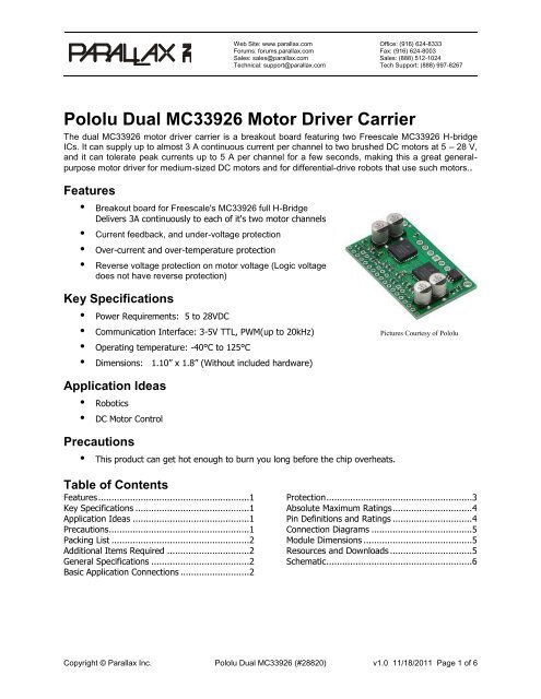
<strong>Pololu</strong> <strong>Dual</strong> <strong>MC33926</strong> <strong>Motor</strong> <strong>Driver</strong> <strong>Carrier</strong><br />
The dual <strong>MC33926</strong> motor driver carrier is a breakout board featuring two Freescale <strong>MC33926</strong> H-bridge<br />
ICs. It can supply up to almost 3 A continuous current per channel to two brushed DC motors at 5 – 28 V,<br />
and it can tolerate peak currents up to 5 A per channel for a few seconds, making this a great generalpurpose<br />
motor driver for medium-sized DC motors and for differential-drive robots that use such motors..<br />
Features<br />
• Breakout board for Freescale's <strong>MC33926</strong> full H-Bridge<br />
Delivers 3A continuously to each of it's two motor channels<br />
• Current feedback, and under-voltage protection<br />
• Over-current and over-temperature protection<br />
• Reverse voltage protection on motor voltage (Logic voltage<br />
does not have reverse protection)<br />
Key Specifications<br />
• Power Requirements: 5 to 28VDC<br />
• Communication Interface: 3-5V TTL, PWM(up to 20kHz)<br />
• Operating temperature: -40°C to 125°C<br />
• Dimensions: 1.10” x 1.8” (Without included hardware)<br />
Pictures Courtesy of <strong>Pololu</strong><br />
Application Ideas<br />
• Robotics<br />
• DC <strong>Motor</strong> Control<br />
Precautions<br />
• This product can get hot enough to burn you long before the chip overheats.<br />
Table of Contents<br />
Features ......................................................... 1<br />
Key Specifications ........................................... 1<br />
Application Ideas ............................................ 1<br />
Precautions ..................................................... 1<br />
Packing List .................................................... 2<br />
Additional Items Required ............................... 2<br />
General Specifications ..................................... 2<br />
Basic Application Connections .......................... 2<br />
Protection ....................................................... 3<br />
Absolute Maximum Ratings .............................. 4<br />
Pin Definitions and Ratings .............................. 4<br />
Connection Diagrams ...................................... 5<br />
Module Dimensions ......................................... 5<br />
Resources and Downloads ............................... 5<br />
Schematic ....................................................... 6<br />
Copyright © <strong>Parallax</strong> <strong>Inc</strong>. <strong>Pololu</strong> <strong>Dual</strong> <strong>MC33926</strong> (#28820) v1.0 11/18/2011 Page 1 of 6
Packing List<br />
• (1) <strong>MC33926</strong> <strong>Dual</strong> <strong>Carrier</strong> Board<br />
• 25-pin Straight Breakaway male Header<br />
• (3) 2-pin 3.5mm Terminal Blocks<br />
Additional Items Required<br />
• Soldering Iron and solder<br />
• Safety glasses<br />
• Heat sink (optional)<br />
General Specifications<br />
<strong>Motor</strong> <strong>Driver</strong>:<br />
<strong>Motor</strong> Channels: 2<br />
Minimum Operating Voltage:<br />
Maximum Operating Voltage:<br />
<strong>MC33926</strong><br />
5V<br />
28V<br />
Continuous Output Current per Channel: 2.5A<br />
Current Sense:<br />
Maximum PWM Frequency:<br />
0.525V/A<br />
20 kHz<br />
Minimum Logic Voltage: 2.5V<br />
Maximum Logic Voltage: 5.5V<br />
Reverse Voltage Protection?:<br />
Notes:<br />
1) Operation from 5-8V reduces maximum current output.<br />
2) The device is protected from transients up to 40V.<br />
3) The Continuous output current can be improved with the addition of a heat sink.<br />
4) SLEW pin should be HIGH for frequencies above 10kHz.<br />
5) Voltage protection is on <strong>Motor</strong> Voltage only, Logic Voltage does not have reverse protection.<br />
YES<br />
Basic Application Connections<br />
In a typical application, five I/O lines are used to connect each motor driver channel to a microcontroller:<br />
the two input lines, IN1 and IN2, for direction control, one of the disable lines, D1 or D2, for PWM speed<br />
control, the current sense output, FB, for monitoring motor current draw (connected to an analog-to-digital<br />
converter input) and the status flag, SF, for monitoring motor driver errors. The control lines can be<br />
reduced to two pins per channel if PWM signals are applied directly to the two input pins with both disable<br />
pins held inactive. In each of these cases, the other unused lines must be set to enable proper operation.<br />
Copyright © <strong>Parallax</strong> <strong>Inc</strong>. <strong>Pololu</strong> <strong>Dual</strong> <strong>MC33926</strong> (#28820) v1.0 11/18/2011 Page 2 of 6
For example, if D2 is used for the PWM input (as is typically the case), D1 must be held low to prevent it<br />
from disabling the motor driver. The circuit board provides convenient jumper points for overriding the<br />
motor driver defaults without having to connect extra wires to the module. The current sense and status<br />
flag connections are optional, though monitoring of the status flags can allow detection of latched fault<br />
conditions. The status flags are open-drain output, so the two status flag can be wired together for<br />
applications where I/O pins are scarce and determining which motor driver is experiencing a fault<br />
condition is not necessary. Note that the default state of the enable pin, EN, is LOW, which holds both<br />
motor driver chips in a low-current sleep mode. You will need to hold this pin high (either with an external<br />
connection or via the default-overriding jumper next to the pin) to allow the board to run.<br />
Protection<br />
The <strong>MC33926</strong> has under-voltage, over-current, and over-temperature protection. Some protection events<br />
are indicated by the status flag pins (SF).which are active-low pins that can be connected connected to a<br />
single input. If the chip detects an over-current or over-temperature event, the SF is latched LOW and<br />
OUT1 and OUT2 are set to high-impedance. To unlatch the status flag pin toggle the D1, D2 , EN or VIN<br />
lines. The carrier board has a reverse-protection MOSFET for added protection to the motor driver chips.<br />
Real-World Power Dissipation Considerations<br />
The <strong>MC33926</strong> motor driver used on this carrier board has a maximum current rating of 5 A continuous.<br />
However, the chip by itself will overheat at lower currents. For example, in our tests at room temperature<br />
with no forced air flow, the chip was able to deliver 5 A for 5 s and 4 A for 18 s before the chip’s thermal<br />
protection started reducing the current. A continuous current of 3 A was right at the over-temperature<br />
threshold; in some tests the thermal protection kicked in after a minute, and in other tests the chip<br />
delivered 3 A for over five minutes without triggering thermal protection. The actual current you can<br />
deliver will depend on how well you can keep the motor driver cool. The carrier’s printed circuit board is<br />
designed to draw heat out of the motor driver chips, but performance can be improved by adding a heat<br />
sink. Our tests were conducted at 100% duty cycle; PWMing the motor will introduce additional heating<br />
proportional to the frequency.<br />
Unlike other H-Bridges, the 33926 has a feature that allows it to gracefully reduce current as the<br />
current exceeds 5 A or as the chip temperature approaches its limit. This means that if you push the chip<br />
close to its limit, you will see less power to the motor, but it might allow you to avoid a complete<br />
shutdown.<br />
Copyright © <strong>Parallax</strong> <strong>Inc</strong>. <strong>Pololu</strong> <strong>Dual</strong> <strong>MC33926</strong> (#28820) v1.0 11/18/2011 Page 3 of 6
Absolute Maximum Ratings<br />
Symbol Quantity Maximum Units<br />
Vcc Supply Voltage † 28 V<br />
Pin Definitions and Ratings<br />
Pin<br />
Default Function<br />
VIN HIGH Main 5-28V motor power supply connection<br />
GND LOW Ground connection for logic and motor power supplies<br />
OUT2 HIGH The motor output pin controlled by IN2<br />
OUT1 HIGH The motor output pin controlled by IN1<br />
VDD<br />
IN2<br />
IN1<br />
PWM / D2<br />
PWM / D1<br />
SF<br />
FB<br />
HIGH<br />
HIGH<br />
HIGH<br />
LOW<br />
HIGH<br />
HIGH<br />
LOW<br />
3-5 V logic supply connection. This pin is used only for the SF pull-up and defaultoverriding<br />
jumpers; in the rare case where none of those features is used, VDD<br />
can be left disconnected<br />
The logic input control of OUT2. PWM can be applied to this pin (typically done<br />
with both disable lines inactive)<br />
The logic input control of OUT1. PWM can be applied to this pin (typically done<br />
with both disable pins inactive)<br />
Disable input: when D1 is high, OUT1 and OUT2 are set to high impedance. A D1<br />
PWM duty cycle of 70% gives a motor duty cycle of 30%. Typically, only one of<br />
the two disable pins is used, but the default is for both disable pins to be active.<br />
Disable input: when D1 is high, OUT1 and OUT2 are set to high impedance. A D1<br />
PWM duty cycle of 70% gives a motor duty cycle of 30%. Typically, only one of<br />
the two disable pins is used, but the default is for both disable pins to be active.<br />
Status flag output: an over-current (short circuit) or over-temperature event will<br />
cause SF to be latched LOW. If either of the disable pins (D1 or D2) are disabling<br />
the outputs, SF will also be LOW. Otherwise, this pin is weakly pulled high. This<br />
allows the two SF pins on the board to be tied together and connected to a single<br />
MCU input.<br />
The FB output provides analog current-sense feedback of approximately 525 mV<br />
per amp.<br />
EN LOW Enable input: when EN is LOW, both motor ICs are in a low-current sleep mode.<br />
SLEW<br />
LOW<br />
Output slew rate selection input. A logical LOW results in a slow output rise time<br />
(1.5 μs – 6 μs). A logical HIGH selects a fast output rise time (0.2 μs – 1.45 μs).<br />
This pin should be set HIGH for high-frequency (over 10 kHz) PWM. This pin<br />
determines the slew rate mode for both motor driver ICs.<br />
INV LOW A logical high value inverts the meaning of IN1 and IN2 for both motor drivers.<br />
Copyright © <strong>Parallax</strong> <strong>Inc</strong>. <strong>Pololu</strong> <strong>Dual</strong> <strong>MC33926</strong> (#28820) v1.0 11/18/2011 Page 4 of 6
Connection Diagrams<br />
Module Dimensions<br />
Size: 1.10” x 1.8” (without included hardware)<br />
Weight: 0.25 oz<br />
Resources and Downloads<br />
Check for the latest version of this document, free software from the <strong>Pololu</strong> <strong>Dual</strong> <strong>MC33926</strong> <strong>Motor</strong> <strong>Driver</strong><br />
<strong>Carrier</strong> product page. Go to www.parallax.com and search 28820.<br />
Copyright © <strong>Parallax</strong> <strong>Inc</strong>. <strong>Pololu</strong> <strong>Dual</strong> <strong>MC33926</strong> (#28820) v1.0 11/18/2011 Page 5 of 6
Schematic<br />
Copyright © <strong>Parallax</strong> <strong>Inc</strong>. <strong>Pololu</strong> <strong>Dual</strong> <strong>MC33926</strong> (#28820) v1.0 11/18/2011 Page 6 of 6