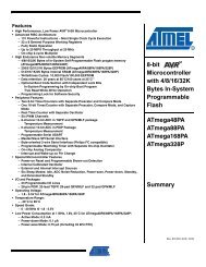
Pololu Dual MC33926 Motor Driver Carrier - Parallax, Inc.
Pololu Dual MC33926 Motor Driver Carrier - Parallax, Inc.
Pololu Dual MC33926 Motor Driver Carrier - Parallax, Inc.

You also want an ePaper? Increase the reach of your titles
YUMPU automatically turns print PDFs into web optimized ePapers that Google loves.
Absolute Maximum Ratings<br />
Symbol Quantity Maximum Units<br />
Vcc Supply Voltage † 28 V<br />
Pin Definitions and Ratings<br />
Pin<br />
Default Function<br />
VIN HIGH Main 5-28V motor power supply connection<br />
GND LOW Ground connection for logic and motor power supplies<br />
OUT2 HIGH The motor output pin controlled by IN2<br />
OUT1 HIGH The motor output pin controlled by IN1<br />
VDD<br />
IN2<br />
IN1<br />
PWM / D2<br />
PWM / D1<br />
SF<br />
FB<br />
HIGH<br />
HIGH<br />
HIGH<br />
LOW<br />
HIGH<br />
HIGH<br />
LOW<br />
3-5 V logic supply connection. This pin is used only for the SF pull-up and defaultoverriding<br />
jumpers; in the rare case where none of those features is used, VDD<br />
can be left disconnected<br />
The logic input control of OUT2. PWM can be applied to this pin (typically done<br />
with both disable lines inactive)<br />
The logic input control of OUT1. PWM can be applied to this pin (typically done<br />
with both disable pins inactive)<br />
Disable input: when D1 is high, OUT1 and OUT2 are set to high impedance. A D1<br />
PWM duty cycle of 70% gives a motor duty cycle of 30%. Typically, only one of<br />
the two disable pins is used, but the default is for both disable pins to be active.<br />
Disable input: when D1 is high, OUT1 and OUT2 are set to high impedance. A D1<br />
PWM duty cycle of 70% gives a motor duty cycle of 30%. Typically, only one of<br />
the two disable pins is used, but the default is for both disable pins to be active.<br />
Status flag output: an over-current (short circuit) or over-temperature event will<br />
cause SF to be latched LOW. If either of the disable pins (D1 or D2) are disabling<br />
the outputs, SF will also be LOW. Otherwise, this pin is weakly pulled high. This<br />
allows the two SF pins on the board to be tied together and connected to a single<br />
MCU input.<br />
The FB output provides analog current-sense feedback of approximately 525 mV<br />
per amp.<br />
EN LOW Enable input: when EN is LOW, both motor ICs are in a low-current sleep mode.<br />
SLEW<br />
LOW<br />
Output slew rate selection input. A logical LOW results in a slow output rise time<br />
(1.5 μs – 6 μs). A logical HIGH selects a fast output rise time (0.2 μs – 1.45 μs).<br />
This pin should be set HIGH for high-frequency (over 10 kHz) PWM. This pin<br />
determines the slew rate mode for both motor driver ICs.<br />
INV LOW A logical high value inverts the meaning of IN1 and IN2 for both motor drivers.<br />
Copyright © <strong>Parallax</strong> <strong>Inc</strong>. <strong>Pololu</strong> <strong>Dual</strong> <strong>MC33926</strong> (#28820) v1.0 11/18/2011 Page 4 of 6