

Circuit-Based Characterization of Device Noise Using ... - IEEE Xplore
Circuit-Based Characterization of Device Noise Using ... - IEEE Xplore
Circuit-Based Characterization of Device Noise Using ... - IEEE Xplore

You also want an ePaper? Increase the reach of your titles
YUMPU automatically turns print PDFs into web optimized ePapers that Google loves.
1266 <strong>IEEE</strong> TRANSACTIONS ON CIRCUITS AND SYSTEMS—I: REGULAR PAPERS, VOL. 57, NO. 6, JUNE 2010<br />
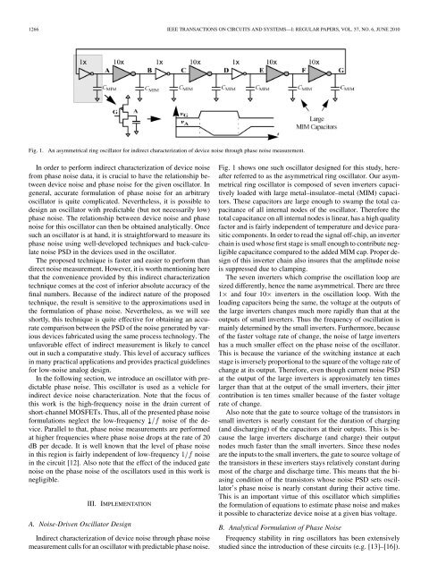
Fig. 1. An asymmetrical ring oscillator for indirect characterization <strong>of</strong> device noise through phase noise measurement.<br />
In order to perform indirect characterization <strong>of</strong> device noise<br />
from phase noise data, it is crucial to have the relationship between<br />
device noise and phase noise for the given oscillator. In<br />
general, accurate formulation <strong>of</strong> phase noise for an arbitrary<br />
oscillator is quite complicated. Nevertheless, it is possible to<br />
design an oscillator with predictable (but not necessarily low)<br />
phase noise. The relationship between device noise and phase<br />
noise for this oscillator can then be obtained analytically. Once<br />
such an oscillator is at hand, it is straightforward to measure its<br />
phase noise using well-developed techniques and back-calculate<br />
noise PSD in the devices used in the oscillator.<br />
The proposed technique is faster and easier to perform than<br />
direct noise measurement. However, it is worth mentioning here<br />
that the convenience provided by this indirect characterization<br />
technique comes at the cost <strong>of</strong> inferior absolute accuracy <strong>of</strong> the<br />
final numbers. Because <strong>of</strong> the indirect nature <strong>of</strong> the proposed<br />
technique, the result is sensitive to the approximations used in<br />
the formulation <strong>of</strong> phase noise. Nevertheless, as we will see<br />
shortly, this technique is quite effective for obtaining an accurate<br />
comparison between the PSD <strong>of</strong> the noise generated by various<br />
devices fabricated using the same process technology. The<br />
unfavorable effect <strong>of</strong> indirect measurement is likely to cancel<br />
out in such a comparative study. This level <strong>of</strong> accuracy suffices<br />
in many practical applications and provides practical guidelines<br />
for low-noise analog design.<br />
In the following section, we introduce an oscillator with predictable<br />
phase noise. This oscillator is used as a vehicle for<br />
indirect device noise characterization. Note that the focus <strong>of</strong><br />
this work is the high-frequency noise in the drain current <strong>of</strong><br />
short-channel MOSFETs. Thus, all <strong>of</strong> the presented phase noise<br />
formulations neglect the low-frequency noise <strong>of</strong> the device.<br />
Parallel to that, phase noise measurements are performed<br />
at higher frequencies where phase noise drops at the rate <strong>of</strong> 20<br />
dB per decade. It is well known that the level <strong>of</strong> phase noise<br />
in this region is fairly independent <strong>of</strong> low-frequency noise<br />
in the circuit [12]. Also note that the effect <strong>of</strong> the induced gate<br />
noise on the phase noise <strong>of</strong> the oscillators used in this work is<br />
negligible.<br />
III. IMPLEMENTATION<br />
A. <strong>Noise</strong>-Driven Oscillator Design<br />
Indirect characterization <strong>of</strong> device noise through phase noise<br />
measurement calls for an oscillator with predictable phase noise.<br />
Fig. 1 shows one such oscillator designed for this study, hereafter<br />
referred to as the asymmetrical ring oscillator. Our asymmetrical<br />
ring oscillator is composed <strong>of</strong> seven inverters capacitively<br />
loaded with large metal–insulator–metal (MIM) capacitors.<br />
These capacitors are large enough to swamp the total capacitance<br />
<strong>of</strong> all internal nodes <strong>of</strong> the oscillator. Therefore the<br />
total capacitance on all internal nodes is linear, has a high quality<br />
factor and is fairly independent <strong>of</strong> temperature and device parasitic<br />
components. In order to read the signal <strong>of</strong>f-chip, an inverter<br />
chain is used whose first stage is small enough to contribute negligible<br />
capacitance compared to the added MIM cap. Proper design<br />
<strong>of</strong> this inverter chain also insures that the amplitude noise<br />
is suppressed due to clamping.<br />
The seven inverters which comprise the oscillation loop are<br />
sized differently, hence the name asymmetrical. There are three<br />
1 and four 10 inverters in the oscillation loop. With the<br />
loading capacitors being the same, the voltage at the outputs <strong>of</strong><br />
the large inverters changes much more rapidly than that at the<br />
outputs <strong>of</strong> small inverters. Thus the frequency <strong>of</strong> oscillation is<br />
mainly determined by the small inverters. Furthermore, because<br />
<strong>of</strong> the faster voltage rate <strong>of</strong> change, the noise <strong>of</strong> large inverters<br />
has a much smaller effect on the phase noise <strong>of</strong> the oscillator.<br />
This is because the variance <strong>of</strong> the switching instance at each<br />
stage is inversely proportional to the square <strong>of</strong> the voltage rate <strong>of</strong><br />
change at its output. Therefore, even though current noise PSD<br />
at the output <strong>of</strong> the large inverters is approximately ten times<br />
larger than that at the output <strong>of</strong> the small inverters, their jitter<br />
contribution is ten times smaller because <strong>of</strong> the faster voltage<br />
rate <strong>of</strong> change.<br />
Also note that the gate to source voltage <strong>of</strong> the transistors in<br />
small inverters is nearly constant for the duration <strong>of</strong> charging<br />
(and discharging) <strong>of</strong> the capacitors at their outputs. This is because<br />
the large inverters discharge (and charge) their output<br />
nodes much faster than the small inverters. Since these nodes<br />
are the inputs to the small inverters, the gate to source voltage <strong>of</strong><br />
the transistors in these inverters stays relatively constant during<br />
most <strong>of</strong> the charge and discharge time. This means that the biasing<br />
condition <strong>of</strong> the transistors whose noise PSD sets oscillator’s<br />
phase noise is nearly constant during their active time.<br />
This is an important virtue <strong>of</strong> this oscillator which simplifies<br />
the formulation <strong>of</strong> equations to estimate phase noise and makes<br />
it possible to characterize device noise at a given bias voltage.<br />
B. Analytical Formulation <strong>of</strong> Phase <strong>Noise</strong><br />
Frequency stability in ring oscillators has been extensively<br />
studied since the introduction <strong>of</strong> these circuits (e.g. [13]–[16]).


