

Circuit-Based Characterization of Device Noise Using ... - IEEE Xplore
Circuit-Based Characterization of Device Noise Using ... - IEEE Xplore
Circuit-Based Characterization of Device Noise Using ... - IEEE Xplore

You also want an ePaper? Increase the reach of your titles
YUMPU automatically turns print PDFs into web optimized ePapers that Google loves.
1270 <strong>IEEE</strong> TRANSACTIONS ON CIRCUITS AND SYSTEMS—I: REGULAR PAPERS, VOL. 57, NO. 6, JUNE 2010<br />
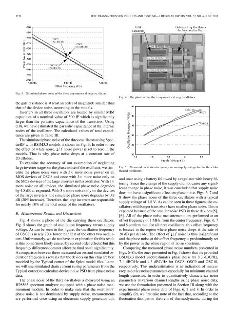
Fig. 3.<br />
Simulated phase noise <strong>of</strong> the three asymmetrical ring oscillators.<br />
the gate resistance is at least an order <strong>of</strong> magnitude smaller than<br />
that <strong>of</strong> the device noise, according to the models.<br />
Inverters in all three oscillators are loaded by similar MIM<br />
capacitors <strong>of</strong> a nominal value <strong>of</strong> 500 fF which is significantly<br />
larger than the parasitic capacitance <strong>of</strong> the transistors. <strong>Using</strong><br />
(10), we have estimated the parasitic capacitance at the internal<br />
nodes <strong>of</strong> the oscillator. The calculated values <strong>of</strong> total capacitance<br />
are given in Table III.<br />
The simulated phase noise <strong>of</strong> the three oscillators using SpectreRF<br />
with BSIM3.3 models is shown in Fig. 3. In order to see<br />
the effect <strong>of</strong> white noise, noise power is set to zero in the<br />
models. That is why phase noise drops at a constant rate <strong>of</strong><br />
20 dB/dec.<br />
To examine the accuracy <strong>of</strong> our assumption <strong>of</strong> neglecting<br />
large inverter stages on the phase noise <strong>of</strong> the oscillator, we simulate<br />
the phase noise once with 3 more noise power on all<br />
MOS devices <strong>of</strong> OSC8 and once with 3 more noise only on<br />
the MOS devices <strong>of</strong> the large inverters in this oscillator. With 3<br />
more noise on all devices, the simulated phase noise degrades<br />
by 4.8 dB as expected. With 3 more noise only on the devices<br />
<strong>of</strong> the large inverters, the simulated phase noise degrades by 0.8<br />
dB (20% increase). Therefore, the large inverters are responsible<br />
for nearly 10% <strong>of</strong> the total noise <strong>of</strong> the oscillators.<br />
B. Measurement Results and Discussions<br />
Fig. 4 shows a photo <strong>of</strong> the die carrying these oscillators.<br />
Fig. 5 shows the graph <strong>of</strong> oscillation frequency versus supply<br />
voltage. As can be seen in this figure, the oscillation frequency<br />
<strong>of</strong> OSC8 is nearly 20% lower than that <strong>of</strong> the other two oscillators.<br />
Unfortunately, we do not have an explanation for this result<br />
at this point (most likely caused by second order effects) but this<br />
frequency difference does not affect the final result significantly.<br />
A comparison between these measured curves and simulated oscillation<br />
frequencies reveals that the devices on this chip are best<br />
modeled by the Typical corner <strong>of</strong> the Spice model files. Later,<br />
we will use simulated drain current (using parameters from the<br />
Typical corner) to calculate device noise PSD from phase noise<br />
data.<br />
The phase noise <strong>of</strong> the three oscillators is measured using an<br />
HP8563 spectrum analyzer equipped with a phase noise measurement<br />
module. In order to make sure that the oscillators’<br />
phase noise is not dominated by supply noise, measurements<br />
are performed once using an electronic supply generator unit<br />
Fig. 4.<br />
Die photo <strong>of</strong> the three asymmetrical ring oscillators.<br />
Fig. 5. Measured oscillation frequency versus supply voltage for the three fabricated<br />
oscillators.<br />
and once using a battery followed by a regulator with heavy filtering.<br />
Since the change <strong>of</strong> the supply did not cause any significant<br />
change in phase noise, it was concluded that supply noise<br />
does not have a significant effect on phase noise. Figs. 6, 7 and<br />
8 show the phase noise <strong>of</strong> the three oscillators with a typical<br />
supply voltage <strong>of</strong> 1.8 V. As can be seen in these figures, the oscillators<br />
with longer transistors have smaller phase noise. This is<br />
expected because <strong>of</strong> the smaller noise PSD in these devices [5],<br />
[6]. All <strong>of</strong> the phase noise measurements are performed at an<br />
<strong>of</strong>fset frequency <strong>of</strong> 1 MHz from the center frequency. Figs. 6, 7<br />
and 8 confirm that, for all three oscillators, this <strong>of</strong>fset frequency<br />
is located in the region where phase noise drops at the rate <strong>of</strong><br />
20 dB per decade. The effect <strong>of</strong> noise is thus insignificant<br />
and the phase noise at this <strong>of</strong>fset frequency is predominantly set<br />
by the power in the white region <strong>of</strong> noise spectrum.<br />
Comparing the measured phase noise numbers presented in<br />
Figs. 6–8 to the ones presented in Fig. 3 shows that the provided<br />
BSIM3.3 model underestimates phase noise by 8.3 dBC/Hz,<br />
7.1 dBC/Hz and 4.3 dBC/Hz for OSC8, OSC9 and OSC10,<br />
respectively. This underestimation is an indication <strong>of</strong> inaccuracy<br />
in device noise parameters especially for minimum channel<br />
length transistor. In order to quantitatively characterize noise<br />
parameters at various channel lengths using phase noise data,<br />
we use the formulation presented in Section III along with the<br />
experimental phase noise data <strong>of</strong> Figs. 6, 7 and 8. In order to<br />
simplify (9), we first take note <strong>of</strong> the fact that, according to the<br />
fluctuation-dissipation theorem <strong>of</strong> thermodynamic, during the


