

Circuit-Based Characterization of Device Noise Using ... - IEEE Xplore
Circuit-Based Characterization of Device Noise Using ... - IEEE Xplore
Circuit-Based Characterization of Device Noise Using ... - IEEE Xplore

You also want an ePaper? Increase the reach of your titles
YUMPU automatically turns print PDFs into web optimized ePapers that Google loves.
<strong>IEEE</strong> TRANSACTIONS ON CIRCUITS AND SYSTEMS—I: REGULAR PAPERS, VOL. 57, NO. 6, JUNE 2010 1265<br />
<strong>Circuit</strong>-<strong>Based</strong> <strong>Characterization</strong> <strong>of</strong> <strong>Device</strong> <strong>Noise</strong><br />
<strong>Using</strong> Phase <strong>Noise</strong> Data<br />
Reza Navid, Member, <strong>IEEE</strong>, Thomas H. Lee, Member, <strong>IEEE</strong>, and Robert W. Dutton, Life Fellow, <strong>IEEE</strong><br />
Abstract—A circuit-based device noise characterization technique<br />
is introduced which uses phase noise data to estimate the<br />
power spectral density (PSD) <strong>of</strong> high-frequency noise in MOS-<br />
FETs. To apply this technique to a typical CMOS process, an<br />
oscillator structure is introduced which provides a predictable<br />
phase noise level for a given device noise PSD. The analytical<br />
equations governing the phase noise <strong>of</strong> this oscillator are presented<br />
and subsequently verified using circuit simulations. Three<br />
oscillators, using transistors <strong>of</strong> various channel lengths, are fabricated<br />
in a commercial 0.18 m CMOS process technology to<br />
study short-channel excess noise. It is shown that, at equal current<br />
levels, the noise PSD in minimum-channel-length transistors is<br />
8.7 dB larger than that in 3 -minimum-channel-length devices.<br />
The proposed method is especially suitable for applying to a<br />
state-<strong>of</strong>-the-art CMOS process to provide a quantitative analysis<br />
<strong>of</strong> various noise trade<strong>of</strong>fs which are sometimes missing in<br />
foundry-provided models.<br />
Index Terms—<strong>Device</strong> characterization, excess noise, integrated<br />
oscillator, jitter, MOSFET, noise, phase noise, ring oscillator, shortchannel<br />
effects.<br />
I. INTRODUCTION<br />
UNDERSTANDING noise in electronics is an important<br />
problem for integrated systems. The analysis <strong>of</strong> noise<br />
in these systems starts with a careful characterization <strong>of</strong> noise<br />
in the devices comprising them using physical and empirical<br />
models. Once these noise sources are sufficiently characterized,<br />
the analysis <strong>of</strong> noise at the circuit and system levels<br />
is performed using well-developed mathematical methods.<br />
Therefore, accurate characterization <strong>of</strong> device noise is arguably<br />
the most challenging task in noise analysis. These challenges<br />
have made physical modeling <strong>of</strong> device noise an active research<br />
topic for several decades since the pioneering work <strong>of</strong> J. B.<br />
Johnson [1].<br />
After the commercialization <strong>of</strong> MOSFETs in the early 1960s,<br />
extensive investigations were launched that helped designers<br />
understand major MOSFET noise sources in less than a decade.<br />
These investigations revealed that there are two partially correlated<br />
noise sources in every MOSFET: channel thermal noise<br />
[2] and induced gate noise [3]. By 1970, the classical formulation<br />
<strong>of</strong> MOSFET noise was finalized [4]. In 1986, Jindal [5]<br />
Manuscript received February 24, 2009; revised June 29, 2009; accepted<br />
August 16, 2009. First published December 28, 2009; current version published<br />
June 09, 2010. This work is supported under an SRC customized research<br />
project from Texas Instruments and MARCO MSD center. This paper was<br />
recommended by Associate Editor A. M. Klumperink.<br />
R. Navid was with Department <strong>of</strong> Electrical Engineering, Stanford University,<br />
Palo Alto, CA 94305 USA 521 Del Medio Ave., #216, Mountain View, CA<br />
94040 USA. He is now with True <strong>Circuit</strong>s Inc., Los Altos, CA 94022 USA<br />
(e-mail: rnavid@gloworm.stanford.edu).<br />
T. H. Lee and R. W. Dutton are with the Department <strong>of</strong> Electrical Engineering,<br />
Stanford University, Palo Alto, CA 94305 USA (e-mail: tomlee@ee.<br />
stanford.edu; dutton@gloworm.stanford.edu).<br />
Digital Object Identifier 10.1109/TCSI.2009.2033535<br />
and Abidi [6] suggested that the classical noise model underestimates<br />
noise power spectral density (PSD) in short-channel<br />
devices. Since then, several studies have tried to replicate those<br />
results or theoretically explain this phenomenon. These investigations<br />
have led to different (and sometimes conflicting) results<br />
for MOSFET noise behavior (see for example [7]–[9]).<br />
One <strong>of</strong> the major difficulties in the way <strong>of</strong> reaching a unified<br />
noise model for short-channel MOSFETs is experimental verification.<br />
Measuring device noise is usually a difficult process; it<br />
requires careful de-embedding <strong>of</strong> parasitic elements as well as<br />
accurate control <strong>of</strong> environmental parameters.<br />
Fortunately, direct device noise measurement is not the only<br />
way <strong>of</strong> estimating noise PSD in an electronic component.<br />
This paper introduces a circuit-based technique for MOSFET<br />
noise characterization based on phase noise measurement. This<br />
technique facilitates quantitative analysis <strong>of</strong> device noise trade<strong>of</strong>fs<br />
because, when proper design prevents parasitic Q-loading<br />
effects, phase noise is simpler and faster to measure than<br />
amplitude noise. The organization <strong>of</strong> this paper is as follows.<br />
Section II introduces the proposed technique and discusses<br />
its advantages and limitations. Section III covers an actual<br />
implementation by introducing an asymmetrical ring oscillator<br />
and the analytical formulation <strong>of</strong> its phase noise which are<br />
subsequently verified using circuit simulations. Section IV<br />
concludes this paper by presenting device noise data for a<br />
commercial 0.18 m CMOS process. Although some parts <strong>of</strong><br />
the work have been briefly reported in [10] and [11], our work<br />
on the analytical formulation <strong>of</strong> phase noise, simulation results<br />
and interpretation <strong>of</strong> the experimental data are presented here<br />
in greater detail.<br />
II. CIRCUIT-BASED CHARACTERIZATION OF DEVICE NOISE<br />
To circumvent the aforementioned difficulties in noise measurement,<br />
it is desirable to indirectly estimate noise PSD in electronic<br />
devices through characterization <strong>of</strong> a more readily measured<br />
physical quantity. One such quantity is the phase noise <strong>of</strong><br />
an oscillator. The measurement <strong>of</strong> phase noise <strong>of</strong> an electrical<br />
oscillator is <strong>of</strong>ten relatively easy to perform and the results are<br />
usually quite accurate. This is because the phase noise <strong>of</strong> an<br />
oscillator is mainly set by the noise sources and electrical components<br />
“inside” the oscillation loop. Thus, most <strong>of</strong>f-chip parasitic<br />
elements do not have a significant effect on the phase noise<br />
<strong>of</strong> integrated oscillators. Furthermore, phase noise measurement<br />
is a comparative measurement between the signal power at the<br />
center frequency and that at a small <strong>of</strong>fset frequency [12]. Therefore,<br />
the effects <strong>of</strong> many parasitic elements such as cable loss<br />
and impedance mismatch are significantly canceled out, greatly<br />
reducing the number <strong>of</strong> non-idealities in phase noise measurement<br />
and making it faster and less costly to perform.<br />
1549-8328/$26.00 © 2010 <strong>IEEE</strong>
1266 <strong>IEEE</strong> TRANSACTIONS ON CIRCUITS AND SYSTEMS—I: REGULAR PAPERS, VOL. 57, NO. 6, JUNE 2010<br />
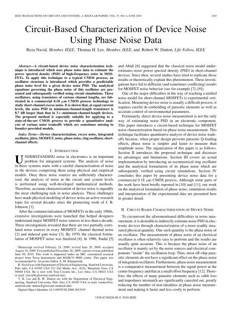
Fig. 1. An asymmetrical ring oscillator for indirect characterization <strong>of</strong> device noise through phase noise measurement.<br />
In order to perform indirect characterization <strong>of</strong> device noise<br />
from phase noise data, it is crucial to have the relationship between<br />
device noise and phase noise for the given oscillator. In<br />
general, accurate formulation <strong>of</strong> phase noise for an arbitrary<br />
oscillator is quite complicated. Nevertheless, it is possible to<br />
design an oscillator with predictable (but not necessarily low)<br />
phase noise. The relationship between device noise and phase<br />
noise for this oscillator can then be obtained analytically. Once<br />
such an oscillator is at hand, it is straightforward to measure its<br />
phase noise using well-developed techniques and back-calculate<br />
noise PSD in the devices used in the oscillator.<br />
The proposed technique is faster and easier to perform than<br />
direct noise measurement. However, it is worth mentioning here<br />
that the convenience provided by this indirect characterization<br />
technique comes at the cost <strong>of</strong> inferior absolute accuracy <strong>of</strong> the<br />
final numbers. Because <strong>of</strong> the indirect nature <strong>of</strong> the proposed<br />
technique, the result is sensitive to the approximations used in<br />
the formulation <strong>of</strong> phase noise. Nevertheless, as we will see<br />
shortly, this technique is quite effective for obtaining an accurate<br />
comparison between the PSD <strong>of</strong> the noise generated by various<br />
devices fabricated using the same process technology. The<br />
unfavorable effect <strong>of</strong> indirect measurement is likely to cancel<br />
out in such a comparative study. This level <strong>of</strong> accuracy suffices<br />
in many practical applications and provides practical guidelines<br />
for low-noise analog design.<br />
In the following section, we introduce an oscillator with predictable<br />
phase noise. This oscillator is used as a vehicle for<br />
indirect device noise characterization. Note that the focus <strong>of</strong><br />
this work is the high-frequency noise in the drain current <strong>of</strong><br />
short-channel MOSFETs. Thus, all <strong>of</strong> the presented phase noise<br />
formulations neglect the low-frequency noise <strong>of</strong> the device.<br />
Parallel to that, phase noise measurements are performed<br />
at higher frequencies where phase noise drops at the rate <strong>of</strong> 20<br />
dB per decade. It is well known that the level <strong>of</strong> phase noise<br />
in this region is fairly independent <strong>of</strong> low-frequency noise<br />
in the circuit [12]. Also note that the effect <strong>of</strong> the induced gate<br />
noise on the phase noise <strong>of</strong> the oscillators used in this work is<br />
negligible.<br />
III. IMPLEMENTATION<br />
A. <strong>Noise</strong>-Driven Oscillator Design<br />
Indirect characterization <strong>of</strong> device noise through phase noise<br />
measurement calls for an oscillator with predictable phase noise.<br />
Fig. 1 shows one such oscillator designed for this study, hereafter<br />
referred to as the asymmetrical ring oscillator. Our asymmetrical<br />
ring oscillator is composed <strong>of</strong> seven inverters capacitively<br />
loaded with large metal–insulator–metal (MIM) capacitors.<br />
These capacitors are large enough to swamp the total capacitance<br />
<strong>of</strong> all internal nodes <strong>of</strong> the oscillator. Therefore the<br />
total capacitance on all internal nodes is linear, has a high quality<br />
factor and is fairly independent <strong>of</strong> temperature and device parasitic<br />
components. In order to read the signal <strong>of</strong>f-chip, an inverter<br />
chain is used whose first stage is small enough to contribute negligible<br />
capacitance compared to the added MIM cap. Proper design<br />
<strong>of</strong> this inverter chain also insures that the amplitude noise<br />
is suppressed due to clamping.<br />
The seven inverters which comprise the oscillation loop are<br />
sized differently, hence the name asymmetrical. There are three<br />
1 and four 10 inverters in the oscillation loop. With the<br />
loading capacitors being the same, the voltage at the outputs <strong>of</strong><br />
the large inverters changes much more rapidly than that at the<br />
outputs <strong>of</strong> small inverters. Thus the frequency <strong>of</strong> oscillation is<br />
mainly determined by the small inverters. Furthermore, because<br />
<strong>of</strong> the faster voltage rate <strong>of</strong> change, the noise <strong>of</strong> large inverters<br />
has a much smaller effect on the phase noise <strong>of</strong> the oscillator.<br />
This is because the variance <strong>of</strong> the switching instance at each<br />
stage is inversely proportional to the square <strong>of</strong> the voltage rate <strong>of</strong><br />
change at its output. Therefore, even though current noise PSD<br />
at the output <strong>of</strong> the large inverters is approximately ten times<br />
larger than that at the output <strong>of</strong> the small inverters, their jitter<br />
contribution is ten times smaller because <strong>of</strong> the faster voltage<br />
rate <strong>of</strong> change.<br />
Also note that the gate to source voltage <strong>of</strong> the transistors in<br />
small inverters is nearly constant for the duration <strong>of</strong> charging<br />
(and discharging) <strong>of</strong> the capacitors at their outputs. This is because<br />
the large inverters discharge (and charge) their output<br />
nodes much faster than the small inverters. Since these nodes<br />
are the inputs to the small inverters, the gate to source voltage <strong>of</strong><br />
the transistors in these inverters stays relatively constant during<br />
most <strong>of</strong> the charge and discharge time. This means that the biasing<br />
condition <strong>of</strong> the transistors whose noise PSD sets oscillator’s<br />
phase noise is nearly constant during their active time.<br />
This is an important virtue <strong>of</strong> this oscillator which simplifies<br />
the formulation <strong>of</strong> equations to estimate phase noise and makes<br />
it possible to characterize device noise at a given bias voltage.<br />
B. Analytical Formulation <strong>of</strong> Phase <strong>Noise</strong><br />
Frequency stability in ring oscillators has been extensively<br />
studied since the introduction <strong>of</strong> these circuits (e.g. [13]–[16]).
NAVID et al.: CIRCUIT-BASED CHARACTERIZATION OF DEVICE NOISE USING PHASE NOISE DATA 1267<br />
Fig. 2. Simplified model <strong>of</strong> the oscillator <strong>of</strong> Fig. 1 suitable for phase noise analysis. The length <strong>of</strong> T<br />
is exaggerated for better readability.<br />
In this work, we use a method that is tailored for the oscillator <strong>of</strong><br />
Fig. 1. To calculate the phase noise <strong>of</strong> this oscillator, we model<br />
it as a switching-based oscillator in which the energy injecting<br />
elements have a countable number <strong>of</strong> states and the transitions<br />
between these states can be considered instantaneous. Since the<br />
10 stages are significantly faster than 1 stages, we neglect<br />
their effect on the oscillation frequency and phase noise. Fig. 2<br />
shows a simplified model for the oscillator. As required by the<br />
switching-based oscillator model, each <strong>of</strong> the small inverters is<br />
assumed to have only three distinct states: charging, discharging<br />
and equilibrium. In its charging state , the PMOS transistor<br />
is assumed to deliver a constant current <strong>of</strong> . In this<br />
state, the inverter’s output resistance and noise PSD are<br />
and , respectively. In its discharging state , the NMOS<br />
transistor is assumed to sink a constant current <strong>of</strong> . In this<br />
state, the inverters’s output resistance and noise PSD are<br />
and , respectively. During charging and discharging states,<br />
the inverter’s current, output resistance and noise PSD are assumed<br />
to be independent <strong>of</strong> the output voltage. 1 In its equilibrium<br />
state , one <strong>of</strong> the devices in the inverter is in equilibrium<br />
while the other device is turned <strong>of</strong>f. In this state, the inverter<br />
can be replaced by a noisy resistor. 2 The moment at which<br />
an inverter moves from one state to another is referred to as a<br />
switching instance.<br />
To calculate phase noise, we use the approach presented in<br />
[11]: first we calculate jitter in the time domain and then convert<br />
that to the frequency domain to find phase noise. To calculate<br />
jitter, we first calculate the variance <strong>of</strong> each switching instance.<br />
We then add up the variances <strong>of</strong> all switching instances in one<br />
period <strong>of</strong> oscillation (assuming probabilistic independence) to<br />
find the total variance <strong>of</strong> the duration <strong>of</strong> one period, hereafter referred<br />
to as the period jitter. In order to calculate the variance <strong>of</strong><br />
a switching instance, we first find the variance <strong>of</strong> the respective<br />
control voltage at the nominal switching moment and then divide<br />
that by the square <strong>of</strong> the voltage rate <strong>of</strong> change on that node.<br />
1 These assumptions are best satisfied during the first half <strong>of</strong> T and T .<br />
These regions are indeed where we use these assumptions.<br />
2 The word “equilibrium” is used according to its thermodynamical definition.<br />
<strong>Based</strong> on this definition, a MOSFET is in equilibrium when v = v =<br />
I =0. There are, in fact, two distinguishable equilibrium states for the inverter:<br />
one in which the NMOS transistor conducts and one in which the PMOS<br />
transistor conducts. This fact has been taken into account in the presented formulation.<br />
The rest <strong>of</strong> this subsection presents the mathematical derivations<br />
<strong>of</strong> phase noise using this approach.<br />
There are six switching instances in each period <strong>of</strong> oscillation.<br />
In order to calculate the variance <strong>of</strong> the switching instance<br />
, we first need to calculate the variance <strong>of</strong> at that time. It<br />
can be shown that the variance <strong>of</strong> the voltage across a capacitor<br />
( for brevity) connected in parallel with a resistor<br />
and a current noise source with a PSD <strong>of</strong> after time is given<br />
by [11]<br />
where is the variance <strong>of</strong> at time , is Boltzmann<br />
constant and is the absolute temperature. To calculate the variance<br />
<strong>of</strong> at , we can break the time interval between and<br />
into three regions: the second half <strong>of</strong> (charging state),<br />
(equilibrium state) and the first half <strong>of</strong> (discharging<br />
state). We can then replace the inverter with its simplified model<br />
in each <strong>of</strong> these regions, assume<br />
, and use (1) consecutively<br />
to calculate at .<br />
Fortunately, certain approximations can be used to simplify<br />
this analysis. Namely, during the equilibrium time the circuit’s<br />
time constant is which is a small number<br />
since the PMOS device is in linear region. According to (1), if<br />
the equilibrium time is much longer than the circuit time<br />
constant in this region (a condition which is usually satisfied),<br />
at the end <strong>of</strong> this time interval is independent <strong>of</strong> its variance<br />
at the end <strong>of</strong> and is given by<br />
where and are the noise PSD and output conductance<br />
<strong>of</strong> the PMOS transistor during .<br />
Other approximations are possible during the first half <strong>of</strong><br />
. In this region, the output impedance <strong>of</strong> the inverter is<br />
which is normally a large number (the NMOS device<br />
is in saturation region). Assuming that is much smaller<br />
than during this time, we can replace the exponential<br />
(1)<br />
(2)
1268 <strong>IEEE</strong> TRANSACTIONS ON CIRCUITS AND SYSTEMS—I: REGULAR PAPERS, VOL. 57, NO. 6, JUNE 2010<br />
TABLE I<br />
DESIGN PARAMETERS FOR THE SEVEN ASYMMETRICAL RING OSCILLATORS USED FOR SIMULATION-BASED VERIFICATION OF THE ACCURACY OF THE PHASE<br />
NOISE PRESENTED FORMULATION<br />
terms in (1) with their series expansion. The variance <strong>of</strong><br />
is then given by<br />
at<br />
Finally, phase noise at an <strong>of</strong>fset frequency <strong>of</strong><br />
is large enough to ignore the contribution <strong>of</strong><br />
phase noise) is given by [17]<br />
(assuming<br />
noise on<br />
(3)<br />
where we have used , and<br />
in (1). In (3), is the noise PSD <strong>of</strong> the NMOS<br />
transistor during the first half <strong>of</strong> . To further simplify (3),<br />
note that can be written as<br />
where is the oscillation period and and are<br />
the dc currents <strong>of</strong> PMOS and NMOS during charging and discharging<br />
the load capacitor , respectively. <strong>Using</strong> (4) in<br />
(3) we get<br />
To find the variance <strong>of</strong> the switching instance at , we divide<br />
by the square <strong>of</strong> the voltage rate <strong>of</strong> change which is<br />
to get<br />
Similarly, the variance <strong>of</strong> the switching instance at<br />
given by<br />
To find period jitter, we note that there are three independent<br />
switching jitters <strong>of</strong> the type <strong>of</strong> and three independent<br />
switching jitters <strong>of</strong> the type <strong>of</strong> in each period <strong>of</strong> oscillation.<br />
Thus the total period jitter is<br />
(4)<br />
(5)<br />
(6)<br />
is<br />
(7)<br />
(8)<br />
The foregoing analysis uses several simplifying assumptions<br />
about the behavior <strong>of</strong> 1 inverter stages. Namely, the interstage<br />
noise effects are neglected. That is, variations <strong>of</strong> the voltage<br />
on node A do not affect the voltage on node B regardless <strong>of</strong><br />
the inverter’s state. Furthermore, first crossing approximation is<br />
used which assumes that each stage switches to a new state as<br />
soon as its input reaches a certain switching level for the first<br />
time [18]. For simplicity we also assumed that each inverter<br />
switches its state when its input voltage reaches . This can<br />
be achieved by proper sizing <strong>of</strong> NMOS and PMOS transistors.<br />
The validity <strong>of</strong> these simplifying assumptions and the accuracy<br />
<strong>of</strong> the presented formulation is verified in the following section<br />
using circuit phase noise simulations.<br />
C. Verification <strong>of</strong> the Model<br />
Seven asymmetrical ring oscillators <strong>of</strong> the type shown in<br />
Fig. 1 are designed to verify the accuracy <strong>of</strong> the presented formulation<br />
using SpectreRF phase noise simulations. The design<br />
parameters are shown in Table I. Seven different fabrication<br />
process models at 0.25 m, 0.18 m and 0.13 m technology<br />
nodes are utilized.<br />
All inverters in all three oscillators are loaded by an ideal capacitor<br />
<strong>of</strong><br />
which is significantly larger than the<br />
parasitic capacitance <strong>of</strong> the transistors. Thus the loading capacitance<br />
is, to the first order, the same in these oscillators. <strong>Using</strong> circuit<br />
simulation, we have estimated the parasitic capacitance at<br />
internal nodes by increasing the loading capacitance to<br />
and taking note <strong>of</strong> the frequency change. The effective value<br />
<strong>of</strong> the parasitic capacitance can be found using the following<br />
equation:<br />
(9)<br />
(10)
NAVID et al.: CIRCUIT-BASED CHARACTERIZATION OF DEVICE NOISE USING PHASE NOISE DATA 1269<br />
TABLE II<br />
DEVICE PARAMETERS AND PHASE NOISE NUMBERS FOR THE SEVEN ASYMMETRICAL RING OSCILLATORS. PHASE NOISE IS GIVEN AT 1 MHz OFFSET FREQUENCY<br />
AT T=60 C<br />
TABLE III<br />
DESIGN PARAMETERS FOR THREE FABRICATED ASYMMETRICAL RING OSCILLATORS<br />
where and are the oscillation frequencies before<br />
and after increasing the loading capacitance, respectively.<br />
The calculated value <strong>of</strong> total capacitance is 525 fF for TSMC<br />
0.18- m process (OSC1). The same number is used for the other<br />
oscillators as the variation is small.<br />
In order to calculate phase noise using the presented formulation,<br />
several device parameters are needed. Table II shows some<br />
<strong>of</strong> the simulated device parameters for the devices used in these<br />
oscillators. BSIM3 models are used with HSPICE simulator and<br />
is set to 1.3 V, 1.8 V and 2.5 V for 0.13 m, 0.18 m and<br />
0.25 m processes respectively. 3 Table II also shows the calculated<br />
phase noise obtained by using these device parameters in<br />
(9) as well as the simulated phase noise using SpectreRF. 4 In<br />
order to see the effect <strong>of</strong> white noise, the noise power is set<br />
to zero in the models. As can be seen in this table, phase noise<br />
numbers calculated using (9) are within 1 dB <strong>of</strong> the numbers<br />
3 Model parameters for these processes are obtained from MOSIS web site<br />
(publicly available). Due to a nondisclosure agreement with the foundry, we<br />
cannot present numerical values <strong>of</strong> the device parameters for the fabricated oscillators.<br />
4 Phase noise is calculated based on the definition <strong>of</strong> power spectral density<br />
<strong>of</strong> the signal divided by the power <strong>of</strong> the first harmonic. The simulated signal<br />
level at the first harmonic is around 1 dBV, 02 dBV and 05 dBV for the 0.25<br />
, 0.18 and 0.13 oscillators, respectively. The difference is mainly due to<br />
the difference in supply voltage.<br />
obtained from SpectreRF phase noise simulations. This level <strong>of</strong><br />
accuracy corresponds to 1 dB accuracy in device noise power. 5<br />
IV. EXPERIMENTAL RESULTS AND DISCUSSION<br />
A. Oscillator Design<br />
Three asymmetrical ring oscillators <strong>of</strong> the type shown in<br />
Fig. 1 are fabricated in a 0.18- m CMOS process and used to<br />
extract MOSFET noise parameters from experimental phase<br />
noise data. In order to highlight excess noise in short-channel<br />
devices, these oscillators use transistors with various channel<br />
lengths. The sizings <strong>of</strong> transistors are shown in Table III. The<br />
width-to-length ratio has been kept constant to ensure comparable<br />
oscillation frequencies. This helps to cancel out the effect<br />
<strong>of</strong> the approximations used in our phase noise formulation<br />
when the final device noise numbers are compared to each<br />
other. The transistors are built with multiple gate fingers to<br />
minimize gate resistance noise. In all cases, the noise PSD <strong>of</strong><br />
5 The numbers in Table II are based on models that do not take into account<br />
excess noise in short-channel devices. Thus the difference between the simulated<br />
phase noise <strong>of</strong> these oscillators can be explained based on their power<br />
consumption. Similarly, the calculated phase noise numbers are based on transistor<br />
current noise power obtained from the same models and follow the same<br />
trend. This does not affect the purpose <strong>of</strong> Table II which is to validate (9).
1270 <strong>IEEE</strong> TRANSACTIONS ON CIRCUITS AND SYSTEMS—I: REGULAR PAPERS, VOL. 57, NO. 6, JUNE 2010<br />
Fig. 3.<br />
Simulated phase noise <strong>of</strong> the three asymmetrical ring oscillators.<br />
the gate resistance is at least an order <strong>of</strong> magnitude smaller than<br />
that <strong>of</strong> the device noise, according to the models.<br />
Inverters in all three oscillators are loaded by similar MIM<br />
capacitors <strong>of</strong> a nominal value <strong>of</strong> 500 fF which is significantly<br />
larger than the parasitic capacitance <strong>of</strong> the transistors. <strong>Using</strong><br />
(10), we have estimated the parasitic capacitance at the internal<br />
nodes <strong>of</strong> the oscillator. The calculated values <strong>of</strong> total capacitance<br />
are given in Table III.<br />
The simulated phase noise <strong>of</strong> the three oscillators using SpectreRF<br />
with BSIM3.3 models is shown in Fig. 3. In order to see<br />
the effect <strong>of</strong> white noise, noise power is set to zero in the<br />
models. That is why phase noise drops at a constant rate <strong>of</strong><br />
20 dB/dec.<br />
To examine the accuracy <strong>of</strong> our assumption <strong>of</strong> neglecting<br />
large inverter stages on the phase noise <strong>of</strong> the oscillator, we simulate<br />
the phase noise once with 3 more noise power on all<br />
MOS devices <strong>of</strong> OSC8 and once with 3 more noise only on<br />
the MOS devices <strong>of</strong> the large inverters in this oscillator. With 3<br />
more noise on all devices, the simulated phase noise degrades<br />
by 4.8 dB as expected. With 3 more noise only on the devices<br />
<strong>of</strong> the large inverters, the simulated phase noise degrades by 0.8<br />
dB (20% increase). Therefore, the large inverters are responsible<br />
for nearly 10% <strong>of</strong> the total noise <strong>of</strong> the oscillators.<br />
B. Measurement Results and Discussions<br />
Fig. 4 shows a photo <strong>of</strong> the die carrying these oscillators.<br />
Fig. 5 shows the graph <strong>of</strong> oscillation frequency versus supply<br />
voltage. As can be seen in this figure, the oscillation frequency<br />
<strong>of</strong> OSC8 is nearly 20% lower than that <strong>of</strong> the other two oscillators.<br />
Unfortunately, we do not have an explanation for this result<br />
at this point (most likely caused by second order effects) but this<br />
frequency difference does not affect the final result significantly.<br />
A comparison between these measured curves and simulated oscillation<br />
frequencies reveals that the devices on this chip are best<br />
modeled by the Typical corner <strong>of</strong> the Spice model files. Later,<br />
we will use simulated drain current (using parameters from the<br />
Typical corner) to calculate device noise PSD from phase noise<br />
data.<br />
The phase noise <strong>of</strong> the three oscillators is measured using an<br />
HP8563 spectrum analyzer equipped with a phase noise measurement<br />
module. In order to make sure that the oscillators’<br />
phase noise is not dominated by supply noise, measurements<br />
are performed once using an electronic supply generator unit<br />
Fig. 4.<br />
Die photo <strong>of</strong> the three asymmetrical ring oscillators.<br />
Fig. 5. Measured oscillation frequency versus supply voltage for the three fabricated<br />
oscillators.<br />
and once using a battery followed by a regulator with heavy filtering.<br />
Since the change <strong>of</strong> the supply did not cause any significant<br />
change in phase noise, it was concluded that supply noise<br />
does not have a significant effect on phase noise. Figs. 6, 7 and<br />
8 show the phase noise <strong>of</strong> the three oscillators with a typical<br />
supply voltage <strong>of</strong> 1.8 V. As can be seen in these figures, the oscillators<br />
with longer transistors have smaller phase noise. This is<br />
expected because <strong>of</strong> the smaller noise PSD in these devices [5],<br />
[6]. All <strong>of</strong> the phase noise measurements are performed at an<br />
<strong>of</strong>fset frequency <strong>of</strong> 1 MHz from the center frequency. Figs. 6, 7<br />
and 8 confirm that, for all three oscillators, this <strong>of</strong>fset frequency<br />
is located in the region where phase noise drops at the rate <strong>of</strong><br />
20 dB per decade. The effect <strong>of</strong> noise is thus insignificant<br />
and the phase noise at this <strong>of</strong>fset frequency is predominantly set<br />
by the power in the white region <strong>of</strong> noise spectrum.<br />
Comparing the measured phase noise numbers presented in<br />
Figs. 6–8 to the ones presented in Fig. 3 shows that the provided<br />
BSIM3.3 model underestimates phase noise by 8.3 dBC/Hz,<br />
7.1 dBC/Hz and 4.3 dBC/Hz for OSC8, OSC9 and OSC10,<br />
respectively. This underestimation is an indication <strong>of</strong> inaccuracy<br />
in device noise parameters especially for minimum channel<br />
length transistor. In order to quantitatively characterize noise<br />
parameters at various channel lengths using phase noise data,<br />
we use the formulation presented in Section III along with the<br />
experimental phase noise data <strong>of</strong> Figs. 6, 7 and 8. In order to<br />
simplify (9), we first take note <strong>of</strong> the fact that, according to the<br />
fluctuation-dissipation theorem <strong>of</strong> thermodynamic, during the
NAVID et al.: CIRCUIT-BASED CHARACTERIZATION OF DEVICE NOISE USING PHASE NOISE DATA 1271<br />
which after solving for<br />
gives<br />
(12)<br />
Fig. 6. Phase noise <strong>of</strong> OSC8 (L =0:18 m) at v =1:8 V.<br />
Fig. 7. Phase noise graph for OSC9 (L =0:38 m) at v =1:8 V.<br />
Fig. 8. Phase noise graph for OSC10 (L =0:54 ) at v =1:8 V.<br />
equilibrium time , the noise PSD in the NMOS and PMOS<br />
devices are given by and , respectively. If we<br />
further assume that the current flow in NMOS and PMOS transistors<br />
are nearly equal and equal to ( through<br />
proper device sizing), (9) can be simplified to<br />
(11)<br />
In order to find the total noise PSD<br />
we use<br />
(12) along with the value <strong>of</strong> from simulation results<br />
(Spice models at Typical corner) and the values <strong>of</strong> and<br />
from the measurements. For a supply voltage <strong>of</strong> 1.8<br />
V , in this 0.18 CMOS process, total drain<br />
current noise PSD (NMOS+PMOS) is ,<br />
, and at 0.18 , 0.38 ,<br />
and 0.54 channel length, respectively. Note that although<br />
the absolute accuracy <strong>of</strong> these numbers is affected by several<br />
sources <strong>of</strong> error inherent to our indirect noise measurement<br />
approach, the relative accuracy can be used with a higher<br />
confidence. This is because, most <strong>of</strong> these errors are common<br />
between the three oscillators and hence they cancel out when<br />
the numbers are compared to each other.<br />
Although the presented experiment provides the total drain<br />
current noise PSD (NMOS+PMOS), it also possible to individually<br />
calculate the noise <strong>of</strong> NMOS and PMOS devices through<br />
a similar experiment. In such an experiment, one needs to build<br />
two asymmetrical oscillators <strong>of</strong> the type shown in Fig. 1 with<br />
different NMOS to PMOS ratios. It will then be possible to<br />
use (9) for the two oscillators and solve the two equations for<br />
and . Unfortunately, at the time <strong>of</strong> this submission, such<br />
structures are not available to us.<br />
According to the presented data, in this process, total noise<br />
PSD can be reduced by nearly 5.3 dB and 8.7 dB by increasing<br />
the channel length <strong>of</strong> the transistors from minimum channel<br />
length to 2 and 3 minimum channel length, respectively (at<br />
a constant width over length ratio). Measurements <strong>of</strong> the oscillation<br />
frequency (as well as simulation results) show that the<br />
total current (hence power consumption) will stay nearly constant<br />
under this transformation.<br />
In many applications, speed requirements limit the maximum<br />
channel length that can be used for a certain circuit. Nevertheless,<br />
if the speed requirement is not the limiting factor, longchannel<br />
transistors should be used as much as possible to minimize<br />
noise PSD. This recommendation is consistent with the<br />
general wisdom: For optimum noise operation, a circuit should<br />
be only as fast as needed and not any faster than that.<br />
In practice, some foundries prohibit the use <strong>of</strong> transistors<br />
with longer than minimum channel length. In some cases,<br />
the accuracy <strong>of</strong> the models is not guaranteed for devices with<br />
longer-than-minimum channel lengths and/or the matching<br />
between these devices is not as well controlled as between minimum-channel-length<br />
devices. In these cases, potential circuit<br />
impairments should be carefully studied before a decision is<br />
made on using long-channel devices. In some cases, the use <strong>of</strong><br />
stacked devices, as a way to emulate longer transistors, can be<br />
an attractive alternative.<br />
V. CONCLUSIONS<br />
A circuit-based method is introduced for indirect characterization<br />
<strong>of</strong> device noise using phase noise data. Compared to<br />
amplitude noise, phase noise is <strong>of</strong>ten easier to measure and<br />
less sensitive to measurement non-idealities and environmental<br />
conditions. We presented an asymmetrical oscillator with
1272 <strong>IEEE</strong> TRANSACTIONS ON CIRCUITS AND SYSTEMS—I: REGULAR PAPERS, VOL. 57, NO. 6, JUNE 2010<br />
predictable phase noise to back-calculate the noise PSD <strong>of</strong><br />
MOSFETs from measured phase noise data. The analytical<br />
formulation <strong>of</strong> phase noise for this oscillator is presented and<br />
subsequently verified using circuit simulations. <strong>Using</strong> this<br />
oscillator, drain noise PSD in transistors <strong>of</strong> various channel<br />
lengths fabricated in a commercial 0.18 CMOS process is<br />
estimated from measured phase noise data. According to this<br />
data, the drain current noise can be reduced by nearly 8.7 dB<br />
by using 3 minimum channel length device instead <strong>of</strong> minimum-channel-length<br />
device if permitted by speed requirement<br />
and foundry rules. The introduced method can be used for<br />
in-house noise characterization <strong>of</strong> state-<strong>of</strong>-the-art devices when<br />
foundry models lack reliable noise data.<br />
ACKNOWLEDGMENT<br />
The authors would like to thank S. S. Mohan <strong>of</strong> Magma Design<br />
Automation for enlightening discussions.<br />
REFERENCES<br />
[1] J. B. Johnson, “Thermal agitation <strong>of</strong> electricity in conductors,” Phys.<br />
Rev., vol. 119, pp. 97–109, July 1927.<br />
[2] A. G. Jordan and N. A. Jordan, “Theory <strong>of</strong> noise in metal oxide semiconductor<br />
devices,” <strong>IEEE</strong> Trans. Electron <strong>Device</strong>s, vol. ED-12, no. 5,<br />
pp. 148–156, Mar. 1965.<br />
[3] M. Shonji, “Analysis <strong>of</strong> high frequency thermal noise <strong>of</strong> enhancement<br />
mode MOS field-effect transistors,” <strong>IEEE</strong> Trans. Electron <strong>Device</strong>s, vol.<br />
ED-13, no. 6, pp. 520–524, Jun. 1966.<br />
[4] Y. P. Tsividis, Operation and Modeling <strong>of</strong> the MOS Transistor. New<br />
York: Wiley, 1987.<br />
[5] R. P. Jindal, “Hot-electron effects on channel thermal noise in fineline<br />
NMOS field-effect transistors,” <strong>IEEE</strong> Trans. Electron <strong>Device</strong>s, vol.<br />
ED-33, no. 9, pp. 1395–1397, Sep. 1986.<br />
[6] A. A. Abidi, “High-frequency noise measurements on FET’s with<br />
small dimensions,” <strong>IEEE</strong> Trans. Electron <strong>Device</strong>s, vol. ED-33, no. 11,<br />
pp. 1801–1805, Nov. 1986.<br />
[7] D. P. Triantis, A. N. Birbas, and D. Kondis, “Thermal noise modeling<br />
for short-channel MOSFETs,” <strong>IEEE</strong> Trans. Electron <strong>Device</strong>s, vol.<br />
ED-43, no. 11, pp. 1950–1955, Nov. 1996.<br />
[8] G. Knoblinger, P. Klein, and M. Tiebout, “A new model for thermal<br />
channel noise <strong>of</strong> deep submicron MOSFETs and its application in<br />
RF-CMOS design,” <strong>IEEE</strong> J. Solid-State <strong>Circuit</strong>s, vol. SSC-36, no. 5,<br />
pp. 831–837, May 2001.<br />
[9] A. J. Scholten, L. F. Tiemeijer, R. van Langevelde, R. J. Havens, A. T.<br />
A. Zegers-van Duijnhoven, and V. C. Venezia, “<strong>Noise</strong> modeling for RF<br />
CMOS circuit simulation,” <strong>IEEE</strong> Trans. Electron <strong>Device</strong>s, vol. ED-50,<br />
no. 3, pp. 618–632, Mar. 2003.<br />
[10] R. Navid, T. H. Lee, and R. W. Dutton, “A circuit-based noise parameter<br />
extraction technique for MOSFETs,” in <strong>IEEE</strong> Int. Symp. on <strong>Circuit</strong>s<br />
Syst. (ISCAS) Dig. Tech. Papers, May 2007, pp. 3347–3350.<br />
[11] R. Navid, T. H. Lee, and R. W. Dutton, “Minimum achievable phase<br />
noise <strong>of</strong> RC oscillators,” <strong>IEEE</strong> J. Solid-State <strong>Circuit</strong>s, vol. SC-40, no.<br />
3, pp. 630–637, Mar. 2005.<br />
[12] T. H. Lee, The Design <strong>of</strong> CMOS Radio-Frequency Integrated <strong>Circuit</strong>s.<br />
Cambridge, U.K.: Cambridge Univ. Press, 1998.<br />
[13] J. A. McNeill, “Jitter in ring oscillators,” <strong>IEEE</strong> J. Solid-State <strong>Circuit</strong>s,<br />
vol. SC-32, no. 6, pp. 870–879, Jun. 1997.<br />
[14] B. H. Leung and D. Mcleish, “Investigation <strong>of</strong> phase noise <strong>of</strong> ring oscillators<br />
with time-varying current and noise sources by time-scaling<br />
thermal noise,” <strong>IEEE</strong> Trans. <strong>Circuit</strong>s Syst. I, Reg. Papers, vol. 51, no.<br />
10, pp. 1926–1939, Oct. 2004.<br />
[15] A. A. Abidi, “Phase noise and jitter in CMOS ring oscillators,” <strong>IEEE</strong><br />
J. Solid-State <strong>Circuit</strong>s, vol. SC-41, pp. 1803–1816, Aug. 2006.<br />
[16] S. Srivastava and J. Roychowdhury, “Analytical equations for nonlinear<br />
phase errors and jitter in ring oscillator,” <strong>IEEE</strong> Trans. <strong>Circuit</strong>s Syst. I,<br />
Reg. Papers, vol. 54, no. 10, pp. 2321–2329, Oct. 2007.<br />
[17] L. E. Larson, RF and Microwave <strong>Circuit</strong> Design for Wireless Communications.<br />
Norwood, MA: Artech House, 1996.<br />
[18] A. A. Abidi and R. G. Meyer, “<strong>Noise</strong> in relaxation oscillators,” <strong>IEEE</strong><br />
J. Solid-State <strong>Circuit</strong>s, vol. SC-18, no. 6, pp. 794–802, Dec. 1988.<br />
Reza Navid (M’05) received the B.S. degree from<br />
the University <strong>of</strong> Tehran, Tehran, Iran, the M.S. degree<br />
from Sharif University <strong>of</strong> Technology, Tehran,<br />
Iran, and the Ph.D. degree from Stanford University,<br />
Stanford, CA, in 1996, 1998, and 2005, respectively,<br />
all in electrical engineering.<br />
From 1998 to 2000, he was with ParsElectric MFG<br />
Corporation, Tehran, Iran, where he worked on RF<br />
circuits for TV tuners. From January 2000 to May<br />
2001 he was with the University <strong>of</strong> Michigan, Ann<br />
Arbor, as a researcher working on MEMS for wireless<br />
communications. He spent the summer <strong>of</strong> 2001 with Maxim Integrated<br />
Products, Hillsboro, OR, where he worked on a 3.125-Gbit/s high-speed communication<br />
receiver front-end. From 2005 to 2008 he was with Rambus Inc.,<br />
Los Altos, CA, working on high-speed integrated circuits for chip-to-chip and<br />
memory link applications. He is now with True <strong>Circuit</strong>s Inc., Los Altos, California.<br />
His current research interests include low-phase-noise timing circuits for<br />
various communication and data conversion systems.<br />
Thomas H. Lee (S’87–M’88) received the S.B., S.M.<br />
and Sc.D. degrees from the Massachusetts Institute <strong>of</strong><br />
Technology in 1983, 1985, and 1990, respectively, all<br />
in electrical engineering.<br />
He joined Analog <strong>Device</strong>s in 1990 where he was<br />
primarily engaged in the design <strong>of</strong> high-speed clock<br />
recovery devices. In 1992, he joined Rambus Inc.,<br />
Mountain View, CA where he developed high-speed<br />
analog circuitry for 500 megabyte/s CMOS DRAMs.<br />
He has also contributed to the development <strong>of</strong> PLLs<br />
in the StrongARM, Alpha and AMD K6/K7/K8 microprocessors.<br />
Since 1994, he has been a Pr<strong>of</strong>essor <strong>of</strong> Electrical Engineering<br />
at Stanford University where his research focus has been on gigahertz-speed<br />
wireline and wireless integrated circuits built in conventional silicon technologies,<br />
particularly CMOS. He holds 43 U.S. patents and authored The Design<br />
<strong>of</strong> CMOS Radio-Frequency Integrated <strong>Circuit</strong>s (now in its second edition), and<br />
Planar Microwave Engineering, both with Cambridge University Press. He is a<br />
co-author <strong>of</strong> four additional books on RF circuit design, and also c<strong>of</strong>ounded Matrix<br />
Semiconductor (acquired by Sandisk in 2006). He is the founder <strong>of</strong> ZeroG<br />
Wireless.<br />
Dr. Lee has twice received the “Best Paper” award at the International Solid-<br />
State <strong>Circuit</strong>s Conference, co-authored a “Best Student Paper” at ISSCC, was<br />
awarded the Best Paper prize at CICC, and is a Packard Foundation Fellowship<br />
recipient. He is an <strong>IEEE</strong> Distinguished Lecturer <strong>of</strong> the Solid-State <strong>Circuit</strong>s Society,<br />
and has been a DL <strong>of</strong> the <strong>IEEE</strong> Microwave Society as well.<br />
Robert W. Dutton (S’67–M’70–SM’80–F’84–LF’10)<br />
received the B.S., M.S., and Ph.D. degrees from the<br />
University <strong>of</strong> California, Berkeley, in 1966, 1967, and<br />
1970, respectively.<br />
He is Pr<strong>of</strong>essor <strong>of</strong> Electrical Engineering at<br />
Stanford University and director <strong>of</strong> Integrated<br />
<strong>Circuit</strong>s Laboratory. He has held summer staff<br />
positions at Fairchild, Bell Telephone Laboratories,<br />
Hewlett-Packard, IBM Research, and Matsushita<br />
during 1967, 1973, 1975, 1977, and 1988 respectively.<br />
His research interests focus on Integrated<br />
<strong>Circuit</strong> process, device, and circuit technologies—especially the use <strong>of</strong> Computer-Aided<br />
Design (CAD) in device scaling and for RF applications. He has<br />
published more than 200 journal articles and graduated more than four dozen<br />
doctorate students.<br />
Dr. Dutton was Editor <strong>of</strong> the <strong>IEEE</strong> TRANSACTIONS ON COMPUTER-AIDED<br />
DESIGN OF INTERGATED CIRCUITS AND SYSTEMS (1984–1986), winner <strong>of</strong> the<br />
1987 <strong>IEEE</strong> J. J. Ebers, and 1996 Jack Morton Awards, 1988 Guggenheim Fellowship<br />
to study in Japan, was elected to the National Academy <strong>of</strong> Engineering<br />
in 1991, honored with the C&C Prize (Japan) in 2000, received Career Achievement<br />
Award (2005) from the Semiconductor Industry Association (SIA) for sustained<br />
contributions in support <strong>of</strong> research that is critical to SIA needs, and the<br />
Phil Kaufman Award in 2006.


