

Circuit-Based Characterization of Device Noise Using ... - IEEE Xplore
Circuit-Based Characterization of Device Noise Using ... - IEEE Xplore
Circuit-Based Characterization of Device Noise Using ... - IEEE Xplore

Create successful ePaper yourself
Turn your PDF publications into a flip-book with our unique Google optimized e-Paper software.
1268 <strong>IEEE</strong> TRANSACTIONS ON CIRCUITS AND SYSTEMS—I: REGULAR PAPERS, VOL. 57, NO. 6, JUNE 2010<br />
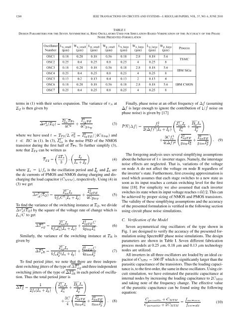
TABLE I<br />
DESIGN PARAMETERS FOR THE SEVEN ASYMMETRICAL RING OSCILLATORS USED FOR SIMULATION-BASED VERIFICATION OF THE ACCURACY OF THE PHASE<br />
NOISE PRESENTED FORMULATION<br />
terms in (1) with their series expansion. The variance <strong>of</strong><br />
is then given by<br />
at<br />
Finally, phase noise at an <strong>of</strong>fset frequency <strong>of</strong><br />
is large enough to ignore the contribution <strong>of</strong><br />
phase noise) is given by [17]<br />
(assuming<br />
noise on<br />
(3)<br />
where we have used , and<br />
in (1). In (3), is the noise PSD <strong>of</strong> the NMOS<br />
transistor during the first half <strong>of</strong> . To further simplify (3),<br />
note that can be written as<br />
where is the oscillation period and and are<br />
the dc currents <strong>of</strong> PMOS and NMOS during charging and discharging<br />
the load capacitor , respectively. <strong>Using</strong> (4) in<br />
(3) we get<br />
To find the variance <strong>of</strong> the switching instance at , we divide<br />
by the square <strong>of</strong> the voltage rate <strong>of</strong> change which is<br />
to get<br />
Similarly, the variance <strong>of</strong> the switching instance at<br />
given by<br />
To find period jitter, we note that there are three independent<br />
switching jitters <strong>of</strong> the type <strong>of</strong> and three independent<br />
switching jitters <strong>of</strong> the type <strong>of</strong> in each period <strong>of</strong> oscillation.<br />
Thus the total period jitter is<br />
(4)<br />
(5)<br />
(6)<br />
is<br />
(7)<br />
(8)<br />
The foregoing analysis uses several simplifying assumptions<br />
about the behavior <strong>of</strong> 1 inverter stages. Namely, the interstage<br />
noise effects are neglected. That is, variations <strong>of</strong> the voltage<br />
on node A do not affect the voltage on node B regardless <strong>of</strong><br />
the inverter’s state. Furthermore, first crossing approximation is<br />
used which assumes that each stage switches to a new state as<br />
soon as its input reaches a certain switching level for the first<br />
time [18]. For simplicity we also assumed that each inverter<br />
switches its state when its input voltage reaches . This can<br />
be achieved by proper sizing <strong>of</strong> NMOS and PMOS transistors.<br />
The validity <strong>of</strong> these simplifying assumptions and the accuracy<br />
<strong>of</strong> the presented formulation is verified in the following section<br />
using circuit phase noise simulations.<br />
C. Verification <strong>of</strong> the Model<br />
Seven asymmetrical ring oscillators <strong>of</strong> the type shown in<br />
Fig. 1 are designed to verify the accuracy <strong>of</strong> the presented formulation<br />
using SpectreRF phase noise simulations. The design<br />
parameters are shown in Table I. Seven different fabrication<br />
process models at 0.25 m, 0.18 m and 0.13 m technology<br />
nodes are utilized.<br />
All inverters in all three oscillators are loaded by an ideal capacitor<br />
<strong>of</strong><br />
which is significantly larger than the<br />
parasitic capacitance <strong>of</strong> the transistors. Thus the loading capacitance<br />
is, to the first order, the same in these oscillators. <strong>Using</strong> circuit<br />
simulation, we have estimated the parasitic capacitance at<br />
internal nodes by increasing the loading capacitance to<br />
and taking note <strong>of</strong> the frequency change. The effective value<br />
<strong>of</strong> the parasitic capacitance can be found using the following<br />
equation:<br />
(9)<br />
(10)


