

Surface and bulk passivation of multicrystalline silicon solar cells by ...
Surface and bulk passivation of multicrystalline silicon solar cells by ...
Surface and bulk passivation of multicrystalline silicon solar cells by ...

Create successful ePaper yourself
Turn your PDF publications into a flip-book with our unique Google optimized e-Paper software.
13<br />
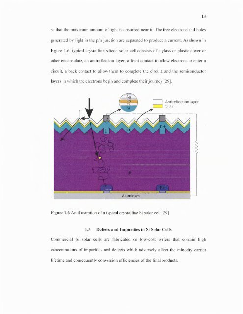
so that the maximum amount <strong>of</strong> light is absorbed near it. The free electrons <strong>and</strong> holes<br />
generated <strong>by</strong> light in the p/n junction are separated to produce a current. As shown in<br />
Figure 1.6, typical crystalline <strong>silicon</strong> <strong>solar</strong> cell consists <strong>of</strong> a glass or plastic cover or<br />
other encapsulate, an antireflection layer, a front contact to allow electrons to enter a<br />
circuit, a back contact to allow them to complete the circuit, <strong>and</strong> the semiconductor<br />
layers in which the electrons begin <strong>and</strong> complete their journey [29].<br />
Figure 1.6 An illustration <strong>of</strong> a typical crystalline Si <strong>solar</strong> cell [29]<br />
1.5 Defects <strong>and</strong> Impurities in Si Solar Cells<br />
Commercial Si <strong>solar</strong> <strong>cells</strong> are fabricated on low-cost wafers that contain high<br />
concentrations <strong>of</strong> impurities <strong>and</strong> defects which adversely affect the minority carrier<br />
lifetime <strong>and</strong> consequently conversion efficiencies <strong>of</strong> the final products.


