Phase Control Using Thyristors - Littelfuse
Phase Control Using Thyristors - Littelfuse
Phase Control Using Thyristors - Littelfuse

You also want an ePaper? Increase the reach of your titles
YUMPU automatically turns print PDFs into web optimized ePapers that Google loves.
AN10039<br />
<strong>Phase</strong> <strong>Control</strong> <strong>Using</strong> <strong>Thyristors</strong><br />
Introduction<br />
Due to high-volume production techniques, thyristors are now<br />
priced so that almost any electrical product can benefit from electronic<br />
control. A look at the fundamentals of SCR and triac phase<br />
controls shows how this is possible.<br />
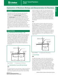
Output Power Characteristics<br />
<strong>Phase</strong> control is the most common form of thyristor power control.<br />
The thyristor is held in the off condition — that is, all current<br />
flow in the circuit is blocked by the thyristor except a minute leakage<br />
current. Then the thyristor is triggered into an “on” condition<br />
by the control circuitry.<br />
For full-wave AC control, a single triac or two SCRs connected in<br />
inverse parallel may be used. One of two methods may be used<br />
for full-wave DC control — a bridge rectifier formed by two SCRs<br />
or an SCR placed in series with a diode bridge as shown in<br />
Figure AN1003.1.<br />
It is important to note that the circuit current is determined by the<br />
load and power source. For simplification, assume the load is<br />
resistive; that is, both the voltage and current waveforms are<br />
identical.<br />
Full-wave Rectified Operation<br />
Voltage Applied to Load<br />
Delay (Triggering) Angle<br />
Conduction Angle<br />
Figure AN1003.2 Sine Wave Showing Principles of <strong>Phase</strong> <strong>Control</strong><br />
Different loads respond to different characteristics of the AC<br />
waveform. For example, some are sensitive to average voltage,<br />
some to RMS voltage, and others to peak voltage. Various voltage<br />
characteristics are plotted against conduction angle for<br />
half- and full-wave phase control circuits in Figure AN1003.3<br />
and Figure AN1003.4.<br />
Line<br />
<strong>Control</strong><br />
Circuit<br />
Load<br />
Line<br />
<strong>Control</strong><br />
Circuit<br />
Load<br />
Two SCR AC <strong>Control</strong><br />
Triac AC <strong>Control</strong><br />
Line<br />
Line<br />
<strong>Control</strong><br />
Circuit<br />
<strong>Control</strong><br />
Circuit<br />
Load<br />
Load<br />
One SCR DC <strong>Control</strong><br />
Two SCR DC <strong>Control</strong><br />
Figure AN1003.1 SCR/Triac Connections for Various Methods of<br />
<strong>Phase</strong> <strong>Control</strong><br />
Figure AN1003.2 illustrates voltage waveform and shows common<br />
terms used to describe thyristor operation. Delay angle is<br />
the time during which the thyristor blocks the line voltage. The<br />
conduction angle is the time during which the thyristor is on.<br />
©2002 Teccor Electronics AN1003 - 1 http://www.teccor.com<br />
Thyristor Product Catalog +1 972-580-7777
AN1003<br />
Application Notes<br />
Normalized Sine Wave RMS Voltage Power<br />
as Fraction of Full Conduction<br />
1.8<br />
1.6<br />
1.4<br />
1.2<br />
1.0<br />
0.8<br />
0.6<br />
0.4<br />
0.2<br />
Figure AN1003.3<br />
HALF WAVE<br />
Peak Voltage<br />
Power<br />
RMS<br />
AVG<br />
0<br />
0 20 40 60 80 100 120 140 160 180<br />
θ<br />
Conduction Angle (θ)<br />
Half-Wave <strong>Phase</strong> <strong>Control</strong> (Sinusoidal)<br />
FULL WAVE<br />
θ<br />
θ<br />
phase angle. Thus, a 180° conduction angle in a half-wave circuit<br />
provides 0.5 x full-wave conduction power.<br />
In a full-wave circuit, a conduction angle of 150° provides 97%<br />
full power while a conduction angle of 30° provides only 3% of full<br />
power control. Therefore, it is usually pointless to obtain conduction<br />
angles less than 30° or greater than 150°.<br />
Figure AN1003.5 and Figure AN1003.6 give convenient direct<br />
output voltage readings for 115 V/230 V input voltage. These<br />
curves also apply to current in a resistive circuit.<br />
Output Voltage<br />
Input<br />
Voltage<br />
230 V 115 V<br />
360 180<br />
320 160<br />
280 140<br />
240 120<br />
200 100<br />
160<br />
120<br />
80<br />
40<br />
0<br />
80<br />
60<br />
40<br />
20<br />
HALF WAVE<br />
RMS<br />
θ<br />
Peak Voltage<br />
0 0 20 40 60 80 100 120 140 160 180<br />
Conduction Angle (θ)<br />
AVG<br />
1.8<br />
Figure AN1003.5<br />
Output Voltage of Half-wave <strong>Phase</strong><br />
Normal Sine Wave RMS Voltage Power<br />
as Fraction of Full Conduction<br />
1.6<br />
1.4<br />
1.2<br />
1.0<br />
0.8<br />
0.6<br />
0.4<br />
0.2<br />
Figure AN1003.4<br />
Peak Voltage<br />
Power<br />
RMS<br />
0<br />
0 20 40 60 80 100 120 140 160 180<br />
Conduction Angle (θ)<br />
Symmetrical Full-Wave <strong>Phase</strong> <strong>Control</strong> (Sinusoidal)<br />
Figure AN1003.3 and Figure AN1003.4 also show the relative<br />
power curve for constant impedance loads such as heaters.<br />
Because the relative impedance of incandescent lamps and<br />
motors change with applied voltage, they do not follow this curve<br />
precisely. To use the curves, find the full-wave rated power of the<br />
load, and then multiply by the ratio associated with the specific<br />
AVG<br />
Output Voltage<br />
Input<br />
Voltage<br />
230 V 115 V<br />
360 180<br />
320 160<br />
280 140<br />
240 120<br />
200 100<br />
160<br />
120<br />
80<br />
40<br />
0<br />
Figure AN1003.6<br />
80<br />
60<br />
40<br />
20<br />
FULL WAVE<br />
RMS<br />
θ<br />
Peak Voltage<br />
0<br />
0 20 40 60 80 100 120 140 160 180<br />
Conduction Angle (θ)<br />
AVG<br />
Output Voltage of Full-wave <strong>Phase</strong> <strong>Control</strong><br />
θ<br />
http://www.teccor.com AN1003 - 2 ©2002 Teccor Electronics<br />
+1 972-580-7777 Thyristor Product Catalog
Application Notes<br />
AN1003<br />
<strong>Control</strong> Characteristics<br />
A relaxation oscillator is the simplest and most common control<br />
circuit for phase control. Figure AN1003.7 illustrates this circuit<br />
as it would be used with a thyristor. Turn-on of the thyristor<br />
occurs when the capacitor is charged through the resistor from a<br />
voltage or current source until the breakover voltage of the<br />
switching device is reached. Then, the switching device changes<br />
to its on state, and the capacitor is discharged through the thyristor<br />
gate. Trigger devices used are neon bulbs, unijunction transistors,<br />
and three-, four-, or five-layer semiconductor trigger<br />
devices. <strong>Phase</strong> control of the output waveform is obtained by<br />
varying the RC time constant of the charging circuit so the trigger<br />
device breakdown occurs at different phase angles within the<br />
controlled half or full cycle.<br />
Voltage<br />
or<br />
Current<br />
Source<br />
R<br />
Figure AN1003.7<br />
C<br />
Switching<br />
Device<br />
Relaxation Oscillator Thyristor Trigger Circuit<br />
Figure AN1003.8 shows the capacitor voltage-time characteristic<br />
if the relaxation oscillator is to be operated from a pure DC<br />
source.<br />
Capacitor Voltage<br />
Supply Source Voltage )<br />
Ratio of (<br />
1.0<br />
0.9<br />
0.8<br />
0.7<br />
0.6<br />
0.5<br />
0.4<br />
0.3<br />
0.2<br />
0.1<br />
Figure AN1003.8 Capacitor Charging from DC Source<br />
Usually, the design starting point is the selection of a capacitance<br />
value which will reliably trigger the thyristor when the capacitance<br />
is discharged. Trigger devices and thyristor gate triggering characteristics<br />
play a part in the selection. All the device characteristics<br />
are not always completely specified in applications, so<br />
experimental determination is sometimes needed.<br />
SCR<br />
0<br />
0 1 2 3 4 5 6<br />
Time Constants<br />
Triac<br />
Upon final selection of the capacitor, the curve shown in Figure<br />
AN1003.8 can be used in determining the charging resistance<br />
needed to obtain the desired control characteristics.<br />
Many circuits begin each half-cycle with the capacitor voltage at<br />
or near zero. However, most circuits leave a relatively large<br />
residual voltage on the capacitor after discharge. Therefore, the<br />
charging resistor must be determined on the basis of additional<br />
charge necessary to raise the capacitor to trigger potential.<br />
For example, assume that we want to trigger an S2010L SCR<br />
with a 32 V trigger diac. A 0.1 µF capacitor will supply the necessary<br />
SCR gate current with the trigger diac. Assume a 50 V dc<br />
power supply, 30° minimum conduction angle, and 150° maximum<br />
conduction angle with a 60 Hz input power source. At<br />
approximately 32 V, the diac triggers leaving 0.66 V BO of diac<br />
voltage on the capacitor. In order for diac to trigger, 22 V must be<br />
added to the capacitor potential, and 40 V additional (50-10) are<br />
available. The capacitor must be charged to 22/40 or 0.55 of the<br />
available charging voltage in the desired time. Looking at Figure<br />
AN1003.8, 0.55 of charging voltage represents 0.8 time constant.<br />
The 30° conduction angle required that the firing pulse be<br />
delayed 150° or 6.92 ms. (The period of 1/2 cycle at 60 Hz is<br />
8.33 ms.) To obtain this time delay:<br />
6.92 ms = 0.8 RC<br />
RC = 8.68 ms<br />
if C = 0.10 µF<br />
–3<br />
8.6810<br />
then, R = ------------------------- =<br />
–6<br />
86,000 <br />
0.110<br />
To obtain the minimum R (150° conduction angle), the delay is<br />
30° or<br />
(30/180) x 8.33 = 1.39 ms<br />
1.39 ms = 0.8 RC<br />
RC = 1.74 ms<br />
–3<br />
1.7410<br />
R = -------------------------- =<br />
–6<br />
17,400 <br />
0.110<br />
<strong>Using</strong> practical values, a 100 k potentiometer with up to 17 k minimum<br />
(residual) resistance should be used. Similar calculations<br />
using conduction angles between the maximum and minimum<br />
values will give control resistance versus power characteristic of<br />
this circuit.<br />
Triac <strong>Phase</strong> <strong>Control</strong><br />
The basic full-wave triac phase control circuit shown in<br />
Figure AN1003.9 requires only four components. Adjustable<br />
resistor R 1 and C 1 are a single-element phase-shift network.<br />
When the voltage across C 1 reaches breakover voltage (V BO ) of<br />
the diac, C 1 is partially discharged by the diac into the triac gate.<br />
The triac is then triggered into the conduction mode for the<br />
remainder of that half-cycle. In this circuit, triggering is in Quadrants<br />
I and III. The unique simplicity of this circuit makes it suitable<br />
for applications with small control range.<br />
©2002 Teccor Electronics AN1003 - 3 http://www.teccor.com<br />
Thyristor Product Catalog +1 972-580-7777
AN1003<br />
Application Notes<br />
Load<br />
Triac<br />
R 1 250 k (Q2010L5)<br />
100<br />
3.3 k<br />
R<br />
120 V<br />
2<br />
(60 Hz) (For Inductive<br />
Loads)<br />
C 1<br />
0.1 µF<br />
Diac<br />
HT34B<br />
0.1 µF<br />
120 V<br />
(60 Hz)<br />
Load<br />
R 2<br />
C 2<br />
0.1 µF<br />
68 k<br />
R 4<br />
R 1<br />
R 3<br />
100 k<br />
Trim<br />
C 1<br />
0.1 µF<br />
3.3 k<br />
250 k<br />
Triac<br />
(Q2010L5)<br />
Diac<br />
HT34B<br />
Figure AN1003.9<br />
Basic Diac-Triac <strong>Phase</strong> <strong>Control</strong><br />
The hysteresis (snap back) effect is somewhat similar to the<br />
action of a kerosene lantern. That is, when the control knob is<br />
first rotated from the off condition, the lamp can be lit only at<br />
some intermediate level of brightness, similar to turning up the<br />
wick to light the lantern. Brightness can then be turned down until<br />
it finally reaches the extinguishing point. If this occurs, the lamp<br />
can only be relit by turning up the control knob again to the intermediate<br />
level. Figure AN1003.10 illustrates the hysteresis effect<br />
in capacitor-diac triggering. As R 1 is brought down from its maximum<br />
resistance, the voltage across the capacitor increases until<br />
the diac first fires at point A, at the end of a half-cycle (conduction<br />
angle i). After the gate pulse, however, the capacitor voltage<br />
drops suddenly to about half the triggering voltage, giving the<br />
capacitor a different initial condition. The capacitor charges to the<br />
diac, triggering voltage at point B in the next half-cycle and giving<br />
a steady-state conduction angle shown as for the triac.<br />
Figure AN1003.11<br />
Extended Range Full-wave <strong>Phase</strong> <strong>Control</strong><br />
By using one of the circuits shown in Figure AN1003.12, the hysteresis<br />
effect can be eliminated entirely. The circuit (a) resets the<br />
timing capacitor to the same level after each positive half-cycle,<br />
providing a uniform initial condition for the timing capacitor. This<br />
circuit is useful only for resistive loads since the firing angle is not<br />
symmetrical throughout the range. If symmetrical firing is<br />
required, use the circuit (b) shown in Figure AN1003.12.<br />
(a)<br />
120 V<br />
(60 Hz)<br />
Load<br />
R 2<br />
D 2<br />
15 k<br />
1/2 W<br />
D 1<br />
R 3<br />
R 1<br />
C 1<br />
0.1 µF<br />
3.3 k<br />
250 k<br />
Triac<br />
(Q2010L5)<br />
Diac<br />
D 1 , D 2 = 200 V Diodes<br />
AC Line<br />
Diac Triggers at "A"<br />
θ<br />
[+Diac V BO]<br />
(b)<br />
Load<br />
R 2<br />
R 4<br />
R 3<br />
Triac<br />
(Q2010L5)<br />
A<br />
B<br />
[–Diac VBO]<br />
120 V<br />
(60 Hz)<br />
D 1<br />
D 3<br />
R 1<br />
D 4<br />
Capacitor<br />
Voltage<br />
Diac Does Not<br />
Trigger at "A"<br />
θ i<br />
D 2<br />
C 1<br />
0.1 µF<br />
Diac<br />
Figure AN1003.10 Relationship of AC Line Voltage and Triggering<br />
Voltage<br />
In the Figure AN1003.11 illustration, the addition of a second RC<br />
phase-shift network extends the range on control and reduces<br />
the hysteresis effect to a negligible region. This circuit will control<br />
from 5% to 95% of full load power, but is subject to supply voltage<br />
variations. When R 1 is large, C 1 is charged primarily through<br />
R 3 from the phase-shifted voltage appearing across C 2 . This<br />
action provides additional range of phase-shift across C 1 and<br />
enables C 2 to partially recharge C 1 after the diac has triggered,<br />
thus reducing hysteresis. R 3 should be adjusted so that the circuit<br />
just drops out of conduction when R 1 is brought to maximum<br />
resistance.<br />
Figure AN1003.12<br />
R 1 = 250 k POT<br />
R 2 , R 3 = 15 k, 1/2 W<br />
R 4 = 3.3 k<br />
D 1 , D 2 , D 3 , D 4 = 200 V Diodes<br />
Wide-range Hysteresis Free <strong>Phase</strong> <strong>Control</strong><br />
For more complex control functions, particularly closed loop controls,<br />
the unijunction transistor may be used for the triggering<br />
device in a ramp and pedestal type of firing circuit as shown in<br />
Figure AN1003.13.<br />
http://www.teccor.com AN1003 - 4 ©2002 Teccor Electronics<br />
+1 972-580-7777 Thyristor Product Catalog
Application Notes<br />
AN1003<br />
120 V<br />
(60 Hz)<br />
Load<br />
R1<br />
D1<br />
D3<br />
Figure AN1003.13<br />
UJT Triggering Level<br />
Pedestal<br />
UJT Emitter Voltage<br />
D2<br />
D4<br />
R2<br />
D5<br />
Cool<br />
Hot<br />
R3<br />
R5<br />
Temp<br />
R4<br />
R1, R2 = 2.2 k, 2 W<br />
R3 = 2.2 k, 1/2 W<br />
R4 = Thermistor, approx. 5 k<br />
at operating temperature<br />
R5 = 10 k Potentiometer<br />
R6 = 5 M Potentiometer<br />
R7 = 100 k, 1/2 W<br />
R8 = 1 k, 1/2 W<br />
Precision Proportional Temperature <strong>Control</strong><br />
Several speed control and light dimming (phase) control circuits<br />
have been presented that give details for a complete 120 V application<br />
circuit but none for 240 V. Figure AN1003.14 and Figure<br />
AN1003.15 show some standard phase control circuits for 240 V,<br />
60 Hz/50 Hz operation along with 120 V values for comparison.<br />
Even though there is very little difference, there are a few key<br />
things that must be remembered. First, capacitors and triacs connected<br />
across the 240 V line must be rated at 400 V. Secondly,<br />
the potentiometer (variable resistor) value must change considerably<br />
to obtain the proper timing or triggering for 180° in each halfcycle.<br />
Figure AN1003.14 shows a simple single-time-constant light dimmer<br />
(phase control) circuit, giving values for both 120 V and<br />
240 V operation.<br />
0<br />
T<br />
Ramp<br />
R6<br />
D6<br />
Time<br />
R7<br />
C1<br />
"Gain"<br />
T1<br />
Q1 = 2N2646<br />
Q2 = Q2010L5<br />
T1 = Dale PT 10-101<br />
or equivalent<br />
D1-4 = 200 V Diode<br />
D5 = 20 V Zener<br />
D6 = 100 V Diode<br />
C1 = 0.1 µF, 30 V<br />
R8<br />
Q1<br />
Q2<br />
Triac<br />
AC<br />
Input<br />
AC<br />
Input<br />
Voltage<br />
Load<br />
120 V ac<br />
60 Hz<br />
240 V ac<br />
50/60 Hz<br />
Figure AN1003.14<br />
C1<br />
12 A<br />
3 A<br />
L1<br />
R1<br />
C2<br />
Note: L1 and C1 form an<br />
RFI filter that may be eliminated<br />
AC<br />
Load<br />
Current<br />
R 1 C 1 , C 3 L 1 Q 1<br />
250 k<br />
500 k<br />
R2<br />
3.3 k<br />
0.1 µF<br />
100 V<br />
HT-32<br />
0.1 µF 200 V<br />
0.1 µF 400 V<br />
100 µH<br />
200 µH<br />
Q2015L9<br />
Q4004L4<br />
Single-time-constant Circuit for Incandescent Light<br />
Dimming, Heat <strong>Control</strong>, and Motor Speed <strong>Control</strong><br />
The circuit shown in Figure AN1003.15 is a double-time-constant<br />
circuit which has improved performance compared to the circuit<br />
shown in Figure AN1003.14. This circuit uses an additional RC<br />
network to extend the phase angle so that the triac can be triggered<br />
at small conduction angles. The additional RC network<br />
also minimizes any hysteresis effect explained and illustrated in<br />
Figure AN1003.10 and Figure AN1003.11.<br />
AC<br />
Input<br />
Load<br />
C 1<br />
D1<br />
Q1<br />
R3 *<br />
100<br />
C3 *<br />
* dv/dt snubber network<br />
when required<br />
L 1<br />
R 1<br />
3.3 k<br />
R 4 *<br />
Q<br />
100<br />
1<br />
R 3<br />
R 2 D<br />
15 k 1<br />
1/2 W<br />
C 2 C 3<br />
C<br />
HT-32<br />
4 *<br />
0.1 µF<br />
100 V<br />
Note: L 1 and C 1 form an<br />
RFI filter that may be eliminated<br />
* dv/dt snubber network<br />
when required<br />
AC<br />
Input<br />
Voltage<br />
AC<br />
Load<br />
Current<br />
R2<br />
C1, C2, C4<br />
L1<br />
Q1<br />
120 V ac<br />
60 Hz<br />
8 A<br />
250 k<br />
0.1 µF 200 V<br />
100 µH<br />
Q2010L5<br />
240 V ac<br />
50 Hz<br />
6 A<br />
500 k<br />
0.1 µF 400 V<br />
200 µH<br />
Q4008L4<br />
240 V ac<br />
60 Hz<br />
6 A<br />
500 k<br />
0.1 µF 400 V<br />
200 µH<br />
Q4008L4<br />
Figure AN1003.15<br />
Double-time-constant Circuit for Incandescent Light<br />
Dimming, Heat <strong>Control</strong>, and Motor Speed <strong>Control</strong><br />
©2002 Teccor Electronics AN1003 - 5 http://www.teccor.com<br />
Thyristor Product Catalog +1 972-580-7777
AN1003<br />
Application Notes<br />
Permanent Magnet Motor <strong>Control</strong><br />
Figure AN1003.16 illustrates a circuit for phase controlling a permanent<br />
magnet (PM) motor. Since PM motors are also generators,<br />
they have characteristics that make them difficult for a<br />
standard triac to commutate properly. <strong>Control</strong> of a PM motor is<br />
easily accomplished by using an alternistor triac with enhanced<br />
commutating characteristics.<br />
AC<br />
Input<br />
Load<br />
SCR1<br />
CR1<br />
R1<br />
R2<br />
2.2 k<br />
+<br />
R3<br />
115 V ac<br />
Input<br />
DC<br />
MTR<br />
Figure AN1003.16 Circuit for <strong>Phase</strong> <strong>Control</strong>ling a Permanent Magnet<br />
Motor<br />
PM motors normally require full-wave DC rectification. Therefore,<br />
the alternistor triac controller should be connected in series with<br />
the AC input side of the rectifier bridge. The possible alternative<br />
of putting an SCR controller in series with the motor on the DC<br />
side of the rectifier bridge can be a challenge when it comes to<br />
timing and delayed turn-on near the end of the half cycle. The<br />
alternistor triac controller shown in Figure AN1003.16 offers a<br />
wide range control so that the alternistror triac can be triggered at<br />
a small conduction angle or low motor speed; the rectifiers and<br />
alternistors should have similar voltage ratings, with all based on<br />
line voltage and actual motor load requirements.<br />
SCR <strong>Phase</strong> <strong>Control</strong><br />
-<br />
1.5 A<br />
250 k<br />
0.1 µF<br />
400 V<br />
Figure AN1003.17 shows a very simple variable resistance halfwave<br />
circuit. It provides phase retard from essentially zero (SCR<br />
full on) to 90 electrical degrees of the anode voltage wave (SCR<br />
half on). Diode CR 1 blocks reverse gate voltage on the negative<br />
half-cycle of anode supply voltage. This protects the reverse gate<br />
junction of sensitive SCRs and keeps power dissipation low for<br />
gate resistors on the negative half cycle. The diode is rated to<br />
block at least the peak value of the AC supply voltage. The retard<br />
angle cannot be extended beyond the 90-degree point because<br />
the trigger circuit supply voltage and the trigger voltage producing<br />
the gate current to fire are in phase. At the peak of the AC<br />
supply voltage, the SCR can still be triggered with the maximum<br />
value of resistance between anode and gate. Since the SCR will<br />
trigger and latch into conduction the first time I GT is reached, its<br />
conduction cannot be delayed beyond 90 electrical degrees with this<br />
circuit.<br />
3.3 k<br />
15 k 1/2 W<br />
0.1 µF<br />
100 V<br />
Q4006LH4<br />
G<br />
HT-32<br />
MT2<br />
MT1<br />
100<br />
0.1 µF<br />
400 V<br />
AC<br />
Input<br />
Voltage<br />
120 V ac<br />
60 Hz<br />
120 V ac<br />
60 Hz<br />
240 V ac<br />
60 Hz<br />
240 V ac<br />
60 Hz<br />
240 V ac<br />
50Hz<br />
Figure AN1003.17<br />
0.8 A<br />
8.5 A<br />
0.8 A<br />
8.5 A<br />
2.5 A<br />
500 k<br />
100 k<br />
1 M<br />
250 k<br />
1 M<br />
IN4003<br />
IN4003<br />
IN4004<br />
IN4004<br />
IN4004<br />
Half-wave <strong>Control</strong>, 0° to 90° Conduction<br />
Figure AN1003.18 shows a half-wave phase control circuit using<br />
an SCR to control a universal motor. This circuit is better than<br />
simple resistance firing circuits because the phase-shifting characteristics<br />
of the RC network permit the firing of the SCR beyond<br />
the peak of the impressed voltage, resulting in small conduction<br />
angles and very slow speed.<br />
AC<br />
Input<br />
Voltage<br />
120 V ac<br />
60 Hz<br />
AC<br />
Load<br />
Current<br />
Universal Motor<br />
M<br />
AC<br />
Supply<br />
R 1<br />
3.3 k<br />
AC<br />
Load<br />
Current<br />
8 A<br />
R 2<br />
CR 1<br />
SCR 1<br />
EC103B<br />
S2010F1<br />
EC103D<br />
S4010F1<br />
T106D1<br />
R3<br />
1 k<br />
Not<br />
Required<br />
1 k<br />
Not<br />
Required<br />
1 k<br />
SCR<br />
D 1<br />
1<br />
CR<br />
R 1<br />
2<br />
HT-32<br />
C 1<br />
R 2 CR 1 SCR 1 C 1<br />
150 k<br />
IN4003<br />
S2015L<br />
0.1µF 200 V<br />
240 V ac<br />
60 Hz<br />
6.5 A<br />
200 k<br />
IN4004<br />
S4008L<br />
0.1µF 400 V<br />
240 V ac<br />
50 Hz<br />
6.5 A<br />
200 k<br />
IN4004<br />
S4008L<br />
0.1µF 400 V<br />
Figure AN1003.18<br />
Half-wave Motor <strong>Control</strong><br />
http://www.teccor.com AN1003 - 6 ©2002 Teccor Electronics<br />
+1 972-580-7777 Thyristor Product Catalog
Application Notes<br />
AN1003<br />
<strong>Phase</strong> <strong>Control</strong> from Logic (DC) Inputs<br />
Triacs can also be phase-controlled from pulsed DC unidirectional<br />
inputs such as those produced by a digital logic control<br />
system. Therefore, a microprocessor can be interfaced to AC<br />
load by using a sensitive gate triac to control a lamp's intensity or<br />
a motor's speed.<br />
There are two ways to interface the unidirectional logic pulse to<br />
control a triac. Figure AN1003.19 illustrates one easy way if load<br />
current is approximately 5 A or less. The sensitive gate triac<br />
serves as a direct power switch controlled by HTL, TTL, CMOS,<br />
or integrated circuit operational amplifier. A timed pulse from the<br />
system's logic can activate the triac anywhere in the AC sinewave<br />
producing a phase-controlled load.<br />
For a circuit to control a heavy-duty inductive load where an<br />
alternistor is not compatible or available, two SCRs can be driven<br />
by an inexpensive TO-92 triac to make a very high current triac or<br />
alternistor equivalent, as shown in Figure AN1003.21. See ”Relationship<br />
of IAV, IRMS, and IPK’ in AN1009 for design calculations.<br />
Triac<br />
G<br />
MT 2<br />
MT 1<br />
G<br />
A<br />
K<br />
K<br />
A<br />
G<br />
Load<br />
OR<br />
Hot<br />
Non-sensitive<br />
Gate SCRs<br />
Gate Pulse<br />
Input<br />
V DD = 15 V DC<br />
16<br />
8<br />
Figure AN1003.19 Sensitive Gate Triac Operating in<br />
Quadrants I and IV<br />
The key to DC pulse control is correct grounding for DC and AC<br />
supply. As shown in Figure AN1003.19, DC ground and AC<br />
ground/neutral must be common plus MT1 must be connected<br />
to common ground. MT1 of the triac is the return for<br />
both main terminal junctions as well as the gate junction.<br />
Figure AN1003.20 shows an example of a unidirectional (all negative)<br />
pulse furnished from a special I.C. that is available from<br />
LSI Computer Systems in Melville, New York. Even though the<br />
circuit and load is shown to control a Halogen lamp, it could be<br />
applied to a common incandescent lamp for touch-controlled<br />
dimming.<br />
L<br />
115 V ac<br />
220 V ac<br />
N<br />
Halogen<br />
Lamp<br />
Figure AN1003.20<br />
V DD<br />
OV<br />
G<br />
Load<br />
MT 2<br />
Sensitive Gate<br />
MT 1<br />
Triac<br />
VDD MODE CAP SYNC<br />
1 2 3 4<br />
Typical Touch Plate Halogen Lamp Dimmer<br />
Hot<br />
120 V<br />
60 Hz<br />
Neutral<br />
R 3<br />
+<br />
C 5<br />
R 5 R 6<br />
R<br />
R 2 4<br />
C 3 C 4<br />
G<br />
MT1<br />
T Z<br />
D 1<br />
C 1 8 7 6 5<br />
MT2<br />
L<br />
R 1<br />
LS7631 / LS7632<br />
C 2 TRIG VSS EXT SENS<br />
C 1 = 0.15 µF, 200 V<br />
C 2 = 0.22 µF, 200 V<br />
C 3 = 0.02 µF, 12 V<br />
C 4 = 0.002 µF, 12 V<br />
C 5 = 100 µF, 12 V<br />
R 1 = 270, ¼ W<br />
R 2 = 680 k, ¼ W<br />
NOTE: As a precaution,<br />
transformer should have<br />
thermal protection.<br />
115 V ac 220 V ac<br />
R 3 = 62, ¼ W<br />
R 4 = 1 M to 5 M, ¼ W<br />
(Selected for sensitivity)<br />
R 5 , R 6 = 4.7 M, ¼ W<br />
D 1 = 1N4148<br />
Z = 5.6 V, 1 W Zener<br />
T = Q4006LH4 Alternistor<br />
L = 100 µH (RFI Filter)<br />
C 1 = 0.15 µF, 400 V<br />
C 2 = 0.1 µF, 400 V<br />
C 3 = 0.02 µF, 12 V<br />
C 4 = 0.002 µF, 12 V<br />
C 5 = 100 µF, 12 V<br />
R 1 = 1 k, ¼ W<br />
R 2 = 1.5 M, ¼ W<br />
R 3 = 62, ¼ W<br />
R 4 = 1 M to 5 M, ¼ W<br />
(Selected for sensitivity)<br />
R 5 , R 6 = 4.7 M, ¼ W<br />
D 1 = 1N4148<br />
Z = 5.6 V, 1 W Zener<br />
T = Q6006LH4 Alternistor<br />
L = 200 µH (RFI Filter)<br />
Touch<br />
Plate<br />
Figure AN1003.21 Triac Driving Two Inverse Parallel Non-Sensitive<br />
Gate SCRs<br />
Figure AN1003.22 shows another way to interface a unidirectional<br />
pulse signal and activate AC loads at various points in the<br />
AC sine wave. This circuit has an electrically-isolated input which<br />
allows load placement to be flexible with respect to AC line. In<br />
other words, connection between DC ground and AC neutral is<br />
not required.<br />
Timed<br />
Input<br />
Pulse<br />
Figure AN1003.22<br />
Opto-isolator Driving a Triac or Alternistor<br />
Microcontroller <strong>Phase</strong> <strong>Control</strong><br />
Neutral<br />
R Load<br />
in<br />
1<br />
6 100 100<br />
MT 2<br />
2<br />
0.1 µF C<br />
250 V 1<br />
4<br />
MT 1<br />
G<br />
Load could be here<br />
instead of upper location<br />
120 V<br />
60 Hz<br />
Traditionally, microcontrollers were too large and expensive to be<br />
used in small consumer applications such as a light dimmer.<br />
Microchip Technology Inc. of Chandler, Arizona has developed a<br />
line of 8-pin microcontrollers without sacrificing the functionality<br />
of their larger counterparts. These devices do not provide high<br />
drive outputs, but when combined with a sensitive triac can be<br />
used in a cost-effective light dimmer.<br />
Figure AN1003.23 illustrates a simple circuit using a transformerless<br />
power supply, PIC 12C508 microcontroller, and a sensitive<br />
triac configured to provide a light dimmer control. R 3 is connected<br />
to the hot lead of the AC power line and to pin GP 4 . The ESD protection<br />
diodes of the input structure allow this connection without<br />
damage. When the voltage on the AC power line is positive, the<br />
protection diode form the input to V DD is forward biased, and the<br />
input buffer will see approximately V DD + 0.7 V. The software will<br />
read this pin as high. When the voltage on the line is negative,<br />
the protection diode from V SS to the input pin is forward biased,<br />
and the input buffer sees approximately V SS - 0.7 V. The software<br />
will read the pin as low. By polling GP 4 for a change in state, the<br />
software can detect zero crossing.<br />
Hot<br />
Triac or<br />
Alternistor<br />
Neutral<br />
©2002 Teccor Electronics AN1003 - 7 http://www.teccor.com<br />
Thyristor Product Catalog +1 972-580-7777
AN1003<br />
Application Notes<br />
120 V ac<br />
(High)<br />
R 1<br />
47<br />
C 3<br />
0.1 µF<br />
D 1<br />
1N4001<br />
V DD<br />
AC<br />
(Return)<br />
White<br />
RV 1<br />
Varistor<br />
150 W<br />
Lamp<br />
+5 V<br />
R 2<br />
1 M D 1<br />
1N4001<br />
V DD<br />
U1<br />
V SS<br />
D 3<br />
1N5231<br />
C 1<br />
220 µF<br />
C 2<br />
0.01 µF<br />
R 3<br />
20 M<br />
GP 5<br />
GP 0<br />
Q 1<br />
L4008L5<br />
GP 4<br />
GP 3<br />
GP 1<br />
R 6<br />
470<br />
GP 2<br />
Remote<br />
Switch<br />
Connector<br />
JP1<br />
Dim<br />
S 1<br />
12C508<br />
R 4<br />
470<br />
3<br />
2<br />
Bright<br />
S 2<br />
R 5<br />
470<br />
1<br />
Figure AN1003.23<br />
Microcontroller Light Dimmer <strong>Control</strong><br />
With a zero crossing state detected, software can be written to<br />
turn on the triac by going from tri-state to a logic high on the gate<br />
and be synchronized with the AC phase cycles (Quadrants I<br />
and IV). <strong>Using</strong> pull-down switches connected to the microcontoller<br />
inputs, the user can signal the software to adjust the duty<br />
cycle of the triac.<br />
For higher amperage loads, a small 0.8 A, TO-92 triac (operating<br />
in Quadrants I and IV) can be used to drive a 25 A alternistor<br />
triac (operating in Quadrants I and III) as shown in the heater<br />
control illustration in Figure AN1003.24.<br />
For a complete listing of the software used to control this circuit,<br />
see the Microchip application note PICREF-4. This application<br />
note can be downloaded from Microchip's Web site at<br />
www.microchip.com.<br />
http://www.teccor.com AN1003 - 8 ©2002 Teccor Electronics<br />
+1 972-580-7777 Thyristor Product Catalog
Application Notes<br />
AN1003<br />
120VAC<br />
(HIGH)<br />
R1<br />
47<br />
C3<br />
.1µF<br />
D1<br />
1N4001<br />
VDD<br />
RV1<br />
VARISTOR<br />
R2<br />
1M<br />
D1<br />
1N4001<br />
D3<br />
1N5231<br />
C1<br />
220µF<br />
C2<br />
.01µF<br />
AC<br />
(RETURN)<br />
WHITE<br />
2000 W<br />
+5V<br />
U1<br />
VDD<br />
VSS<br />
R70<br />
100Ω<br />
R3<br />
20M<br />
GP5<br />
GP0<br />
Q1<br />
L4X8E5<br />
Q2<br />
Q4025L6<br />
GP4<br />
GP3<br />
GP1<br />
GP2<br />
R6<br />
470<br />
12C508<br />
DECREASE HEAT<br />
S1<br />
R4<br />
470<br />
S2<br />
R5<br />
470<br />
INCREASE HEAT<br />
Figure AN1003.24<br />
Microcontroller Heater <strong>Control</strong><br />
Summary<br />
The load currents chosen for the examples in this application<br />
note were strictly arbitrary, and the component values will be the<br />
same regardless of load current except for the power triac or<br />
SCR. The voltage rating of the power thyristor devices must be a<br />
minimum of 200 V for 120 V input voltage and 400 V for 240 V<br />
input voltage.<br />
The use of alternistors instead of triacs may be much more<br />
acceptable in higher current applications and may eliminate the<br />
need for any dv/dt snubber network.<br />
For many electrical products in the consumer market, competitive<br />
thyristor prices and simplified circuits make automatic control a<br />
possibility. These simple circuits give the designer a good feel for<br />
the nature of thyristor circuits and their design. More sophistication,<br />
such as speed and temperature feedback, can be developed<br />
as the control techniques become more familiar. A<br />
remarkable phenomenon is the degree of control obtainable with<br />
very simple circuits using thyristors. As a result, industrial and<br />
consumer products will greatly benefit both in usability and marketability.<br />
©2002 Teccor Electronics AN1003 - 9 http://www.teccor.com<br />
Thyristor Product Catalog +1 972-580-7777
Notes