Connection Methods for PhotoMOS Relays - Panasonic Electric ...
Connection Methods for PhotoMOS Relays - Panasonic Electric ...
Connection Methods for PhotoMOS Relays - Panasonic Electric ...

Create successful ePaper yourself
Turn your PDF publications into a flip-book with our unique Google optimized e-Paper software.
Application Note 036<br />
<strong>Connection</strong> <strong>Methods</strong> <strong>for</strong> <strong>PhotoMOS</strong> <strong>Relays</strong><br />
In comparison to electromechanical relays,<br />
semiconductor relays - due to their design – offer<br />
optimal solutions <strong>for</strong> applications in<br />
telecommunication, measurement, security devices<br />
and industrial control. This application note<br />
describes the construction of a <strong>PhotoMOS</strong> relay<br />
and how to take advantage of its flexible connection<br />
methods.<br />
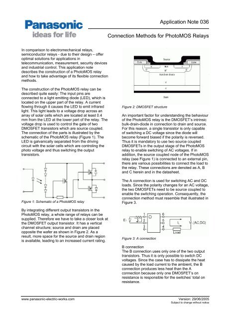
The construction of the <strong>PhotoMOS</strong> relay can be<br />
described quite easily: The input pins are<br />
connected to a light emitting diode (LED), which is<br />
located on the upper part of the relay. A current<br />
flowing through it causes the LED to emit infrared<br />
light. This light leads to a voltage drop across an<br />
array of solar cells which are located at least 0.4<br />
mm from the LED at the lower part of the relay. The<br />
voltage drop is used to control the gate of two<br />
DMOSFET transistors which are source coupled.<br />
The connection of the parts is illustrated by the<br />
schematic of the <strong>PhotoMOS</strong> relay (Figure 1). The<br />
LED is galvanically separated from the driving<br />
circuit with the solar cells which are controling the<br />
photo voltage and thus switching the output<br />
transistors.<br />
Figure 1: Schematic of a <strong>PhotoMOS</strong> relay<br />
By integrating different output transistors in the<br />
<strong>PhotoMOS</strong> relay, a whole range of relays can be<br />
supplied. There<strong>for</strong>e we have to take a closer look at<br />
the DMOSFET output transistor. It has a vertical<br />
channel structure; source and drain are placed<br />
opposite the wafer as shown in Figure 2. As a<br />
result, more space <strong>for</strong> the source and drain region<br />
is available, leading to an increased current rating.<br />
Figure 2: DMOSFET structure<br />
An important factor <strong>for</strong> understanding the behaviour<br />
of the <strong>PhotoMOS</strong> relay is the DMOSFET’s intrinsic<br />
bulk-drain-diode in connection to drain and source.<br />
For this reason, a single transistor is only capable<br />
of switching a DC voltage since the diode will<br />
become <strong>for</strong>ward biased if the polarity is reversed.<br />
Thus it is mandatory to use two source coupled<br />
DMOSFETs in the output stage of the <strong>PhotoMOS</strong><br />
relay to enable switching of AC voltages. If in<br />
addition, the source coupled node of the <strong>PhotoMOS</strong><br />
relay (see Figure 1) is connected to an external pin,<br />
there are various possibilities to connect the load to<br />
the relay. These connections are denoted as A, B<br />
and C herein and in the datasheet.<br />
The A connection is used <strong>for</strong> switching AC and DC<br />
loads. Since the polarity changes <strong>for</strong> an AC voltage,<br />
the two DMOSFETs need to be source coupled to<br />
enable the switching operation. Consequently, the<br />
connection method must resemble that illustrated in<br />
Figure 3.<br />
Figure 3: A connection<br />
B connection<br />
The B connection uses only one of the two output<br />
transistors. Thus it is only possible to switch DC<br />
voltages. Since the case has to dissipate the heat<br />
caused by the load current to the ambient, the B<br />
connection produces less heat than the A<br />
connection because only one DMOSFET’s on<br />
resistance is responsible <strong>for</strong> the switches’ total on<br />
resistance.<br />
www.panasonic-electric-works.com Version: 29/06/2005<br />
Subject to change without notice
Application Note 036<br />
<strong>Connection</strong> <strong>Methods</strong> <strong>for</strong> <strong>PhotoMOS</strong> <strong>Relays</strong><br />
The B connection is shown in Figure 4.<br />
The following table <strong>for</strong> a AQV252G, which is<br />
capable of switching voltages of up to 60 V,<br />
provides a typical overview <strong>for</strong> these kinds of<br />
connections in relationship to on resistance and<br />
load current.<br />
AQV252G<br />
Typical<br />
On resistance<br />
Maximum<br />
Load current<br />
A connection 80 mΩ 2.5 A<br />
B connection 40 mΩ 3 A<br />
Figure 4: B connection<br />
C connection<br />
The C connection uses both output transistors in a<br />
parallel connection (see Figure 5). Consequently,<br />
only DC voltages can be switched (compare also to<br />
B connection). The total on resistance of the relay is<br />
now halved because of the DMOSFET’s parallel<br />
connection when compared to the B connection.<br />
Considering power dissipation again, the current<br />
rating can be further increased because of the<br />
reduced on resistance of the relay.<br />
C connection 20 mΩ 5 A<br />
The above connection methods demonstrate that<br />
<strong>PhotoMOS</strong> relays can be connected to the load in<br />
various ways, offering flexible solutions in regard to<br />
the circuit’s load, the total resistance in the circuit<br />
and the load current. Besides these flexible<br />
connection methods, <strong>PhotoMOS</strong> relays are the<br />
optimal choice when an application requires:<br />
• Low control current<br />
• High switching frequency<br />
• Extremely long lifetime<br />
• Stable on-resistance over lifetime<br />
• High reliability<br />
• Small relay size<br />
• No preferred mounting position<br />
• High vibration and shock resistance<br />
• No switching noise<br />
Figure 5: C connection<br />
The a<strong>for</strong>e mentioned relationships can be<br />
understood quite easily, when one keeps in mind<br />
that maximum power dissipation of the <strong>PhotoMOS</strong><br />
relay, caused by on resistance of the output<br />
transistors and the load current, is limited by the<br />
relay’s case.<br />
www.panasonic-electric-works.com Version: 29/06/2005<br />
Subject to change without notice