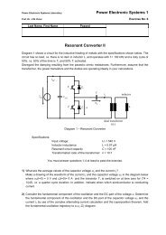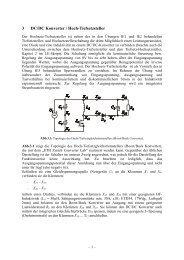
DC/DC Konverter – Grundstrukturen - Power Electronics Systems ...
DC/DC Konverter – Grundstrukturen - Power Electronics Systems ...
DC/DC Konverter – Grundstrukturen - Power Electronics Systems ...

Create successful ePaper yourself
Turn your PDF publications into a flip-book with our unique Google optimized e-Paper software.
<strong>Power</strong> Electronic <strong>Systems</strong> Laboratory <strong>Power</strong> Electronic <strong>Systems</strong> 2<br />
Prof. Dr. J.W. Kolar Solution for Exercise No. 4<br />
Solution <strong>–</strong> Control of a Three-Phase PWM Rectifier System<br />
for the <strong>DC</strong> Link of a Drive System<br />
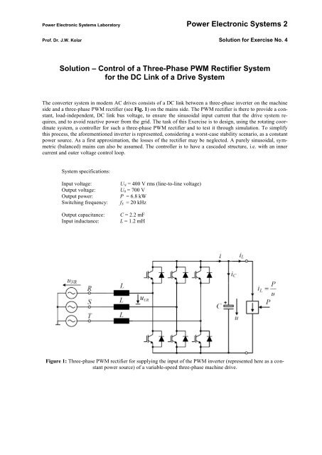
The converter system in modern AC drives consists of a <strong>DC</strong> link between a three-phase inverter on the machine<br />
side and a three-phase PWM rectifier (see Fig. 1) on the mains side. The PWM rectifier is there to provide a constant,<br />
load-independent, <strong>DC</strong> link bus voltage, to ensure the sinusoidal input current that the drive system requires,<br />
and to avoid reactive power from the grid. The task of this Exercise is to design, using the rotating coordinate<br />
system, a controller for such a three-phase PWM rectifier and to test it through simulation. To simplify<br />
this process, the aforementioned inverter is represented, considering a worst-case stability scenario, as a constant<br />
power source. As a first approximation, the losses of the rectifier may be neglected. A purely sinusoidal, symmetric<br />
(balanced) mains can also be assumed. The controller is to have a cascaded structure, i.e. with an inner<br />
current and outer voltage control loop.<br />
System specifications:<br />
Input voltage:<br />
Output voltage:<br />
Output power:<br />
Switching frequency:<br />
Output capacitance:<br />
Input inductance:<br />
U N = 400 V rms (line-to-line voltage)<br />
U 0 = 700 V<br />
P = 6.8 kW<br />
f S = 20 kHz<br />
C = 2.2 mF<br />
L = 1.2 mH<br />
Figure 1: Three-phase PWM rectifier for supplying the input of the PWM inverter (represented here as a constant<br />
power source) of a variable-speed three-phase machine drive.
<strong>Power</strong> Electronic <strong>Systems</strong> Laboratory <strong>Power</strong> Electronic <strong>Systems</strong> 2<br />
Prof. Dr. J.W. Kolar Solution for Exercise No. 4<br />
Part A <strong>–</strong> Calculation & Controller Design<br />
In general, the lengths of the space vectors correspond to the amplitudes of the phase voltages and currents.<br />
1) In order to have the inductor L conduct the required current, the converter must have a certain minimum voltage<br />
vector . This can be determined by looking at the maximum modulation depth at the minimum <strong>DC</strong><br />
link voltage. Consider the steady-state vector diagram:<br />
The voltage across the inductor L is<br />
Figure 2: PWM Rectifier vector diagram<br />
The mains current<br />
power P:<br />
is sinusoidal and in phase with the mains voltage. Knowing this, we can calculate the<br />
| |<br />
⁄ | |<br />
The minimum converter voltage<br />
can be calculated as<br />
| | √| | | |<br />
For the space vector modulation and the fundamental frequency modulation it follows that<br />
| |<br />
√<br />
| |<br />
From this we can calculate the minimum <strong>DC</strong> link voltage:<br />
| | √<br />
| |
<strong>Power</strong> Electronic <strong>Systems</strong> Laboratory <strong>Power</strong> Electronic <strong>Systems</strong> 2<br />
Prof. Dr. J.W. Kolar Solution for Exercise No. 4<br />
2) The block diagram of the controller, including the feed-forward, is given below.<br />
Figure 3: Controller structure including the decoupled current control and feed-forward<br />
3) In dq-coordinates the circuit equations are<br />
If we take into account the cross-coupling and the voltage feed-forward (<br />
controller)<br />
is the control variable of the current<br />
and applying the Laplace transform we obtain the transfer functions:<br />
In addition, there are time delays in the system due to the current measurement and the pulse pattern generation,<br />
as shown in Fig. 4 for the d-component of the mains current ( ).<br />
Figure 4: The d current control loop (i q =0)
Magnitude (dB)<br />
Phase (deg)<br />
<strong>Power</strong> Electronic <strong>Systems</strong> Laboratory <strong>Power</strong> Electronic <strong>Systems</strong> 2<br />
Prof. Dr. J.W. Kolar Solution for Exercise No. 4<br />
These two delay times can be represented as a single additional time constant T 1 =0.1 ms and their combined effect<br />
can be approximated by a 1 st -order low-pass filter (Fig. 5).<br />
The current transfer functions is therefore<br />
Figure 5: Approximation of the total delay time<br />
( )<br />
( )<br />
( )<br />
Since the system has a linear behaviour, linearizing around an operating point can be omitted. The large and<br />
small signal models are identical. If we want to, using a PI Controller, make the crossover frequency 1/20 of the<br />
switching frequency and give the system a phase margin of at least 50°, then<br />
and taking into account the PI controller‟s transfer function,<br />
( )<br />
we get the open-loop transfer function:<br />
( ) ( ) ( )<br />
The desired behaviour of the loop is achieved with the following parameters:<br />
The resulting phase margin is about 55°, which results in stable operation.<br />
100<br />
50<br />
Bode Diagram<br />
G i<br />
G PI<br />
G openl<br />
0<br />
-50<br />
-100<br />
-150<br />
0<br />
-45<br />
-90<br />
-135<br />
-180<br />
10 1 10 2 10 3 10 4 10 5 10 6<br />
Frequency (rad/sec)<br />
Figure 6: Bode plots of the current control system
<strong>Power</strong> Electronic <strong>Systems</strong> Laboratory <strong>Power</strong> Electronic <strong>Systems</strong> 2<br />
Prof. Dr. J.W. Kolar Solution for Exercise No. 4<br />
From the perspective of the significantly slower voltage controller, the closed current control loop can be approximated<br />
as a 1 st -order low-pass filter. The equivalent time constant corresponds to the current control loop‟s<br />
bandwidth:<br />
( )<br />
4) The voltage vectors and the fundamental of the input voltage are shown in Fig. 7 and Fig. 8.<br />
Figure 7: Available space vectors at the converter input<br />
Figure 8: Path of the voltage vector of the fundamental of the input voltage<br />
The maximum converter voltage is limited by the circle inscribed on the hexagon (Fig. 8). Therefore, a limit<br />
should be introduced at the output of the current controller.<br />
| |<br />
√<br />
√
<strong>Power</strong> Electronic <strong>Systems</strong> Laboratory <strong>Power</strong> Electronic <strong>Systems</strong> 2<br />
Prof. Dr. J.W. Kolar Solution for Exercise No. 4<br />
Figure 9: Block diagram of the voltage control loop<br />
5) First, the voltage control transfer function must be determined. Assuming , we can derive the following<br />
circuit equations:<br />
Additionally, the following holds,<br />
( )<br />
and substituting that into the second circuit equation above we get<br />
Now we can perturb and linearize the circuit equations:<br />
̃ ̇<br />
̃<br />
̃<br />
̃<br />
̃ ̇<br />
̃
Phase (deg)<br />
Magnitude (dB)<br />
<strong>Power</strong> Electronic <strong>Systems</strong> Laboratory <strong>Power</strong> Electronic <strong>Systems</strong> 2<br />
Prof. Dr. J.W. Kolar Solution for Exercise No. 4<br />
The perturbation variable ̃<br />
function:<br />
is neglected. Applying the Laplace transform, we arrive at the voltage transfer<br />
( ) ( ) ( )<br />
( )<br />
( )<br />
( )<br />
Adding in the approximation of the control loop (see 3) above), the plant is defined to be<br />
( ) ( ) ( )<br />
( )( )<br />
From the above, the poles and zeros can be clearly seen to be<br />
Since the output starting from a zero in the right half-plane moves first in the „wrong‟ direction, the controller<br />
cannot be too fast <strong>–</strong> otherwise the system becomes unstable. That is, the closer to the origin the right half-plane<br />
zero is, the slower the controller must be. Therefore, the critical operating point is at maximum power, i.e.<br />
P = 6.8 kW. However, in this case, even for that point the zero is at z 1 = 19.6 kHz, which is quite far from the<br />
required crossover frequency of 50 Hz. Therefore the right half-plane zero has practically no influence on the<br />
design of the controller. The PI controller is of the form:<br />
( )<br />
The controller parameters can be derived mathematically (by solving the phase and magnitude equations for k pu<br />
und T nu ) or by using MATLAB:<br />
100<br />
50<br />
Bode Diagram<br />
G str<br />
R<br />
G openl<br />
0<br />
-50<br />
-100<br />
180<br />
90<br />
0<br />
-90<br />
-180<br />
10 0 10 1 10 2 10 3 10 4 10 5<br />
Frequency (rad/sec)<br />
Figure 10: Bode plots of the voltage control system
<strong>Power</strong> Electronic <strong>Systems</strong> Laboratory <strong>Power</strong> Electronic <strong>Systems</strong> 2<br />
Prof. Dr. J.W. Kolar Solution for Exercise No. 4<br />
6) The transfer function of the voltage control loop is, in general, equivalent to the transfer function of a <strong>DC</strong>/<strong>DC</strong><br />
boost converter. To demonstrate this, the boost transfer function is derived below. The circuit equations are<br />
( )( )<br />
( ) ( )( )<br />
Perturbing and linearizing around an operating point we get<br />
̃ ̇<br />
( )<br />
̃<br />
̃ ( ) ̃<br />
( ) ̃ ( ) ̃ ̇<br />
( )<br />
̃<br />
Neglecting the perturbations ̃ and ̃ and simplifying the equations, we get, after a Laplace transform:<br />
( ) ( ) ( )<br />
( ) ( ) ( ) ( )<br />
Finally we get a transfer function that looks the same as that of the voltage loop derived in 5) (see<br />
( ) above):<br />
( )<br />
( )<br />
( )
<strong>Power</strong> Electronic <strong>Systems</strong> Laboratory <strong>Power</strong> Electronic <strong>Systems</strong> 2<br />
Prof. Dr. J.W. Kolar Solution for Exercise No. 4<br />
Part B <strong>–</strong> Simulation<br />
The simulation model of the diode bridge rectifier can be found in the file solution_partB_8.ipes.<br />
7) Phase voltages, phase currents, instantaneous, active, and reactive power, and the compensation currents of<br />
the three-phase system, and the resulting mains currents:
<strong>Power</strong> Electronic <strong>Systems</strong> Laboratory <strong>Power</strong> Electronic <strong>Systems</strong> 2<br />
Prof. Dr. J.W. Kolar Solution for Exercise No. 4<br />
After power factor correction, the resulting active power of the mains phase current is almost unchanged, while<br />
the resulting reactive power is almost all gone. Please note that that for a correct calculation of the reactive power<br />
Q, the circuit must be in steady-state.<br />
The following code is in the JAVA block:<br />
double u_nAlpha = xIN[0];<br />
double u_nBeta = (xIN[1] - xIN[2]) / sqrt(3);<br />
double i_nAlpha = xIN[3];<br />
double i_nBeta = ( xIN[4] - xIN[5] ) / ( sqrt(3) );<br />
// active power:<br />
double P = yOUT[0] = 3.0 / 2.0 * (u_nAlpha * i_nAlpha + u_nBeta * i_nBeta);<br />
// reactive power:<br />
double Q = yOUT[1] = 3.0 / 2.0 * (u_nBeta * i_nAlpha - u_nAlpha * i_nBeta);<br />
// compensating current in alpha-beta-coordinates:<br />
double i_alphaRef = 2.0 / 3.0 * u_nBeta / (u_nAlpha * u_nAlpha + u_nBeta * u_nBeta) * Q;<br />
double i_betaRef = -2.0 / 3.0 * u_nAlpha / (u_nAlpha * u_nAlpha + u_nBeta * u_nBeta) * Q;<br />
// compensating phase currents (r,s,t):<br />
double i_refR = yOUT[2] = i_alphaRef;<br />
double i_refS = yOUT[3] = -0.5 * i_alphaRef + sqrt(3)/2 * i_betaRef;<br />
double i_refT = yOUT[4] = -0.5 * i_alphaRef - sqrt(3)/2 * i_betaRef;<br />
// resulting total phase current:<br />
double i_nAlphaTot = i_nAlpha - i_alphaRef;<br />
double i_nBetaTot = i_nBeta - i_betaRef;<br />
// resulting phase currents (r,s,t):<br />
double i_totR = yOUT[5] = i_nAlphaTot;<br />
double i_totS = yOUT[6] = -0.5 * i_nAlphaTot + sqrt(3)/2 * i_nBetaTot;<br />
double i_totT = yOUT[7] = -0.5 * i_nAlphaTot - sqrt(3)/2 * i_nBetaTot;<br />
// compensated active power:<br />
yOUT[8] = 3.0 / 2.0 * (u_nAlpha * i_nAlphaTot + u_nBeta * i_nBetaTot);<br />
// compensated reactive power:<br />
yOUT[9] = 3.0 / 2.0 * (u_nBeta * i_nAlphaTot - u_nAlpha * i_nBetaTot);
<strong>Power</strong> Electronic <strong>Systems</strong> Laboratory <strong>Power</strong> Electronic <strong>Systems</strong> 2<br />
Prof. Dr. J.W. Kolar Solution for Exercise No. 4<br />
8) a) Plot 1: Input voltage (red), (uncompensated) input current (blue), compensation current (green). Notice here<br />
that the compensation current vector (green) is perpendicular to the voltage space vector lines (red), and is the<br />
vector projection of the current (blue) onto the voltage space vector.<br />
b) Plot 2: die Input voltage (red), compensation current (green), compensated mains current (blue). It can be<br />
seen here that the space vector of the resulting compensated mains current is in phase with the voltage space vector.<br />
9) Transforming the mains voltage and current from coordinates into rotating dq-coordinates:<br />
// Java-Code:<br />
double epsilon = 2*Math.PI * time * 50;<br />
double i_nd = yOUT[12] = sin(epsilon) * i_nBeta + cos(epsilon) * i_nAlpha;<br />
double i_nq = yOUT[13] = cos(epsilon) * i_nBeta - sin(epsilon) * i_nAlpha;<br />
double u_nd = yOUT[14] = u_nAlpha * cos(epsilon) + u_nBeta * sin(epsilon);<br />
double u_nq = yOUT[15] = u_nBeta * cos(epsilon) - u_nAlpha * sin(epsilon);<br />
double Pnd = yOUT[10] = 3.0 / 2.0 * (u_nd * i_nd + u_nq * i_nq);<br />
double Qnd = yOUT[11] = 3.0 / 2.0 * (u_nq * i_nd - u_nd * i_nq);
<strong>Power</strong> Electronic <strong>Systems</strong> Laboratory <strong>Power</strong> Electronic <strong>Systems</strong> 2<br />
Prof. Dr. J.W. Kolar Solution for Exercise No. 4<br />
10) GeckoCIRCUITS model of the three-phase PWM rectifier:<br />
11) The GeckoCIRCUITS implementation of the current controller, with the output capacitor replaced by a constant<br />
voltage source, can be found in the model file solution_partB_11.ipes.<br />
12) The GeckoCIRCUITS implementation of the voltage controller is given in the model file solution_partB_12-<br />
14.ipes:
<strong>Power</strong> Electronic <strong>Systems</strong> Laboratory <strong>Power</strong> Electronic <strong>Systems</strong> 2<br />
Prof. Dr. J.W. Kolar Solution for Exercise No. 4<br />
Space vector diagrams: Left: Transient, the current in the inductor starts at zero. Right: Steady-state.<br />
Blue: mains voltage; red: converter input voltage; green: input voltage averaged over a switching period.
<strong>Power</strong> Electronic <strong>Systems</strong> Laboratory <strong>Power</strong> Electronic <strong>Systems</strong> 2<br />
Prof. Dr. J.W. Kolar Solution for Exercise No. 4<br />
13) If the initial voltage of the output capacitor is too small, e.g. 450 V, the controller cannot stabilize the system<br />
(see simulation results below). This happens because the output voltage is too low for the inductor to conduct the<br />
required current (see the solution for 1) and the calculated there).<br />
This problem can be solved by defining a “start-up” procedure for the system, which would make sure that the<br />
output is pre-charged to the minimum required voltage, and only then allowing the voltage and current controllers<br />
to operate.<br />
14) Java code for discrete sampling:<br />
// ------------ Exercise 13 - discrete output ----------------<br />
if(xIN[6] < 1) { // calculate discrete, sampled output:<br />
return yOUT;<br />
}<br />
double i_ndTrig = yOUT[12] = i_nd;<br />
double i_nqTrig = yOUT[13] = i_nq;<br />
double u_ndTrig = yOUT[14] = u_nd;<br />
double u_nqTrig = yOUT[15] = u_nq;<br />
return yOUT;<br />
xIN[6] above is the “trigger” input, and if it is low (i.e. off), the JAVA block function returns immediately, returning<br />
the old, previously stored value of the output. The current and voltage values sent to the output of the<br />
JAVA block are therefore only updated when the trigger signal is high (i.e. on <strong>–</strong> greater than or equal to 1). In<br />
the following simulation results you can see the difference between the continuous (left) and the discrete (sampled)<br />
signal (right):
<strong>Power</strong> Electronic <strong>Systems</strong> Laboratory <strong>Power</strong> Electronic <strong>Systems</strong> 2<br />
Prof. Dr. J.W. Kolar Solution for Exercise No. 4<br />
The advantage of discrete sampling is that the switching ripple is completely filtered out, since the sampling rate<br />
is equal to the switching frequency. The controller therefore receives a much more stable signal.<br />
The disadvantage is that the discrete sampling introduces a delay of T S / 2.<br />
With each increase in delay, there is more instability in the current waveforms. The instability is a result of the<br />
increased phase-shift introduced into the system by the increased delay. A delay longer than approximately<br />
125 sec (+ 50 sec sampling delay) causes the voltage controller to become completely unstable, and the converter<br />
no longer operates properly (see simulation results below).<br />
Delay: 110 sec
<strong>Power</strong> Electronic <strong>Systems</strong> Laboratory <strong>Power</strong> Electronic <strong>Systems</strong> 2<br />
Prof. Dr. J.W. Kolar Solution for Exercise No. 4<br />
Delay: 125 sec