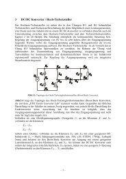
Bi-Directional Isolated DC-DC Converter for Next-Generation Power ...
Bi-Directional Isolated DC-DC Converter for Next-Generation Power ...
Bi-Directional Isolated DC-DC Converter for Next-Generation Power ...

You also want an ePaper? Increase the reach of your titles
YUMPU automatically turns print PDFs into web optimized ePapers that Google loves.
until the <strong>DC</strong>-link voltage is blocked.<br />
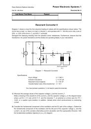
IV. DESIGN OF <strong>DC</strong>-<strong>DC</strong> CONVERTER<br />
In the following the design of the SiC <strong>DC</strong>-<strong>DC</strong> converter<br />
<strong>for</strong> an output power of 20kW is presented. For calculating<br />
the switching and conduction losses measurement results <strong>for</strong><br />
the SiC JFET are presented. Moreover, the design of the high<br />
voltage trans<strong>for</strong>mer will be discussed in detail and a 3D model<br />
of the converter is presented.<br />
A. Experimental Results<br />
For an application in the distribution system with the<br />
specifications given in table I the HV switch consists of two<br />
modules B and one module A, resulting in a total blocking<br />
voltage of 9kV. There, a safety voltage margin is included <strong>for</strong><br />
dynamic voltage balancing. In the following these three series<br />
connected modules are denoted as one HV switch.<br />
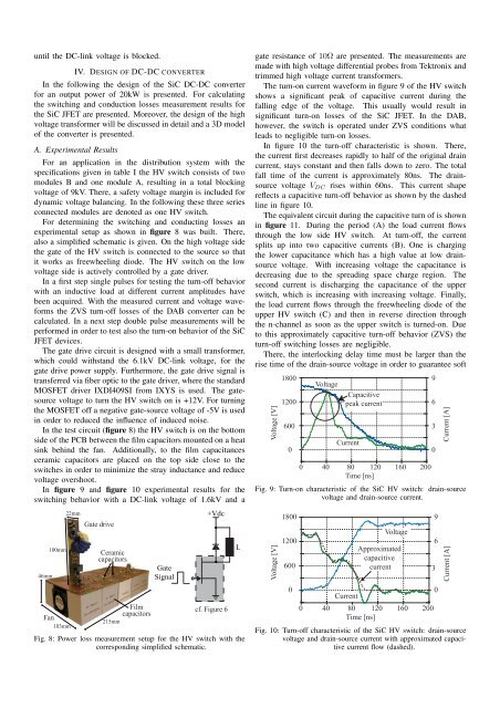
For determining the switching and conducting losses an<br />
experimental setup as shown in figure 8 was built. There,<br />
also a simplified schematic is given. On the high voltage side<br />
the gate of the HV switch is connected to the source so that<br />
it works as freewheeling diode. The HV switch on the low<br />
voltage side is actively controlled by a gate driver.<br />
In a first step single pulses <strong>for</strong> testing the turn-off behavior<br />
with an inductive load at different current amplitudes have<br />
been acquired. With the measured current and voltage wave<strong>for</strong>ms<br />
the ZVS turn-off losses of the DAB converter can be<br />
calculated. In a next step double pulse measurements will be<br />
per<strong>for</strong>med in order to test also the turn-on behavior of the SiC<br />
JFET devices.<br />
The gate drive circuit is designed with a small trans<strong>for</strong>mer,<br />
which could withstand the 6.1kV <strong>DC</strong>-link voltage, <strong>for</strong> the<br />
gate drive power supply. Furthermore, the gate drive signal is<br />
transferred via fiber optic to the gate driver, where the standard<br />
MOSFET driver IXDI409SI from IXYS is used. The gatesource<br />
voltage to turn the HV switch on is +12V. For turning<br />
the MOSFET off a negative gate-source voltage of -5V is used<br />
in order to reduced the influence of induced noise.<br />
In the test circuit (figure 8) the HV switch is on the bottom<br />
side of the PCB between the film capacitors mounted on a heat<br />
sink behind the fan. Additionally, to the film capacitances<br />
ceramic capacitors are placed on the top side close to the<br />
switches in order to minimize the stray inductance and reduce<br />
voltage overshoot.<br />
In figure 9 and figure 10 experimental results <strong>for</strong> the<br />
switching behavior with a <strong>DC</strong>-link voltage of 1.6kV and a<br />
46mm<br />
100mm<br />
Fan<br />
103mm<br />
22mm<br />
Gate drive<br />
Ceramic<br />
capacitors<br />
215mm<br />
Film<br />
capacitors<br />
Gate<br />
Signal<br />
+Vdc<br />
cf. Figure 6<br />
Fig. 8: <strong>Power</strong> loss measurement setup <strong>for</strong> the HV switch with the<br />
corresponding simplified schematic.<br />
L<br />
gate resistance of 10Ω are presented. The measurements are<br />
made with high voltage differential probes from Tektronix and<br />
trimmed high voltage current trans<strong>for</strong>mers.<br />
The turn-on current wave<strong>for</strong>m in figure 9 of the HV switch<br />
shows a significant peak of capacitive current during the<br />
falling edge of the voltage. This usually would result in<br />
significant turn-on losses of the SiC JFET. In the DAB,<br />
however, the switch is operated under ZVS conditions what<br />
leads to negligible turn-on losses.<br />
In figure 10 the turn-off characteristic is shown. There,<br />
the current first decreases rapidly to half of the original drain<br />
current, stays constant and then falls down to zero. The total<br />
fall time of the current is approximately 80ns. The drainsource<br />
voltage V <strong>DC</strong> rises within 60ns. This current shape<br />
reflects a capacitive turn-off behavior as shown by the dashed<br />
line in figure 10.<br />
The equivalent circuit during the capacitive turn of is shown<br />
in figure 11. During the period (A) the load current flows<br />
through the low side HV switch. At turn-off, the current<br />
splits up into two capacitive currents (B). One is charging<br />
the lower capacitance which has a high value at low drainsource<br />
voltage. With increasing voltage the capacitance is<br />
decreasing due to the spreading space charge region. The<br />
second current is discharging the capacitance of the upper<br />
switch, which is increasing with increasing voltage. Finally,<br />
the load current flows through the freewheeling diode of the<br />
upper HV switch (C) and then in reverse direction through<br />
the n-channel as soon as the upper switch is turned-on. Due<br />
to this approximately capacitive turn-off behavior (ZVS) the<br />
turn-off switching losses are negligible.<br />
There, the interlocking delay time must be larger than the<br />
rise time of the drain-source voltage in order to guarantee soft<br />
Voltage [V]<br />
1800<br />
1200<br />
600<br />
0<br />
Voltage<br />
Capacitive<br />
peak current<br />
Current<br />
0 40 80 120 160 200<br />
Time [ns]<br />
Fig. 9: Turn-on characteristic of the SiC HV switch: drain-source<br />
voltage and drain-source current.<br />
Voltage [V]<br />
1800<br />
1200<br />
600<br />
0<br />
Current<br />
Voltage<br />
Approximated<br />
capacitive<br />
current<br />
0 40 80 120 160 200<br />
Time [ns]<br />
Fig. 10: Turn-off characteristic of the SiC HV switch: drain-source<br />
voltage and drain-source current with approximated capacitive<br />
current flow (dashed).<br />
9<br />
6<br />
3<br />
0<br />
3<br />
9<br />
6<br />
0<br />
Current [A]<br />
Current [A]