Experiment 4 Advanced op-amp designs
Experiment 4 Advanced op-amp designs
Experiment 4 Advanced op-amp designs

You also want an ePaper? Increase the reach of your titles
YUMPU automatically turns print PDFs into web optimized ePapers that Google loves.
<strong>Experiment</strong> 4<br />
<strong>Advanced</strong> <strong>op</strong>-<strong>amp</strong> <strong>designs</strong><br />
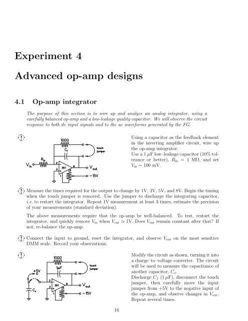
4.1 Op-<strong>amp</strong> integrator<br />
The purpose of this section is to wire up and analyze an analog integrator, using a<br />
carefully balanced<strong>op</strong>-<strong>amp</strong>and a low-leakagequality capacitor. We will observe the circuit<br />
response to both dc input signals and to the ac waveforms generated by the FG.<br />
☛✟<br />
✡! ✠<br />
Using a capacitor as the feedback element<br />
in the inverting <strong>amp</strong>lifier circuit, wire up<br />
the <strong>op</strong>-<strong>amp</strong> integrator.<br />
Use a1µFlow–leakagecapacitor (10%tolerance<br />
or better), R in = 1 MΩ, and set<br />
V in = 100 mV.<br />
☛✟<br />
✡! ✠Measure the times required for the output to change by 1V, 3V, 5V, and 8V. Begin the timing<br />
when the touch jumper is removed. Use the jumper to discharge the integrating capacitor,<br />
i.e. to restart the integrator. Repeat 1V measurement at least 3 times, estimate the precision<br />
of your measurements (standard deviation).<br />
The above measurements require that the <strong>op</strong>-<strong>amp</strong> be well-balanced. To test, restart the<br />
integrator, and quickly remove V in when V out ≃ 1V. Does V out remain constant after that? If<br />
not, re-balance the <strong>op</strong>-<strong>amp</strong>.<br />
☛✟<br />
✡! ✠Connect the input to ground, reset the integrator, and observe V out on the most sensitive<br />
DMM scale. Record your observations.<br />
☛✟<br />
✡! ✠<br />
Modifythecircuit asshown, turningitinto<br />
a charge–to–voltage converter. The circuit<br />
will be used to measure the capacitance of<br />
another capacitor, C x .<br />
Discharge C f (1µF), disconnect the touch<br />
jumper, then carefully move the input<br />
jumper from +5V to the negative input of<br />
the <strong>op</strong>-<strong>amp</strong>, and observe changes in V out .<br />
Repeat several times.<br />
16
4.2. OP-AMP DIFFERENTIATOR 17<br />
? Compare the measured value of the ratio C f /C x with that obtained by a direct reading of the<br />
capacitance meter.<br />
☛✟<br />
✡! ✠<br />
Use FG to provide a square–wave input to<br />
theintegrator. UseR in = 1MΩandsetthe<br />
frequency to about 1 kHz. Choose the C f<br />
valueappr<strong>op</strong>riateforthisfrequency. Monitor<br />
both the input and the output with the<br />
sc<strong>op</strong>e. Make sure you adjust FG to have<br />
a zero DC offset. Alternatively, you may<br />
want to use a small capacitor (≃ 1µF) in<br />
series with FG, to remove the dc component<br />
from the input.<br />
☛✟<br />
✡! ✠Sketch and explain the observed waveforms.<br />
4.2 Op-<strong>amp</strong> differentiator<br />
By interchanging the resistor and capacitor of the <strong>op</strong>-<strong>amp</strong> integrator, we obtain an <strong>op</strong><strong>amp</strong><br />
differentiator. We will analyze its response to various waveforms of the FG.<br />
Do not remove the circuit of the previous section; you may want to re-use it in Section<br />
4.3.<br />
☛✟<br />
✡! ✠<br />
Wire up an <strong>op</strong>-<strong>amp</strong> differentiator as<br />
shown. In a dual-353 package you may<br />
choose either of the two <strong>op</strong>-<strong>amp</strong>s (pins<br />
2,3,1 or 6,5,7). The 100 pF capacitor is included<br />
to provide noise stability. For this<br />
circuit,<br />
V out = −RC dV in<br />
dt<br />
Set the FG to 5V peak–to–peak 1 kHz triangular<br />
wave and connect it as V in .<br />
☛✟<br />
✡! ✠Sketch the input and output waveforms, including the pr<strong>op</strong>er scales. Make sure your sc<strong>op</strong>e is<br />
on a calibrated setting.<br />
Calculate and record the sl<strong>op</strong>e of the input triangular wave. Also, record the <strong>amp</strong>litude of<br />
the square wave at the output.<br />
? Calculate the expected theoretical value for the differentiator output and compare it to the<br />
experimental value.<br />
☛✟<br />
✡! ✠Change the FG to square wave setting. Sketch the observed waveforms.<br />
4.3 Difference <strong>amp</strong>lifier<br />
The purpose of this section is to introduce precision <strong>amp</strong>lifiers and to learn to distinguish<br />
differential and common mode signals.<br />
Ref: Simpson, Ch. 9–10, esp. Sec. 9.8.7, 10.4; Faissler, Ch. 31 (review); Malmstadt et<br />
al., Ch. 8.1.
18 EXPERIMENT 4. ADVANCED OP-AMP DESIGNS<br />
☛✟<br />
✡! ✠<br />
Wire up the difference <strong>amp</strong>lifier as shown:<br />
Balance the <strong>op</strong>-<strong>amp</strong> by connecting both V 1<br />
and V 2 to ground and adjusting the offset<br />
potentiometer until V out = 0.<br />
Leaving V 2 grounded, vary V 1 (several values<br />
between +1V and −1V) and measure<br />
V out .<br />
? Calculatetheaveragegainofthe<strong>amp</strong>lifier. Inthismeasurement, whichcomponentsdetermine<br />
the gain of the <strong>amp</strong>lifier? How does the measured value compare with the theoretical one?<br />
☛✟<br />
✡! ✠Connect V 2 to a constant +1V source and repeat the above two steps.<br />
☛✟<br />
✡! ✠Connect both V 1 and V 2 to the same variable voltage source; measure V out for several values<br />
of V 1 = V 2 between +1V and −1V.<br />
? Plot V out vs. V 1 and determine the value of the common mode gain from the plot.<br />
? Interpret your data in terms of the imbalance of the resistance ratios of the two pairs of<br />
resistors determining the gain, for the inverting and for the non-inverting input. Which pair<br />
has the higher gain and by how much? How could this common mode gain be reduced?<br />
? Calculate the common-mode rejection ratio (CMRR) for your difference <strong>amp</strong>lifier. Calculate<br />
the maximum common-mode signal the <strong>amp</strong>lifier can accept if a 100 mV signal is to<br />
be <strong>amp</strong>lified with an error of less than 0.1%.
4.4. INSTRUMENTATION AMPLIFIER 19<br />
4.4 Instrumentation <strong>amp</strong>lifier<br />
The purpose of this section is to combine the advantages of a difference input with the<br />
high input resistance of the voltage follower in a complete instrumentation <strong>amp</strong>lifier.<br />
☛✟<br />
✡! ✠Wireuptheinstrumentation<strong>amp</strong>lifierasshown(addtheinputvoltagefollowerstotheexisting<br />
circuit).<br />
Check the offset of the instrumentation <strong>amp</strong>lifier and adjust the difference <strong>amp</strong>lifier offset<br />
potentiometer if needed. Measure V out for various values of V 1 and V 2 so that you will be able<br />
to determine the difference gain and the common mode rejection ratio of the instrumentation<br />
<strong>amp</strong>lifier. Be sure you have taken sufficient data to perform your calculations.<br />
? Describe the reasoning you used in selecting the values for V 1 and V 2 . From these data,<br />
determine the gain and the CMRR. Explain your interpretation of the data. Compare your<br />
results with the expected values.<br />
4.5 Logarithmic <strong>amp</strong>lifier<br />
Using a non-linear feedback element with an <strong>op</strong>-<strong>amp</strong> (e.g. a pn–junction diode) produces<br />
startlingly different transfer functions. Logarithmic <strong>amp</strong>lifiers serve as the basis for<br />
circuits such as analog multipliers studied in Section 4.6.<br />
☛✟<br />
✡! ✠<br />
Carefully balance a 351 <strong>op</strong>-<strong>amp</strong>. Then<br />
wire the logarithmic <strong>amp</strong>lifier (log <strong>amp</strong>),<br />
using a signal diode as the feedback element.<br />
☛✟<br />
✡! ✠Measure V out as a function of V in and R in :
20 EXPERIMENT 4. ADVANCED OP-AMP DESIGNS<br />
? Plot logI in vs. V out .<br />
V in R in I in V out<br />
10.0mV 1MΩ<br />
10.0mV 100kΩ<br />
100.0mV 100kΩ<br />
1.0V 100kΩ<br />
10.0V 100kΩ<br />
10.0V 10kΩ<br />
For all but very small forward bias voltages, the current through a diode varies exponentially<br />
with the applied voltage:<br />
I ≃ I i e eV/ηkT<br />
where η is an empirical parameter (∼ 2 for Si, 1 for Ge diodes), and I i is the intrinsic current<br />
at zero bias.<br />
Apply circuit analysis (Simpson, Sec. 9.7) to your logarithmic <strong>amp</strong>lifier and verify that the<br />
same relationship holds for the measured I in and V out .<br />
Fit your data to the above equation and determine the parameters η and I i for your diode.<br />
Can you tell if this is a Si or a Ge diode?<br />
4.6 Analog multiplier<br />
Combining log <strong>amp</strong>s with adding <strong>amp</strong>s allows one to build analog multipliers and other<br />
components of analog computers (for a review, see Faissler, Ch. 30). Here we examine<br />
the transfer functions of one such commercial device, AD534.<br />
AD534 is internally trimmed and does not<br />
require external trimmer potentiometers.<br />
Its pinout is shown on the left.<br />
☛✟<br />
✡! ✠For multiplication, use the fixed +10V supply from the job board as the X 1 input and use<br />
several fixed voltages from the reference job board as the Y 1 input (+10V, −10V, −1V, +1V).<br />
Connect the Z 1 input to the output. Connect the X 2 , Y 2 , and Z 2 inputs to common. Test<br />
the multiplier in all four quadrants by applying voltages of both polarities in the range of<br />
±10V. The multiplier transfer function should be V out = (V x ×V y )/10. Include in your data<br />
set (X 1 ,Y 1 ) values of (+10,0), (0,0), and (0,+10).<br />
? Offsets modify the multiplier equation:<br />
V out = V out (0) +0.1× [ V x −V (0)<br />
x<br />
] [ ]<br />
× Vy −V y<br />
(0)<br />
where V (0)<br />
x , V (0)<br />
y , and V out (0) are the X, Y, and output offsets, respectively. Use your data to<br />
evaluate each of the offsets. Explain how magnitude of offset–induced errors changes with X<br />
and Y input levels.
4.6. ANALOG MULTIPLIER 21<br />
☛✟<br />
✡! ✠To obtain an output voltage pr<strong>op</strong>ortional to the square of an input voltage, connect both X 1<br />
and Y 1 inputs to the same voltage source and the X 2 and Y 2 inputs to common. The Z 1 input<br />
remains connected to the output. Test the circuit over a ±10V range of voltages and compare<br />
to the expected V out = 0.1×V 2 in .<br />
☛✟<br />
✡! ✠The “squared voltage”output can be plotted against the input with the xy–mode of the<br />
oscillosc<strong>op</strong>e. Substitute the output of the FG set in the sine wave mode as the source in the<br />
squaring circuit wired above. Connect the multiplier output to the vertical sc<strong>op</strong>e input and<br />
the FG output to the horizontal. Use a 10Hz sine wave signal. Sketch the resulting display.<br />
☛✟<br />
✡! ✠Nowusethedual-tracemodeto observe thewaveforms oftheinput andoutputsignals. Sketch<br />
a representative display and indicate the position of OV for each waveform.<br />
? Explain the relationship of the frequencies and the DC components of the input and output<br />
waveforms.<br />
Optional: analog division<br />
☛✟<br />
✡! ✠To obtain division, connect the multiplier output to the Y 2 input. Now Z 1 is no longer<br />
connected to the output, and Z 2 is no longer grounded. In this configuration:<br />
V out = 10× V(Z 2)−V(Z 1 )<br />
V(X 1 )−V(X 2 ) +V(Y 1)<br />
Measure V out for several values of V(Z 2 ) − V(Z 1 ) and V(X 1 ) − V(X 2 ). For simplicity, you<br />
may want to ground Z 1 , X 2 , and Y 1 . Make sure you keep V(X 1 ) −V(X 2 ) positive (see the<br />
spec sheets of AD534).<br />
? The output limits of AD534 are ±11V. Calculate and plot the minimum value for V(X 1 )−<br />
V(X 2 ) as a function of V(Z 2 )−V(Z 1 ) over the V(Z) range of ±10V.