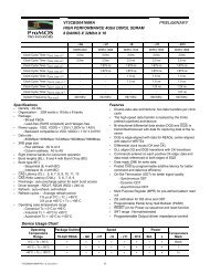
V54C3128(16/80/40)4VC 128Mbit SDRAM 3.3 VOLT, TSOP II / BGA ...
V54C3128(16/80/40)4VC 128Mbit SDRAM 3.3 VOLT, TSOP II / BGA ...
V54C3128(16/80/40)4VC 128Mbit SDRAM 3.3 VOLT, TSOP II / BGA ...

You also want an ePaper? Increase the reach of your titles
YUMPU automatically turns print PDFs into web optimized ePapers that Google loves.
ProMOS TECHNOLOGIES<br />
<strong>V54C3128</strong>(<strong>16</strong>/<strong>80</strong>/<strong>40</strong>)<strong>4VC</strong><br />
Timing Diagrams (Cont’d)<br />
15. Random Column Read ( Page within same Bank)<br />
15.1 CAS Latency = 2<br />
15.2 CAS Latency = 3<br />
<strong>16</strong>. Random Column Write ( Page within same Bank)<br />
<strong>16</strong>.1 CAS Latency = 2<br />
<strong>16</strong>.2 CAS Latency = 3<br />
17. Random Row Read ( Interleaving Banks) with Precharge<br />
17.1 CAS Latency = 2<br />
17.2 CAS Latency = 3<br />
18. Random Row Write ( Interleaving Banks) with Precharge<br />
18.1 CAS Latency = 2<br />
18.2 CAS Latency = 3<br />
19. Precharge Termination of a Burst<br />
19.1 CAS Latency = 2<br />
19.2 CAS Latency = 3<br />
20. Full Page Burst Operation<br />
20.1 Full Page Burst Read, CAS Latency = 2<br />
20.2 Full Page Burst Read, CAS Latency = 3<br />
21. Full Page Burst Operation<br />
21.1 Full Page Burst Write, CAS Latency = 2<br />
21.2 Full Page Burst Write, CAS Latency = 3<br />
<strong>V54C3128</strong>(<strong>16</strong>/<strong>80</strong>/<strong>40</strong>)<strong>4VC</strong> Rev. 1.3 November 2008<br />
21