V54C3128(16/80/40)4VC 128Mbit SDRAM 3.3 VOLT, TSOP II / BGA ...
V54C3128(16/80/40)4VC 128Mbit SDRAM 3.3 VOLT, TSOP II / BGA ...
V54C3128(16/80/40)4VC 128Mbit SDRAM 3.3 VOLT, TSOP II / BGA ...

You also want an ePaper? Increase the reach of your titles
YUMPU automatically turns print PDFs into web optimized ePapers that Google loves.
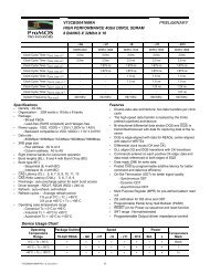
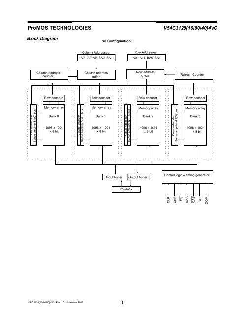
ProMOS TECHNOLOGIES<br />
<strong>V54C3128</strong>(<strong>16</strong>/<strong>80</strong>/<strong>40</strong>)<strong>4VC</strong><br />
Block Diagram<br />
x8 Configuration<br />
Column Addresses<br />
Row Addresses<br />
A0 - A9, AP, BA0, BA1<br />
A0 - A11, BA0, BA1<br />
Column address<br />
counter<br />
Column address<br />
buffer<br />
Row address<br />
buffer<br />
Refresh Counter<br />
Row decoder<br />
Row decoder<br />
Row decoder<br />
Row decoder<br />
Column decoder<br />
Sense amplifier & I(O) bus<br />
Memory array<br />
Bank 0<br />
<strong>40</strong>96 x 1024<br />
x 8 bit<br />
Column decoder<br />
Sense amplifier & I(O) bus<br />
Memory array<br />
Bank 1<br />
<strong>40</strong>96 x 1024<br />
x 8 bit<br />
Column decoder<br />
Sense amplifier & I(O) bus<br />
Memory array<br />
Bank 2<br />
<strong>40</strong>96 x 1024<br />
x 8 bit<br />
Column decoder<br />
Sense amplifier & I(O) bus<br />
Memory array<br />
Bank 3<br />
<strong>40</strong>96 x 1024<br />
x 8 bit<br />
Input buffer<br />
Output buffer<br />
Control logic & timing generator<br />
I/O 0 -I/O 7<br />
CLK<br />
CKE<br />
CS<br />
RAS<br />
CAS<br />
WE<br />
DQM<br />
<strong>V54C3128</strong>(<strong>16</strong>/<strong>80</strong>/<strong>40</strong>)<strong>4VC</strong> Rev. 1.3 November 2008<br />
9