wlcsp-11-p2 - Ricoh
wlcsp-11-p2 - Ricoh
wlcsp-11-p2 - Ricoh

Create successful ePaper yourself
Turn your PDF publications into a flip-book with our unique Google optimized e-Paper software.
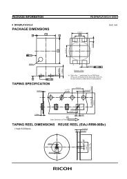
PACKAGE INFORMATION<br />
PE-WLCSP-<strong>11</strong>-P2-07<strong>11</strong>06<br />
• WLCSP-<strong>11</strong>-P2<br />
PACKAGE DIMENSIONS<br />
Unit: mm<br />
A<br />
2.37<br />
B<br />
φ0.16±0.03<br />
φ0.05 M S AB<br />
3<br />
× 4<br />
0.05<br />
1.47<br />
2<br />
0.5<br />
1<br />
INDEX<br />
0.10 S<br />
D C B A<br />
0.5<br />
0.70±0.02<br />
Bottom View<br />
S<br />
0.06 S<br />
TAPING SPECIFICATION<br />
0.08±0.03<br />
0.18±0.1<br />
1.5 +0.1<br />
0<br />
4.0±0.1<br />
2.0±0.05<br />
1.75±0.1<br />
1.57<br />
2.47<br />
3.5±0.05<br />
8.0±0.3<br />
1.5Max.<br />
Dummy Pocket<br />
0.5±0.1<br />
4.0±0.1<br />
E2<br />
User Direction of Feed<br />
TAPING REEL DIMENSIONS REUSE REEL (EIAJ-RRM-08Bc)<br />
(1reel=4000pcs)<br />
<strong>11</strong>.4±1.0<br />
9.0±0.3<br />
∅13±0.2<br />
2±0.5<br />
21±0.8<br />
∅ 60 +1 0<br />
0<br />
−1.5<br />
∅180
PACKAGE INFORMATION<br />
PE-WLCSP-<strong>11</strong>-P2-07<strong>11</strong>06<br />
POWER DISSIPATION (WLCSP-<strong>11</strong>-P2)<br />
This specification is at mounted on board. Power Dissipation (PD) depends on conditions of mounting on board.<br />
This specification is based on the measurement at the condition below:<br />
Measurement Conditions<br />
Standard Land Pattern<br />
Environment<br />
Mounting on Board (Wind velocity=0m/s)<br />
Board Material<br />
Glass cloth epoxy plastic (Double sided)<br />
Board Dimensions<br />
40mm × 40mm × 1.6mm<br />
Copper Ratio Top side : Approx. 80%, Back side : Approx. 90%<br />
Through-hole<br />
φ0.6mm × 31pcs<br />
Measurement Result<br />
Power Dissipation<br />
Thermal Resistance<br />
Thermal Resistance<br />
(Topt=25°C, Tjmax=125°C)<br />
Standard Land Pattern<br />
1000mW<br />
θja=(125−25°C)/1W=100°C/W<br />
θjc=7°C/W<br />
1200<br />
40<br />
Power Dissipation PD(mW)<br />
1000<br />
800<br />
600<br />
400<br />
200<br />
1000<br />
On Board<br />
40<br />
0<br />
0 25 50 75 85 100 125 150<br />
Ambient Temperature (°C)<br />
Power Dissipation<br />
Measurement Board Pattern<br />
IC Mount Area Unit : mm
PACKAGE INFORMATION<br />
PE-WLCSP-<strong>11</strong>-P2-07<strong>11</strong>06<br />
RECOMMENDED LAND PATTERN<br />
Solder Mask<br />
(resist)<br />
Copper Pad<br />
Substrate<br />
NSMD<br />
SMD<br />
(Unit : mm)<br />
NSMD and SMD Pad Definition<br />
Pad definition Copper Pad Solder Mask Opening<br />
NSMD (Non-Solder Mask defined) 0.20mm Min. 0.30mm<br />
SMD (Solder Mask defined) Min. 0.30mm 0.20mm<br />
* Pad layout and size can be modified by customers material, equipment, method.<br />
* Please adjust pad layout according to your conditions.<br />
* Recommended Stencil Aperture Size....ø0.3mm<br />
* Since lead free WL-CSP components are not compatible with the tin/lead solder process, you shall not mount lead free WL-CSP<br />
components using the tin/lead solder paste.