CD3 User Guide - EKF
CD3 User Guide - EKF
CD3 User Guide - EKF

Create successful ePaper yourself
Turn your PDF publications into a flip-book with our unique Google optimized e-Paper software.
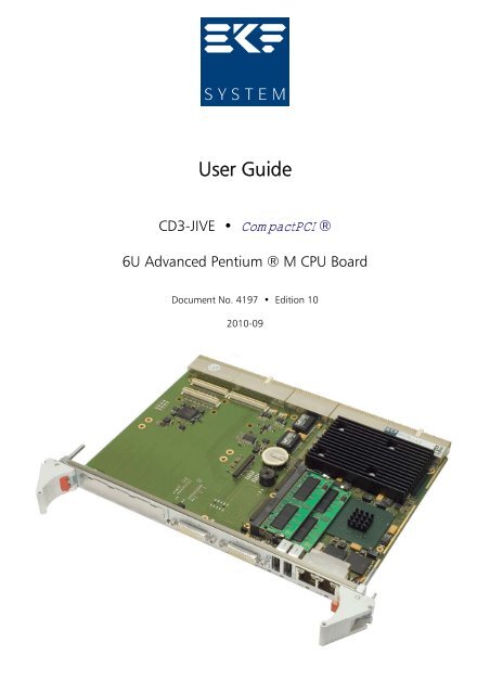
<strong>User</strong> <strong>Guide</strong><br />
<strong>CD3</strong>-JIVE • CompactPCI ®<br />
6U Advanced Pentium ® M CPU Board<br />
Document No. 4197 • Edition 10<br />
2010-09
<strong>User</strong> <strong>Guide</strong> <strong>CD3</strong>-JIVE • Advanced CompactPCI 6U Pentium® M CPU Board<br />
Contents<br />
About this Manual ........................................................... 4<br />
Edition History......................................................... 4<br />
Related Documents ..................................................... 5<br />
Nomenclature ......................................................... 5<br />
Trade Marks .......................................................... 5<br />
Legal Disclaimer - Liability Exclusion ......................................... 5<br />
<strong>CD3</strong>-JIVE Features ........................................................... 6<br />
Feature Summary ...................................................... 6<br />
Short Description <strong>CD3</strong>-JIVE ............................................... 9<br />
Block Diagram <strong>CD3</strong>-JIVE ................................................ 16<br />
Top View Component Assembly <strong>CD3</strong>-JIVE ................................... 18<br />
CDT-RIO Rear I/O Transition Module ....................................... 19<br />
Short Description ................................................ 19<br />
Block Diagram CDT-RIO ........................................... 21<br />
Assembly Drawing CDT-RIO ................................... 21<br />
<strong>CD3</strong>-JIVE On-Board Elements............................................. 23<br />
Strapping Headers ............................................... 23<br />
Connectors & Sockets ............................................. 23<br />
LED Indicators................................................... 23<br />
<strong>CD3</strong>-JIVE Front Panel Elements ........................................... 24<br />
Microprocessor ....................................................... 25<br />
Thermal Considerations ................................................. 26<br />
Main Memory ........................................................ 26<br />
LAN Subsystem ....................................................... 27<br />
Serial ATA Interface (SATA) .............................................. 28<br />
Enhanced IDE Interface ................................................. 28<br />
Graphics Subsystem ................................................... 29<br />
Real-Time Clock....................................................... 30<br />
Universal Serial Bus (USB) ............................................... 30<br />
LPC Super-I/O Interface ................................................. 30<br />
Reset/Watchdog ...................................................... 31<br />
Firmware Hub (Flash BIOS) .............................................. 31<br />
Mezzanine Interfaces................................................... 32<br />
PG (Power Good) LED .................................................. 32<br />
HD (Hard Disk Activity) LED .............................................. 32<br />
GP (General Purpose) LED ............................................... 32<br />
Hot Swap Detection ................................................... 32<br />
Power Supply Status (DEG#, FAL#) ........................................ 33<br />
PXI Trigger Signals..................................................... 33<br />
GPIO Signals ......................................................... 33<br />
Rear I/O Options ...................................................... 34<br />
Installing and Replacing Components............................................ 35<br />
Before You Begin...................................................... 35<br />
Installing the Board .................................................... 36<br />
Removing the Board ................................................... 37<br />
EMC Recommendations................................................. 38<br />
© <strong>EKF</strong> -2- ekf.com
<strong>User</strong> <strong>Guide</strong> <strong>CD3</strong>-JIVE • Advanced CompactPCI 6U Pentium® M CPU Board<br />
Installing or Replacing the Memory Modules ................................. 39<br />
Replacement of the Battery .............................................. 39<br />
Technical Reference ......................................................... 40<br />
Local PCI Devices ...................................................... 40<br />
Local SMB Devices ..................................................... 41<br />
Hardware Monitor LM87 ................................................ 41<br />
GPIO Usage.......................................................... 42<br />
GPIO Usage ICH6 ................................................ 42<br />
GPIO Usage FWH ................................................ 43<br />
GPIO Usage SIO ................................................. 44<br />
Configuration Jumpers ................................................. 45<br />
Reset Jumper BIOS CMOS RAM Values (J-GP) ........................... 45<br />
Reset Jumper ICH6 RTC Core (J-RTC) .................................. 45<br />
Connectors .......................................................... 46<br />
Front Panel <strong>CD3</strong>-JIVE / Back Panel CDT-RIO ............................. 47<br />
Video Monitor Connector DVI 1 (DVI-I) .......................... 48<br />
Video Monitor Connector DVI 2 (DVI-D) .......................... 49<br />
Video Monitor Connector VGA ................................. 50<br />
USB Connectors ............................................ 50<br />
Ethernet Connectors ........................................ 51<br />
COM Port Connector ........................................ 53<br />
Internal Connectors .............................................. 54<br />
Expansion Interface Header P-EXP .............................. 54<br />
ATA/IDE Header P-IDE ....................................... 55<br />
Speaker Header J-SPK........................................ 56<br />
Hot Swap Micro Switch Pin Row JSWAP .......................... 56<br />
PLD Programming Header ISPCON .............................. 56<br />
Processor Debug Header P-ITP ................................. 57<br />
CompactPCI J1............................................. 58<br />
CompactPCI J2............................................. 59<br />
CompactPCI J3............................................. 60<br />
CompactPCI J4............................................. 61<br />
CompactPCI J5............................................. 62<br />
P-CU Serial Interface Connectors ............................... 63<br />
P-SA Serial Interface Connectors ................................ 64<br />
P-SATA .................................................. 65<br />
PMC Mezzanine MJ1 ........................................ 66<br />
PMC Mezzanine MJ2 ........................................ 67<br />
PMC Mezzanine MJ4 ........................................ 68<br />
Appendix ........................................................... 69<br />
Mechanical Drawings .................................................. 69<br />
© <strong>EKF</strong> -3- ekf.com
About this Manual<br />
<strong>User</strong> <strong>Guide</strong> <strong>CD3</strong>-JIVE • Advanced CompactPCI 6U Pentium® M CPU Board<br />
This manual describes the technical aspects of the <strong>CD3</strong>-JIVE, required for installation and system<br />
integration. It is intended for the experienced user only.<br />
Edition History<br />
Ed. Contents/Changes Author Date<br />
1 <strong>User</strong> Manual <strong>CD3</strong>-JIVE, english, initial edition (Text #4197, File:<br />
cd3_uge.wpd)<br />
jb 2006-06-19<br />
2 Review jj 28 August<br />
2006<br />
3 Added additional Information<br />
Added photos <strong>CD3</strong>-JIVE, CDT-RIO, C14-SATA<br />
4 Added +12V connectivity to table of expansion interface connector PEXP<br />
(pin 40) and to the table in section "Hardware Monitor LM87".<br />
Removed some typos.<br />
5 Added additional Information<br />
Changed block diagram<br />
Added photos <strong>CD3</strong>-JIVE, C14-SATA with PMC<br />
6 Added information regarding Ethernet Jumbo Frame support to table<br />
'Feature Summary'<br />
jb 2007-02-02<br />
jb 2007-06-05<br />
jb 2007-07-19<br />
jj 7 February<br />
2008<br />
7 Added chapter serial COM port connector jj 6 March 2008<br />
8 Modified images C10-CFA & C30-PATA mezzanine modules, added images<br />
C24-GBE (3 rd Ethernet front panel jack option)<br />
jj 24 November<br />
2008<br />
9 Added Power requirements for type -6- vl 2009-02-20<br />
10 Corrected section ‘Replacement of the Battery’ jj 8 September<br />
2010<br />
© <strong>EKF</strong> -4- ekf.com
Related Documents<br />
<strong>User</strong> <strong>Guide</strong> <strong>CD3</strong>-JIVE • Advanced CompactPCI 6U Pentium® M CPU Board<br />
< For information about the CCA-LAMBADA refer to the CCA Technical Information Manual,<br />
available at http://www.ekf.com/c/ccpu/cca/cca_tie.pdf<br />
< For information about the CCB-BOSSANOVA refer to the CCB Technical Information Manual,<br />
available at http://www.ekf.com/c/ccpu/ccb/ccb_tie.pdf<br />
< For information regarding the CDT-RIO rear I/O transition module please read the CDT<br />
Technical Information Manual, available at http://www.ekf.com/c/ccpu/cd3/cdt_tie.pdf<br />
< For ordering information refer to document <strong>CD3</strong>-JIVE Product Information, available at<br />
http://www.ekf.com/c/ccpu/cd3/cd3_pie.pdf<br />
Theme Document Title Origin<br />
CompactPCI CompactPCI Specification, PICMG 2.0 R3.0, Oct. 1, 1999 www.picmg.org<br />
PCI Express PCI Express TM Base Specification Revision 1.0a, April 15, 2003 www.pcisig.com<br />
Ethernet IEEE Std 802.3, 2000 Edition standards.ieee.org<br />
USB Universal Serial Bus Specification www.usb.org<br />
Serial ATA Serial ATA Revision 2.5 www.serialata.org<br />
CompactFlash CF+ and CompactFlash Specification Revision 2.0 www.compactflash.org<br />
PMC Common Mezzanine Card Family P1386/2.4a & P1386.1/2.4 www.ieee.org<br />
Nomenclature<br />
Signal names used herein with an attached '#' designate active low lines.<br />
Trade Marks<br />
Some terms used herein are property of their respective owners, e.g.<br />
< Intel, Pentium, Celeron, Pentium M, Core Duo: ® Intel<br />
< CompactPCI : ® PICMG<br />
< PCI Express: ® PCI-SIG<br />
< Windows 2000, Windows XP: ® Microsoft<br />
< <strong>EKF</strong>, ekf system: ® <strong>EKF</strong><br />
<strong>EKF</strong> does not claim this list to be complete.<br />
Legal Disclaimer - Liability Exclusion<br />
This manual has been edited as carefully as possible. We apologize for any potential mistake.<br />
Information provided herein is designated exclusively to the proficient user (system integrator,<br />
engineer). <strong>EKF</strong> can accept no responsibility for any damage caused by the use of this manual.<br />
© <strong>EKF</strong> -5- ekf.com
<strong>CD3</strong>-JIVE Features<br />
Feature Summary<br />
<strong>User</strong> <strong>Guide</strong> <strong>CD3</strong>-JIVE • Advanced CompactPCI 6U Pentium® M CPU Board<br />
Feature Summary <strong>CD3</strong>-JIVE<br />
Form Factor Double size CompactPCI style Eurocard (160x233mm 2 ), front panel width 4HP (20.3mm)<br />
Processor Designed for Intel® Pentium® M Micro FC-BGA 479 processors (90nm Dothan), maximum<br />
junction temperature 100°C<br />
< <strong>CD3</strong>-2: 1.0GHz ULV Celeron® M (Dothan 373), 400MHz FSB, 512KB L2 cache, 5W<br />
< <strong>CD3</strong>-3: 1.4GHz LV Pentium® M (Dothan 738), 400MHz FSB, 2MB L2 cache, 10W<br />
< <strong>CD3</strong>-6: 2.0GHz Pentium® M (Dothan 760), 533MHz FSB, 2MB L2 cache, 27W<br />
Chipset Intel® i915 chipset (Alviso) consisting of:<br />
< 82915GM Graphics/Memory Controller Hub (GMCH) with Intel® Graphics Media<br />
Accelerator (GMA) 900<br />
< 82801FB I/O Controller Hub (ICH6)<br />
< 82802 Compatible Firmware Hub (FWH)<br />
Memory Dual 200-pin SO-DIMM socket, DDR2 533 (PC2) SDRAM, 2 x 1GB maximum, dual channel<br />
symmetric mode supported<br />
Video 2 x DVI single or dual screen video output, up to 2048x1536 mode support, graphics<br />
controller with dual independent display pipes for different display timing and data on both<br />
outputs in single display mode, or dual screen mode for higher resolutions and refresh rates<br />
< The lower DVI-I connector is suitable for both digital (DVI) and analog (VGA) displays,<br />
for attachment of VGA style monitors adapters and adapter cables are available<br />
< The upper DVI-D connector is suitable for displays with DVI input only<br />
< Front panel option: D-Sub (female HD15) VGA connector available, replaces DVI-I<br />
connector<br />
< Rear I/O option: Analog video across J4/P4 suitable for CDT-RIO rear I/O transition<br />
module (VGA connector)<br />
USB All ports over-current protected, data transfer rate of up to 480Mbps, conforming to USB2.0:<br />
< 2 x USB front panel connectors<br />
< 4 x USB rear I/O ports across J4/P4<br />
< Suitable CDT-RIO rear I/O transition module provides 3 x USB back panel connectors<br />
+ 1 x USB on-board connector<br />
< 2 x USB ports available with proprietary expansion interface option (CCA-<br />
LAMBADA/CCB-BOSSANOVA mezzanine companion board)<br />
Ethernet < Triple 10/100/1000Mbps Gigabit Ethernet (GbE) controller<br />
< One GbE Port software switchable (BIOS) between front panel and rear I/O<br />
< Up to 2 x GbE accessible via RJ45 jacks from the front panel<br />
< 3 x GbE via front panel (option) by means of special mezzanine PCB C24-GBE (replaces 2 nd DVI)<br />
< Up to 2 x GbE rear I/O according to PICMG® 2.16 across J3<br />
< Up to 2 x GbE rear I/O alternatively accessible via RJ45 jacks from the CDT-RIO back panel<br />
< Jumbo Frame support up to 9KB<br />
Serial Port (COM) Available as an option, D-Sub 9-pin replaces DVI-D connector, RS-232E or RS-485 selectable<br />
Mezzanine Facility<br />
PMC Module or<br />
SATA<br />
Storage Module<br />
Optional usage of both:<br />
< 1 Slot for a PMC module, I/O from the front panel and rear I/O across J5, dedicated<br />
PCIe to PCI bridge<br />
< On-board Serial ATA dual 2.5-inch hard disk module C14-SATA, mounts on top of the<br />
PMC module space<br />
© <strong>EKF</strong> -6- ekf.com
Proprietary<br />
Expansion Interface<br />
<strong>User</strong> <strong>Guide</strong> <strong>CD3</strong>-JIVE • Advanced CompactPCI 6U Pentium® M CPU Board<br />
Feature Summary <strong>CD3</strong>-JIVE<br />
< On-board LPC/USB/AC97 Super-I/O, USB and audio expansion interface connector<br />
< Suitable CCA-LAMBADA 3U companion board available<br />
Parallel ATA (IDE) Single channel IDE I/F (2 devices):<br />
< Ultra ATA/100 connector, handover to CCA-LAMBADA/CCB-BOSSANOVA mezzanine<br />
expansion board with optional on-board 2.5-inch IDE hard disk drive or external<br />
device<br />
< CompactFlash socket for a CFA ATA memory card or Microdrive® (C10-1-CFA)<br />
< Option 1.8-inch on-board hard disk module, replaces CompactFlash facility (C10-2-<br />
CFA)<br />
Serial ATA Quad-channel Serial ATA I/F:<br />
< On-board SATA mezzanine storage module option (C14-SATA), 1 or 2 hard disk<br />
drives 2.5-inch, mass storage module mounts on top of the PMC slot space<br />
< Up to 4 x SATA channels available for J3/P3 rear I/O option: SATA 0/1 can be routed<br />
either to the J3 or J5 rear I/O connector by means of a software controlled signal<br />
switch, and SATA 2/3 channels can be switched between J3 for rear I/O or P-SATA for<br />
on-board usage together with the C14-SATA mezzanine module<br />
< Suitable rear I/O transition module CDT-RIO provides 3 x on-board SATA connectors<br />
and optionally 1 x eSATA connector (back panel External SATA)<br />
CompactPCI ICH6 integrated 32-bit PCI bridge, 133MBps CPCI master<br />
Hot Swap<br />
Funktion<br />
Rear I/O<br />
J3/P3..J5/P5<br />
Board hot insertion/extraction without adversely effecting a running system, 'Basic Hot<br />
Swap' implementation according to CompactPCI Hot Swap Specification PICMG® 2.1. In order<br />
to use the <strong>CD3</strong>-JIVE as a peripheral slot board, special board versions are required (available<br />
on request).<br />
< 4 x Serial ATA (2 x if on-board SATA storage module option is selected)<br />
< 2 x GB Ethernet (1 port shared with front panel connector, selectable by BIOS)<br />
< 4 x USB<br />
< VGA Analog Video<br />
< PS/2 Keyboard, Mouse<br />
< COM1 (TTL Level), not available together with front panel connector option RS-<br />
232/RS-485<br />
< GPIO (TTL Level)<br />
< AC '97 Audio<br />
< Suitable rear I/O transition module CDT-RIO available<br />
BIOS < Phoenix BIOS with <strong>EKF</strong> embedded systems enhancements<br />
< 8Mbit Flash memory<br />
< Updates available from website ekf.com<br />
Drivers<br />
(All Major OS)<br />
Typical Power<br />
Requirements<br />
Thermal<br />
Conditions<br />
Environmental<br />
Conditions<br />
< Intel graphics drivers<br />
< Intel networking drivers<br />
Board<br />
+3.3V +0.17V/-0.1V +5V +0.25V/-0.15V<br />
MaxPower WinXP Idle MaxPower WinXP Idle<br />
<strong>CD3</strong>-2-JIVE tbd tbd tbd tbd<br />
<strong>CD3</strong>-3-JIVE tbd tbd tbd tbd<br />
<strong>CD3</strong>-6-JIVE 2,7A 2,3A 5,5A 1,6A<br />
< Operating temperature: 0°C ... +70°C (CPU dependent)<br />
< Storage temperature: -40°C ... +85°C, max. gradient 5°C/min<br />
< Humidity 5% ... 95% RH non condensing<br />
< Altitude -300m ... +3000m<br />
< Shock 15g 0.33ms, 6g 6ms<br />
< Vibration 1g 5-2000Hz<br />
EC Regulations < EN55022, EN55024, EN60950-1 (UL60950-1/IEC60950-1)<br />
< 2002/95/EC (RoHS)<br />
© <strong>EKF</strong> -7- ekf.com
<strong>User</strong> <strong>Guide</strong> <strong>CD3</strong>-JIVE • Advanced CompactPCI 6U Pentium® M CPU Board<br />
MTBF tbd<br />
Performance Rating<br />
Measured with<br />
PCMark2002 under<br />
Windows XP, 1GB<br />
DDR2 533<br />
Feature Summary <strong>CD3</strong>-JIVE<br />
Board Processor CPU/MEM Score<br />
<strong>CD3</strong>-2-JIVE 1.0GHz ULV Celeron® M (Dothan 373) tbd<br />
<strong>CD3</strong>-3-JIVE 1.4GHz LV Pentium® M (Dothan 738) tbd<br />
<strong>CD3</strong>-6-JIVE 2.0GHz Pentium® M (Dothan 760) tbd<br />
Subject to technical changes<br />
© <strong>EKF</strong> -8- ekf.com
<strong>User</strong> <strong>Guide</strong> <strong>CD3</strong>-JIVE • Advanced CompactPCI 6U Pentium® M CPU Board<br />
Short Description <strong>CD3</strong>-JIVE<br />
Scalable from the ULV Celeron® M processor<br />
up to the 2.0GHz Pentium® M, and provided<br />
with 2GB dual channel capable DDR2 RAM, the<br />
<strong>CD3</strong>-JIVE is a versatile 6U/4HP (double size<br />
Eurocard) CompactPCI ® CPU board, designed<br />
especially for systems which require high<br />
performance at low power consumption.<br />
The Intel chipset is based on PCI Express<br />
technology and has a powerful integrated<br />
graphics accelerator. The <strong>CD3</strong>-JIVE is provided<br />
with two independent front panel DVI video<br />
connectors for simultaneous attachment of two<br />
flat panel displays.<br />
If both video ports are active in single-channel<br />
mode, they can have different display timing<br />
and data. Alternatively the DVI ports can be<br />
combined for a dual screen configuration,<br />
supporting higher resolutions and refresh rates.<br />
Benefits of the <strong>CD3</strong>-JIVE<br />
The <strong>CD3</strong>-JIVE is equipped with three<br />
independent Gigabit Ethernet controllers<br />
(including PICMG 2.16 support), and eight USB<br />
2.0 ports for high speed communication.<br />
An on-board socket accommodates either a<br />
CompactFlash ATA card, or an 1.8-inch hard<br />
disk module.<br />
A PMC mezzanine module connector may be<br />
used for individual system expansion. As an<br />
option, the <strong>CD3</strong>-JIVE is available in addition<br />
with a dual 2.5-inch SATA hard disk add-on<br />
module, which mounts on top of the PMC slot.<br />
Furthermore, a rear I/O transition module is<br />
available for the <strong>CD3</strong>-JIVE. Four Serial ATA<br />
channels are routed across the J3-J5 CPCI<br />
connectors, besides two Gigabit Ethernet ports,<br />
four USB channels and a variety of other useful<br />
signals.<br />
< Pentium® M 2GHz (FSB 533MHz) CompactPCI CPU 6U/4HP<br />
< PCI Express Chipset<br />
< 2 x 1GB DDR2 Memory (Dual Channel Mode Capable)<br />
< Dual-Screen Graphics Controller<br />
< 3 x Gigabit Ethernet Controllers<br />
< 4 x SATA I/F<br />
< 8 x USB 2.0 Channels<br />
< PMC Mezzanine Module Slot<br />
< On-Board CompactFlash Card or 1.8-Inch Hard Disk Mezzanine Module<br />
< Option on-Board Dual 2.5-Inch SATA Hard Disk Mezzanine Module<br />
< Mezzanine Expansion Board and Rear I/O Transition Module Options<br />
< RoHS compliant<br />
© <strong>EKF</strong> -9- ekf.com
<strong>User</strong> <strong>Guide</strong> <strong>CD3</strong>-JIVE • Advanced CompactPCI 6U Pentium® M CPU Board<br />
<strong>CD3</strong>-JIVE Bare Bone View w/o Mezzanine Modules<br />
<strong>CD3</strong>-JIVE with C14-SATA<br />
© <strong>EKF</strong> -10- ekf.com
<strong>User</strong> <strong>Guide</strong> <strong>CD3</strong>-JIVE • Advanced CompactPCI 6U Pentium® M CPU Board<br />
<strong>CD3</strong>-JIVE with on-Board CompactFlasch Module & DB1-FALCON PMC Module<br />
<strong>CD3</strong>-JIVE with PMC Mezzanine Module DB1-FALCON & 1.8-Inch Hard Disk Drive<br />
© <strong>EKF</strong> -11- ekf.com
<strong>User</strong> <strong>Guide</strong> <strong>CD3</strong>-JIVE • Advanced CompactPCI 6U Pentium® M CPU Board<br />
<strong>CD3</strong>-JIVE w. PMC Module & C14-SATA, 4HP Front Panel<br />
<strong>CD3</strong>-JIVE w. PMC Module & C14-SATA, 8HP Front Panel<br />
© <strong>EKF</strong> -12- ekf.com
<strong>User</strong> <strong>Guide</strong> <strong>CD3</strong>-JIVE • Advanced CompactPCI 6U Pentium® M CPU Board<br />
The <strong>CD3</strong>-JIVE comes with a CompactFlash<br />
adapter module, which is suitable to hold a<br />
silicon memory CF card or Microdrive hard disk.<br />
If the <strong>CD3</strong>-JIVE is accompanied by a mezzanine<br />
expansion module such as the CCA-LAMBADA<br />
or CCB-BOSSANOVA, the position of the<br />
CompactFlash adapter module changes to the<br />
mezzanine card.<br />
CompactFlash Adapter Module for <strong>CD3</strong>-JIVE<br />
1.8-Inch on-Board Hard Disk Module for <strong>CD3</strong>-JIVE<br />
Optionally an on-board 1.8-inch hard disk<br />
module is available. When ordered, it replaces<br />
the CompactFlash adapter module (please<br />
request for a special solution which allows to<br />
use both the CF slot and the 1.8-inch drive<br />
simultaneously).<br />
© <strong>EKF</strong> -13- ekf.com
<strong>User</strong> <strong>Guide</strong> <strong>CD3</strong>-JIVE • Advanced CompactPCI 6U Pentium® M CPU Board<br />
C14-SATA Dual Serial ATA Hard Disk Mezzanine Module<br />
In addition, the <strong>CD3</strong>-JIVE can be optionally<br />
ordered with a 2.5-inch SATA hard disk<br />
mezzanine module (C14-SATA, single or dual<br />
drive). This storage module option would<br />
normally occupy the mounting space which was<br />
originally reserved for the PMC module (4HP<br />
solution), but the PMC mezzanine module can<br />
also be placed underneath the C14-SATA<br />
module (8HP solution), and therefore the<br />
storage solution C14-SATA can be used in<br />
parallel with one PMC Module.<br />
If the <strong>CD3</strong>-JIVE is equipped with the C14-SATA<br />
storage module, the number of SATA channels<br />
for rear I/O usage is limited to 2. The 2.5-inch<br />
hard disk module is an economical solution<br />
because its using the <strong>CD3</strong>-JIVE on-board SATA<br />
controller. There are several PMC based<br />
solutions available - the DE2-TIGER, a SATA/IDE<br />
controller PMC card with an integrated 1.8-inch<br />
drive. - DB1-FALCON, a Five Port USB 2.0 host<br />
controller, - for more available solutions please<br />
contact <strong>EKF</strong>..<br />
DE2-TIGER PMC Module with on-Board 1.8-Inch Hard Disk<br />
© <strong>EKF</strong> -14- ekf.com
<strong>User</strong> <strong>Guide</strong> <strong>CD3</strong>-JIVE • Advanced CompactPCI 6U Pentium® M CPU Board<br />
<strong>CD3</strong>-JIVE 8HP Solution w. PMC Module, C14-SATA, CCA-LAMBADA<br />
© <strong>EKF</strong> -15- ekf.com
GE<br />
GE<br />
Front Panel<br />
I/O<br />
<strong>User</strong> <strong>Guide</strong> <strong>CD3</strong>-JIVE • Advanced CompactPCI 6U Pentium® M CPU Board<br />
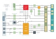
Block Diagram <strong>CD3</strong>-JIVE<br />
DVI-I<br />
Digital/Analog<br />
VGA<br />
D-SUB<br />
DVI-D<br />
Digital<br />
COM<br />
D-SUB<br />
DVI<br />
RGB<br />
VGA<br />
Option<br />
DVI<br />
RS-<br />
232<br />
RS-<br />
485<br />
USB<br />
GE<br />
Alternative CPU:<br />
• Pentium® M 745 1.8GHz<br />
• LV Pentium® M 738 1.4GHz<br />
• Celeron® M 370 1.5GHz<br />
• ULV Celeron® M 373 1.0GHz<br />
Panel<br />
Link<br />
Panel<br />
Link<br />
Option<br />
SP<br />
334<br />
82<br />
573<br />
82<br />
573<br />
SA<br />
Dual SDVO<br />
CU<br />
PCIe<br />
GE<br />
GPIO<br />
USB<br />
Pentium® M<br />
760<br />
2.0GHz<br />
SATA<br />
SATA<br />
Sheet 2<br />
PCIe<br />
PCIe<br />
FSB<br />
533MHz<br />
GMCH<br />
82915<br />
GM<br />
DMI x 4<br />
ICH6<br />
82801<br />
PATA<br />
AC '97<br />
LPC<br />
PCI<br />
DDR2 533<br />
1GB / 2GB<br />
AC '97<br />
Block Diagram<br />
<strong>CD3</strong>-JIVE<br />
Rev. 1<br />
Sheet 1/2<br />
SIO<br />
FWH<br />
BIOS<br />
IDE I/F Expansion I/F<br />
Option<br />
SO-DIMM 200<br />
SO-DIMM 200<br />
87<br />
61<br />
82<br />
802<br />
VGA<br />
USB<br />
GPIO<br />
AC '97<br />
GPIO<br />
PS/2<br />
COM<br />
PCI<br />
C10-CFA<br />
CompactFlash<br />
ATA<br />
© <strong>EKF</strong> -16- ekf.com<br />
LPC<br />
GPIO<br />
USB<br />
CompactPCI CompactPCI<br />
J4<br />
J1<br />
J2
Front Panel I/O<br />
<strong>User</strong> <strong>Guide</strong> <strong>CD3</strong>-JIVE • Advanced CompactPCI 6U Pentium® M CPU Board<br />
Block Diagram<br />
<strong>CD3</strong>-JIVE<br />
Rev. 1<br />
Sheet 2/2<br />
PCI<br />
PCIe to PCI<br />
Bridge<br />
81<br />
11<br />
PMC<br />
Mezzanine<br />
PMC Module<br />
and/or<br />
2.5-Inch SATA Hard Disk Module<br />
C14-SATA Mounts on Top of the PMC<br />
PCIe<br />
SIO<br />
GPIO14<br />
SATA<br />
SATA0/1<br />
SATA<br />
Dual 2.5-Inch HD<br />
Option<br />
C14-SATA Dual 2.5-" HD Module<br />
PCI<br />
Local Power<br />
Sheet 1<br />
PCIe<br />
GE<br />
1 2<br />
4<br />
Basic Hot Swap<br />
Controller PICMG 2.1<br />
16<br />
46<br />
82<br />
573<br />
CPCI Power<br />
GE<br />
PICMG 2.16<br />
GE<br />
SATA 0/1<br />
SATA 2/3<br />
SATA 0/1<br />
PMC<br />
Rear I/O<br />
© <strong>EKF</strong> -17- ekf.com<br />
SATA<br />
SW1<br />
J-SATA<br />
or SIO<br />
GPIO25<br />
SATA<br />
SW2<br />
CompactPCI<br />
J3<br />
CompactPCI<br />
J5
<strong>User</strong> <strong>Guide</strong> <strong>CD3</strong>-JIVE • Advanced CompactPCI 6U Pentium® M CPU Board<br />
Top View Component Assembly <strong>CD3</strong>-JIVE<br />
VGA COM<br />
RST<br />
DVI 1 DVI 2<br />
USB<br />
USB<br />
Red Outline:<br />
PMC Mezzanine Module<br />
Option<br />
GBE<br />
GBE<br />
J-SPK<br />
J-GP<br />
1<br />
J-SWAP<br />
J-RTC<br />
1<br />
P-SA<br />
GBE<br />
GBE<br />
<strong>CD3</strong>-JIVE<br />
© <strong>EKF</strong><br />
ekf.com<br />
J-COM<br />
P-IDE<br />
P-CU<br />
DDR2 SODIMM<br />
DDR2 SODIMM<br />
FWH<br />
GMCH<br />
P-SATA<br />
Programmable<br />
LEDs<br />
BAT<br />
GBE<br />
J-LRST +<br />
P-EXP<br />
0 1 2 3<br />
PCIe<br />
to<br />
PCI<br />
Yellow Outline:<br />
Dual SATA Hard Disk Drive<br />
Mezzanine Module Option<br />
C14<br />
CompactFlash ATA<br />
Module Area<br />
C10<br />
1<br />
1<br />
© <strong>EKF</strong> • <strong>CD3</strong>-JIVE • ekf.com<br />
MJ1<br />
CPU<br />
ICH6<br />
1 1<br />
© <strong>EKF</strong> -18- ekf.com<br />
MJ2<br />
1<br />
MJ4<br />
J4 J4<br />
J4 J4
<strong>User</strong> <strong>Guide</strong> <strong>CD3</strong>-JIVE • Advanced CompactPCI 6U Pentium® M CPU Board<br />
CDT-RIO Rear I/O Transition Module<br />
Short Description<br />
Available as a rear I/O expansion board to the<br />
<strong>CD3</strong>-JIVE CPU card, the CDT-RIO is provided<br />
with several I/O port connectors, to be used<br />
either in addition to the <strong>CD3</strong>-JIVE front panel<br />
connectors or alternatively. Being mainly a<br />
passive rear I/O transition module, groups of<br />
signals from the <strong>CD3</strong>-JIVE CPU board are<br />
passed across the CompactPCI J3-5/P3-5<br />
connector to the CDT-RIO. Some of the data<br />
lines are available locally on the CDT board for<br />
system internal wiring only, while other<br />
connectors such as VGA-Video and Gigabit<br />
Ethernet are mounted into the back panel for<br />
external use. USB and SATA (eSATA) channels<br />
are provided both on-board and externally.<br />
CDT-RIO Rear I/O Transition Module (Option)<br />
Typically the CDT-RIO is equipped with a 4-HP<br />
rear panel (20.3mm width). As a custom<br />
specific option, an 8-HP panel is available with<br />
additional connectors. Utilization of the CDT-<br />
RIO transition module adds a level of I/O<br />
functionality that is not available with the <strong>CD3</strong>-<br />
JIVE CPU board alone. Further on, swapping the<br />
CPU card is simplified by means of rear I/O,<br />
which is important for efficient system<br />
maintenance (MTTR).<br />
For technical details please refer to the 'CDT-RIO<br />
Technical Information Manual', available at<br />
www.ekf.com/c/ccpu/cd3/cdt_tie.pdf.<br />
© <strong>EKF</strong> -19- ekf.com
<strong>User</strong> <strong>Guide</strong> <strong>CD3</strong>-JIVE • Advanced CompactPCI 6U Pentium® M CPU Board<br />
<strong>CD3</strong>-JIVE with CDT-RIO<br />
© <strong>EKF</strong> -20- ekf.com
<strong>User</strong> <strong>Guide</strong> <strong>CD3</strong>-JIVE • Advanced CompactPCI 6U Pentium® M CPU Board<br />
Rear I/O CPCI Rear I/O CPCI<br />
Rear I/O CPCI<br />
J5<br />
<strong>CD3</strong>-JIVE<br />
Rear I/O<br />
J4<br />
<strong>CD3</strong>-JIVE<br />
Rear I/O<br />
J3<br />
PMC<br />
Rear I/O<br />
HD-Audio<br />
USB<br />
PS/2<br />
Serial<br />
ATA<br />
Assembly Drawing CDT-RIO<br />
Block Diagram CDT-RIO<br />
P-GPIO +5V<br />
P-POW<br />
Block Diagram<br />
CDT-RIO<br />
USB<br />
COM (TTL) ADM COM<br />
211 (RS-232)<br />
VGA<br />
P-SA1<br />
GPIO<br />
PS/2<br />
GPIO<br />
P-PS2<br />
10/100/1000Mbps<br />
Ethernet<br />
P-PMC<br />
PMC<br />
LM<br />
35<br />
26<br />
LM<br />
35<br />
26<br />
P-CU<br />
CU<br />
SA<br />
P-AUDIO<br />
USB4<br />
P-SA2<br />
SP0 SP1 SP2 SP3A<br />
SATA<br />
Audio<br />
SATA<br />
SA<br />
USB<br />
JMP-COM<br />
+5V<br />
SATA<br />
SATA<br />
optional<br />
mezzanine<br />
back panel<br />
adapter<br />
Mezzanine I/O<br />
Back<br />
Panel<br />
I/O<br />
USB<br />
USB<br />
USB<br />
© <strong>EKF</strong> -21- ekf.com<br />
VGA<br />
GETH<br />
GETH<br />
SATA<br />
COM<br />
VGA<br />
GE<br />
GE<br />
eSATA<br />
6U<br />
4HP
<strong>User</strong> <strong>Guide</strong> <strong>CD3</strong>-JIVE • Advanced CompactPCI 6U Pentium® M CPU Board<br />
J4 J4<br />
2<br />
1<br />
P-PMC<br />
P-GPIO<br />
CDT-RIO<br />
© <strong>EKF</strong><br />
ekf.com<br />
SATA<br />
1<br />
1<br />
1<br />
1<br />
1<br />
P-POW<br />
reserved area for mezzanine module<br />
SP2 SP1 SP0<br />
P-AUDIO<br />
1<br />
P-CU<br />
reserved area for on-board USB stick<br />
1<br />
USB4<br />
1<br />
1<br />
1<br />
P-SA2<br />
P-SA1<br />
P-PS2<br />
SATA<br />
1<br />
JMP-COM2<br />
SP3A<br />
2 8<br />
7<br />
1<br />
2 8<br />
7<br />
1<br />
USB2 USB3<br />
USB1<br />
COM<br />
VGA<br />
ETH3 ETH2<br />
SP3<br />
eSATA<br />
1 1<br />
SATA_GPIO_LED<br />
© <strong>EKF</strong> • CDT-RIO • ekf.com<br />
© <strong>EKF</strong> -22- ekf.com<br />
LED
<strong>User</strong> <strong>Guide</strong> <strong>CD3</strong>-JIVE • Advanced CompactPCI 6U Pentium® M CPU Board<br />
<strong>CD3</strong>-JIVE On-Board Elements<br />
Strapping Headers<br />
ISPCON PLD programming connector, not stuffed<br />
J-GP Jumper to reset BIOS CMOS RAM values<br />
J-LRST Jumper to reset Board<br />
J-RTC Jumper to reset RTC core of ICH6, not stuffed<br />
J-SPK Speaker connector<br />
JSWAP Hot Swap Micro Switch Connector<br />
JSATA SATA switch CPCI J3/J5, not stuffed<br />
Connectors & Sockets<br />
J1/J2 CompactPCI Bus 32-bit, 33MHz, PXI Trigger<br />
J3/J4/J5 CompactPCI Rear I/O<br />
MJ1/2/4 PMC mezzanine module connectors, 32-bit PCI, rear I/O option<br />
P-CU UART COM port (TTL level) pin header provided for an optional <strong>EKF</strong><br />
CU-series PHY module<br />
P-EXPT<br />
P-EXPB<br />
P-IDET<br />
P-IDEB<br />
Expansion interface connector for optional mezzanine companion<br />
boards such as CCA-LAMBADA or CCB-BOSSANOVA, available either<br />
from top (T) or bottom (B) of the <strong>CD3</strong>-JIVE board<br />
Ultra ATA/100 IDE port, either for C10-CFA mezzanine module with<br />
CompactFlash Card or 1.8-Inch ATA hard disk, or optional mezzanine<br />
companion boards such as CCA-LAMBADA or CCB-BOSSANOVA,<br />
available either from top (T) or bottom (B) of the <strong>CD3</strong>-JIVE board<br />
P-ITP CPU debug port<br />
P-SA UART COM port (TTL level) connector provided for an optional MEN<br />
SA-type PHY mezzanine module<br />
P-SATA Serial ATA mezzanine module connector, provided for the C14-SATA<br />
dual hard disk option<br />
SODIMM1<br />
SODIMM2<br />
LED Indicators<br />
200-pin DDR2 memory module SDRAM PC2-3200/4200 (DDR400/533)<br />
sockets<br />
LED0 ... 3 <strong>User</strong> programmable LEDs (option)<br />
© <strong>EKF</strong> -23- ekf.com
<strong>User</strong> <strong>Guide</strong> <strong>CD3</strong>-JIVE • Advanced CompactPCI 6U Pentium® M CPU Board<br />
<strong>CD3</strong>-JIVE Front Panel Elements<br />
GBE 1<br />
GBE 2<br />
1000Base-TX/100Base-TX/10Base-T, RJ-45 receptacles with<br />
integrated indicator LEDs activity & speed<br />
USB1/2 Universal Serial Bus 2.0 self powered root hub, type A receptacle<br />
DVI 1<br />
VGA<br />
DVI 2<br />
COM<br />
DVI-I integrated (digital & analog) receptacle, suitable for DVI<br />
digital flat panel displays and/or analog monitors<br />
Option VGA D-Sub connector<br />
DVI-D (digital-only) receptacle, suitable for DVI digital flat panel<br />
displays<br />
Option CU/SA-type mezzanine module or COM port connector<br />
PMC PMC mezzanine module front panel connector(s)<br />
GP General Purpose LED<br />
HD LED indicating any activity on IDE or SATA ports<br />
HS Hot swap LED (Blue)<br />
ETH3 Activity LED rear panel (or PICMG 2.16 backplane) GBE port<br />
Reset<br />
(PWR/RES)<br />
Reset push-button switch with integrated indicator LED (power<br />
good)<br />
© <strong>EKF</strong> -24- ekf.com
Microprocessor<br />
<strong>User</strong> <strong>Guide</strong> <strong>CD3</strong>-JIVE • Advanced CompactPCI 6U Pentium® M CPU Board<br />
The <strong>CD3</strong>-JIVE is designed for use with Pentium® M and Celeron® M processors manufactured in<br />
90nm technology (Dothan). These include also the Ultra Low-Voltage (ULV) Celeron® M and the Low-<br />
Voltage (LV) Pentium® M processors as listed below. The processors are housed in a Micro FC-BGA<br />
package for direct soldering to the PCB, i.e. the CPU chip cannot be removed or changed by the user.<br />
The processors supported by the <strong>CD3</strong>-JIVE are running at FSB clock speeds of 400MHz and 533MHz.<br />
The internal Pentium M processor speed is achieved by multiplying the host bus frequency by a<br />
variable value. The multiplier is chosen by currently required performance and the actual core<br />
temperature. This technology is called Enhanced Intel SpeedStep®.<br />
Power is applied across the CompactPCI connectors J1 (3.3V, 5V). The processor core voltage is<br />
generated by a switched voltage regulator, sourced from the 5V plane. The processor signals its<br />
required core voltage by 6 dedicated pins according to Intels IMVP-IV voltage regulator specification.<br />
Processor Speed<br />
min/max<br />
[GHz]<br />
ULV Celeron M 373<br />
1) 2)<br />
LV Pentium M 738 2)<br />
Pentium M 745 2)<br />
Pentium M 760 2)<br />
90nm (Dothan) Processors Supported<br />
Host Bus<br />
[MHz]<br />
L2 Cache<br />
[MB]<br />
TDP<br />
[W]<br />
Die Temp<br />
[°C]<br />
CPU ID Stepping sSpec<br />
1.0/1.0 400 0.5 5 0-100 06D8h C-0 SL8LW<br />
0.6/1.4 400 2 10 0-100 06D6h<br />
06D8h<br />
0.6/1.8 400 2 21 0-100 06D6h<br />
06D8h<br />
B-1<br />
C-0<br />
B-0<br />
C-0<br />
SL7P9<br />
SL89N<br />
SL7Q6<br />
SL8U8<br />
0.8/2.0 533 2 27 0-100 06D8h C-0 SL869<br />
1)<br />
This processor does not support SpeedStep® technology, thus it runs at a fixed core speed.<br />
2)<br />
Following the Intel Embedded Roadmap, this processor is recommended for long time availability.<br />
© <strong>EKF</strong> -25- ekf.com
<strong>User</strong> <strong>Guide</strong> <strong>CD3</strong>-JIVE • Advanced CompactPCI 6U Pentium® M CPU Board<br />
Thermal Considerations<br />
In order to avoid malfunctioning of the <strong>CD3</strong>-JIVE, take care of appropriate cooling of the processor<br />
and system, e.g. by a cooling fan suitable to the maximum power consumption of the CPU chip<br />
actually in use. Please note, that the processors temperature is steadily measured by a special<br />
controller (LM87), attached to the onboard SMBus ® (System Management Bus). A second<br />
temperature sensor internal to the LM87 allows for acquisition of the boards surface temperature.<br />
Beside this the LM87 also monitors most of the supply voltages. A suitable software to display both,<br />
the temperatures as well as the supply voltages, is MBM (Motherboard Monitor), which can be<br />
downloaded from the web. After installation, both temperatures and voltages can be observed<br />
permanently from the Windows taskbar.<br />
The <strong>CD3</strong>-JIVE is equipped with a passive heatsink. Its height takes into account the 4HP limitation in<br />
mounting space of a CPCI board. In addition, a forced vertical airflow through the system enclosure<br />
(e.g. bottom mount fan unit) is strongly recommended (>15m 3 /h or 200LFM around the CPU slot).<br />
As an exception, the <strong>CD3</strong>-2-JIVE (ULV Celeron M 1GHz) can be operated with natural convection only.<br />
Be sure to thoroughly discuss your actual cooling needs with <strong>EKF</strong>. Generally, the faster the CPU speed<br />
the higher its power consumption. For higher ambient temperatures, consider increasing the forced<br />
airflow to 400 or 600LFM.<br />
The table showing the supported processors above give also the maximum power consumption (TDP<br />
= Thermal Design Power) of a particular processor. Fortunately, the power consumption is by far<br />
lower when executing typical Windows or Linux tasks. The heat dissipation increases when e.g.<br />
rendering software like the Acrobat Distiller is executed.<br />
The Pentium M processors support Intel's Enhanced SpeedStep® technology. This enables dynamic<br />
switching between multiple core voltages and frequencies depending on core temperature and<br />
currently required performance. The processors are able to reduce their core speed and core voltage<br />
in up to 8 steps down to 600MHz. This leads to an obvious reduction of power consumption (max.<br />
7.5W @600MHz) resulting in less heating. This mode of lowering the processor core temperature is<br />
called TM2 (TM=Thermal Monitor). Note, that TM2 is not supported by Celeron M processors.<br />
Another way to reduce power consumption is to modulate the processor clock. This mode (TM1) is<br />
supported also by the Celeron M processors and is achieved by actuating the 'Stop Clock' input of the<br />
CPU. A throttling of 50% e.g. means a duty cycle of 50% on the stop clock input. However, while<br />
saving considerable power consumption, the data throughput of the processor is also reduced. The<br />
processor works at full speed until the core temperature reaches a critical value. Then the processor<br />
is throttled by 50%. As soon as the high temperature situation disappears the throttling will be<br />
disabled and the processors runs at full speed again.<br />
A similar feature is embedded within the Graphics and Memory Controller (GMCH) i915GM. An ondie<br />
temperature sensor is used to protect the GMCH from exceeding its maximum junction<br />
temperature (T J,max=105°C) by reducing the memory bandwidth.<br />
These features are controllable by BIOS menu entries. By default the BIOS of the <strong>CD3</strong>-JIVE enables<br />
mode TM2 which is the most efficient.<br />
Main Memory<br />
The <strong>CD3</strong>-JIVE is equipped with two sockets for installing 200-pin SO-DIMM modules (module height<br />
= 1.25 inch). Supported are unbuffered DDR2 SO-DIMMs (V CC=1.8V) without ECC featuring on-die<br />
© <strong>EKF</strong> -26- ekf.com
<strong>User</strong> <strong>Guide</strong> <strong>CD3</strong>-JIVE • Advanced CompactPCI 6U Pentium® M CPU Board<br />
termination (ODT), according the PC2-3200 or PC2-4200 specification. Minimum memory size is<br />
128MB; maximum memory size is 2GB. Due to the video requirements of the i915GM chipset, a<br />
minimum of 2x256MB of memory is recommended for the operating systems Windows NT 4.0,<br />
Windows 2000 or Windows XP (some of the system memory is dedicated to the graphics controller).<br />
The contents of the SPD EEPROM on the SO-DIMMs is used by the BIOS at POST (Power-on Self Test)<br />
to program the memory controller within the chipset.<br />
The i915GM chipset supports symmetric and asymmetric memory organization. The maximum<br />
memory performance can be obtained by using the symmetric mode. To achieve this mode two SO-<br />
DIMMs of equal capacity must be installed in the memory sockets. In asymmetric mode different<br />
memory modules may be used with the drawback of less bandwidth. A special case of asymmetric<br />
mode is to populate only one memory module (i.e. one socket may be left empty).<br />
LAN Subsystem<br />
The Ethernet LAN subsystem is composed of three Intel 82573 Gigabit Ethernet controllers that<br />
provide also legacy 10Base-T and 100Base-TX connectivity. Two Ethernet ports are fed to two RJ45<br />
jacks located in the front panel (one is configurable as an alternative to backplane packet switching<br />
according PICMG Spec 2.16, or CDT-RIO rear panel I/O). The third Ethernet controller is solely available<br />
for backplane packet switching or rear panel I/O. Each port includes the following features:<br />
< One PCI Express lane per Ethernet controller (250MB/s)<br />
< 1000Base-Tx (Gigabit Ethernet), 100Base-TX (Fast Ethernet) and 10Base-T capability<br />
< Half- or full-duplex operation<br />
< IEEE 802.3 Auto-Negotiation for the fastest available connection<br />
< Jumperless configuration (complete software-configurable)<br />
< Two bicoloured LEDs integrated into the dedicated RJ-45 connectors to signal the LAN link, the<br />
LAN connection speed, and activity status.<br />
Each NIC (Networking Interface Controller) is connected by a single PCI Express lane to the chipset<br />
(ICH6). Their MAC addresses (unique hardware numbers) are stored in dedicated EEPROMs. The Intel<br />
Ethernet software and drivers for the 82573 is available from Intel's website for download.<br />
© <strong>EKF</strong> -27- ekf.com
<strong>User</strong> <strong>Guide</strong> <strong>CD3</strong>-JIVE • Advanced CompactPCI 6U Pentium® M CPU Board<br />
Serial ATA Interface (SATA)<br />
The <strong>CD3</strong>-JIVE provides four serial ATA (SATA) ports, each capable of transferring 150MB/s. Integrated<br />
within the ICH6, the SATA controller features different modes to support also legacy operating<br />
systems.. The four SATA channels are routed to the CompactPCI J3 connector, thus they are accessible<br />
via the rear I/O transition module CDT-RIO.<br />
Two serial ATA ports could be switched alternately to an onboard connector suitable for mounting<br />
C14-SATA. The other two SATA channels could be switched between CompactPCI J3 an CompactPCI<br />
J5<br />
A LED named HD located in the front panel, signals disk activity status of the SATA and IDE devices.<br />
Available for download from Intel's web site are drivers for popular operating systems, e.g. Windows®<br />
2000, Windows® XP and Linux.<br />
Enhanced IDE Interface<br />
The EIDE interface handles the exchange of information between the processor and legacy mass<br />
storage peripheral devices like hard disks, ATA CompactFlash cards and CD-ROM drives. The interface<br />
supports:<br />
< Up to two parallel ATA devices<br />
< PIO Mode 3/4, Ultra ATA/33, Ultra ATA/66, Ultra ATA/100<br />
The IDE interface is routed to the on-board connectors P-IDET and P-IDEB (T:top side, B:bottom side<br />
of the board). P-IDE is used to interface to the CompactFlash Card adapter C10-CFA or to the<br />
expansion board CCA-LAMBADA. Use the C10-CFA adapter to attach a CompactFlash ATA style silicon<br />
disk, whenever a hard disk is not suitable for your system, or as an additional mass storage device. The<br />
CCA-LAMBADA expansion board is capable to carry an on-board 1.8" or 2.5" hard disk drive. When<br />
using the 1.8" option the concurrent operation of a CompactFlash device is possible.<br />
A LED named HD located in the front panel signals the disk activity status of both the IDE and SATA<br />
devices.<br />
The IDE controller is integrated into the ICH6. Ultra ATA IDE drivers can be downloaded from the Intel<br />
web site.<br />
© <strong>EKF</strong> -28- ekf.com
Graphics Subsystem<br />
<strong>User</strong> <strong>Guide</strong> <strong>CD3</strong>-JIVE • Advanced CompactPCI 6U Pentium® M CPU Board<br />
The graphics subsystem is part of the Intel i915GM Graphics/Memory Controller Hub (GMCH) and<br />
supports dual screen operation. The <strong>CD3</strong>-JIVE therefore is provided with a DVI-I (DVI 1) and in<br />
addition a DVI-D (DVI 2) graphics connector. DVI-I is both a digital and analog interface, DVI-D is only<br />
a digital interface. Recent digital input flat-panel displays are widely available with this connector style.<br />
For classic monitors, adapters or adapter cables can be used for converting from DVI-I to the 15-pin<br />
HD D-SUB connector.<br />
A special display transmitter chip is used to convert Intel's proprietary, PCI express based SDVO<br />
interface to the differential DVI signals. The SiI1362 (Silicon Image) transmitter uses PanelLink® Digital<br />
technology to support displays ranging from VGA to UXGA resolutions (25 - 165Mpps) in a single link<br />
interface.<br />
The GMCH supports several video resolutions and refresh rates. A partial list is contained in the table<br />
below. Please note, that flat-panel displays should be operated with their maximum resolution at<br />
60Hz refresh rate.<br />
Partial List of i915GM GMCH Video Modes (analog / digital)<br />
Resolution 60Hz 70Hz 72Hz 75Hz 85Hz<br />
640x480 T / T T / T T / T T / T T / T<br />
800x600 T / T T / T T / T T / T T / T<br />
1024x768 T / T 1)<br />
1280x1024 T / T 1)<br />
1600x1200 T / T 1)<br />
T / T T / T T / T T / T<br />
T / T T / T T / T T / T<br />
T / - T / - T / - T / -<br />
2048x1536 T / - T / - T / - T / - - / -<br />
1) This video mode is suitable for popular flat-panel displays.<br />
As an alternative option to the DVI 1 receptacle, the <strong>CD3</strong>-JIVE can be equipped with an ordinary HD<br />
D-Sub 15-lead connector (VGA style). This connector is suitable for analog signals only, so the<br />
PanelLink transmitter is not stuffed with this option. Nevertheless also flat-panel displays can be<br />
attached to the D-Sub connector but with minor reduced image quality.<br />
Independent from the video connector actually in use, DVI or VGA, the VESA DDC 2B standard is<br />
supported. This is a two-wire serial bus (clock, data), which is controlled by the GMCH and allows to<br />
read out important parameters, e.g. the maximum allowable resolution, from the attached monitor.<br />
In addition, DDC Power (+5V) is delivered to either connector. A resettable fuse is stuffed to protect<br />
the board from an external short-circuit condition (0.75A).<br />
Graphics drivers for the i915GM can be downloaded from the Intel web site.<br />
© <strong>EKF</strong> -29- ekf.com
Real-Time Clock<br />
<strong>User</strong> <strong>Guide</strong> <strong>CD3</strong>-JIVE • Advanced CompactPCI 6U Pentium® M CPU Board<br />
The <strong>CD3</strong>-JIVE has a time-of-day clock and 100-year calendar, integrated into the ICH6. A battery on<br />
the board keeps the clock current when the computer is turned off. The <strong>CD3</strong> uses a BR2032 lithium<br />
battery soldered in the board, giving an autonomy of more than 3 years. Under normal conditions,<br />
replacement should be superfluous during lifetime of the board.<br />
Universal Serial Bus (USB)<br />
The <strong>CD3</strong>-JIVE is provided with eight USB ports, all of them are USB 2.0 capable. Two USB interfaces<br />
are routed to front panel connectors, two ports are feed to the expansion board interface connectors<br />
P-EXP, and four ports are optionally available for rear I/O across the J4/P4 CompactPCI connector.<br />
The front panel USB connectors can source up to 0.5A/5V each, over-current protected by two<br />
electronic switches. Protection for the USB ports on the expansion interface and on the rear I/O<br />
connector is located on the CCA-LAMBADA and the CDT-RIO respective. The USB controllers are<br />
integrated into the ICH6.<br />
LPC Super-I/O Interface<br />
In a modern system, legacy ports as PS/2 keyboard/mouse, COM1/2 and LPT have been replaced by<br />
USB and Ethernet connectivity. The 1.4MB floppy disk drive has been swapped against CD-RW drives,<br />
attached to a SATA connector, or USB memory sticks. Hence, the <strong>CD3</strong>-JIVE is virtually provided with<br />
all necessary I/O ports. However, for compatibility purposes the <strong>CD3</strong>-JIVE is additionally equipped with<br />
a simple Super-I/O chip, for optional rear I/O of PS/2 keyboard/mouse and COM1 (TTL level only)<br />
across the J4/P4 CPCI connector. COM1 is also available as front panel connector option, if the DVI 2<br />
video connector would not be needed (requires a SA-type PHY module attached to P-SA). The Super-<br />
I/O controller resides on the local LPC bus (LPC = Low Pin Count interface standard), which is a<br />
serialized ISA bus replacement.<br />
As an alternative, <strong>EKF</strong> offers the CCA-LAMBADA or CCB-BOSSANOVA mezzanine expansion modules<br />
to the <strong>CD3</strong>-JIVE, featuring all classic Super-I/O functionality. The CCA-LAMBADA is a 3U Eurocard with<br />
a 4HP (single) width front panel. Access to the connectors PS/2 (mouse, keyboard), COM, USB and<br />
audio in/out is given directly from the front panel. The CCA-LAMBADA connects to the <strong>CD3</strong>-JIVE<br />
across the connector P-EXPT or P-EXPB, hence the CCA-LAMBADA can be attached either to the top<br />
or to the bottom of the <strong>CD3</strong>-JIVE.<br />
© <strong>EKF</strong> -30- ekf.com
Reset/Watchdog<br />
<strong>User</strong> <strong>Guide</strong> <strong>CD3</strong>-JIVE • Advanced CompactPCI 6U Pentium® M CPU Board<br />
The <strong>CD3</strong>-JIVE is provided with two supervisor circuits to monitor the supply voltages 1.8V, 3.3V, 5V,<br />
and to generate a clean power-on reset signal.<br />
The reset manual push-button is situated at the front panel. The button is indent mounted behind the<br />
front and requires a tool, e.g. pen to be pressed, preventing from being inadvertently activated. The<br />
push button reset signal is routed across a PLD (programmable logic device) and could be inhibited on<br />
customers request.<br />
An alternative way to generate a system reset is to activate the signal PRST# located on CompactPCI<br />
connector J2 pin C17. Pulling this signal to GND will have the same effect as to push the handle's red<br />
push button.<br />
The healthy state of the <strong>CD3</strong>-JIVE is signalled by the LED PG (Power Good) located in the front panel.<br />
As soon as this LED begins to shine all power voltages are within their specifications and the reset<br />
signal has been deasserted.<br />
An important reliability feature is the watchdog function, which is programmable by software. The<br />
behaviour of the watchdog is defined within the PLD, which activates/deactivates the watchdog and<br />
controls its time-out period. The time-out delay is adjustable in the steps 2, 10, 50 and 255 seconds.<br />
After alerting the WD and programming the time-out value, the related software (e.g. application<br />
program) must trigger the watchdog periodically. All watchdog related functions are made available<br />
by calling service requests within the BIOS.<br />
The watchdog is in a passive state after a system reset. There is no need to trigger it at boot time. The<br />
watchdog is activated on the first trigger request. If the duration between two trigger requests<br />
exceeds the programmed period, the watchdog times out and a system reset will be generated. The<br />
watchdog remains in the active state until the next system reset. There is no way to disable it once it<br />
had been put on alert, whereas it is possible to reprogram its time-out value at any time.<br />
Firmware Hub (Flash BIOS)<br />
The BIOS is stored in an 82802 8Mbit Firmware Hub (there are second sources in use with deviant<br />
part numbers). The firmware hub contains a nonvolatile memory core based on flash technology,<br />
allowing the BIOS to be upgraded.<br />
The FWH can be reprogrammed (if suitable) by a DOS based tool. This program and the latest <strong>CD3</strong>-<br />
JIVE BIOS are available from the <strong>EKF</strong> website. Read carefully the enclosed instructions. If the<br />
programming procedure fails e.g. caused by a power interruption, the <strong>CD3</strong>-JIVE may no more be<br />
operable. In this case you would have to send in the board, because the BIOS is directly soldered to<br />
the PCB and cannot be changed by the user.<br />
© <strong>EKF</strong> -31- ekf.com
Mezzanine Interfaces<br />
<strong>User</strong> <strong>Guide</strong> <strong>CD3</strong>-JIVE • Advanced CompactPCI 6U Pentium® M CPU Board<br />
The PMC mezzanine card socket enables on-board expansion of the <strong>CD3</strong>-JIVE.<br />
The PMC slot on the <strong>CD3</strong> supports a 32-bit/66MHz PCI interface with VI/O=3.3V. The modules rear<br />
I/O is wired to the CompactPCI connector J5. Alternatively I/O can be obtained via the front panel<br />
connector of the module (if any).<br />
As an option, the <strong>CD3</strong>-JIVE is also available with a dual 2.5-inch SATA hard disk add-on module<br />
(C14-SATA), which occupies the PMC slot.<br />
PG (Power Good) LED<br />
The <strong>CD3</strong>-JIVE offers a software programmable LED located in the reset push-button. After system<br />
reset, this LED defaults to signal the board healthy respective power good state. This LED changes its<br />
function by calling an appropriate BIOS request and is then controlled by software only. The PG LED<br />
remains in the programmable state until the next system reset occurs.<br />
HD (Hard Disk Activity) LED<br />
The <strong>CD3</strong>-JIVE offers a LED, marked as HD (placed within the front panel). This LED signals activity on<br />
any device attached to the SATA or the IDE ports.<br />
GP (General Purpose) LED<br />
A second, programmable LED can be also observed from the front panel. The status of the GP LED is<br />
controlled by the GPO18 output of the ICH6. Setting this pin to 1 will switch on the LED. As of<br />
current, the GP LED is not dedicated to any particular hardware or firmware function (this may change<br />
in the future).<br />
Hot Swap Detection<br />
The <strong>CD3</strong>-JIVE uses a LTC1646 hot swap power controller. The main task of this device is a controlled<br />
switching of the board power supplies. On-board insertion the various power planes on the board<br />
(3.3V, 5V, ±12V) are ramped up slowly to avoid too large voltage drops within the system. When all<br />
voltages have reached their nominal values the controller asserts the CompactPCI signal HEALTHY#<br />
(connector J1 pin B4). Electronic circuit breakers protect +3.3V and +5V against overcurrent fault<br />
conditions. As soon as the current on these supplies exceed a value of 11A, the power of all supplies<br />
(including ±12V) are switched off and the fault is flagged to the system by deasserting the<br />
HEALTHY# signal.<br />
The CompactPCI specification added the signal ENUM# to the PCI bus to allow the system hot<br />
swapping. This signal is routed to the GPI3 of the ICH6 on the <strong>CD3</strong>-JIVE. A System Management<br />
Interrupt (SMI) can be requested if ENUM# changes by insertion or removal of a board.<br />
Blue Hot Swap LED<br />
The <strong>CD3</strong>-JIVE is equipped with a blue LED (a LED marked as HS is placed in the front panel near the<br />
lower board handle), that indicates when board extraction is permitted. A micro switch in one of the<br />
front panel ejectors signals when a board extraction event takes place. This micro switch is connected<br />
via the 3-pin header JSWAP.<br />
© <strong>EKF</strong> -32- ekf.com
<strong>User</strong> <strong>Guide</strong> <strong>CD3</strong>-JIVE • Advanced CompactPCI 6U Pentium® M CPU Board<br />
Power Supply Status (DEG#, FAL#)<br />
Power supply failures may be detected before the system crashes down by monitoring the signals<br />
DEG# or FAL#. These active low lines are additions of the CompactPCI specification and may be<br />
driven by the power supply. DEG# signals the degrading of the supply voltages, FAL# there possible<br />
failure. On the <strong>CD3</strong>-JIVE the signal FAL# is routed to the GPI4 and DEG# to the GPI5 of the ICH6.<br />
PXI Trigger Signals<br />
As a stuffing option (resistor network), the <strong>CD3</strong>-JIVE supports four of the eight trigger signals of the<br />
PXI standard across the connector J2, as defined by National Instruments. The trigger signals are<br />
provided by the local SIO (Super-I/O) chip IT8761E. GPIO20/21 are routed to TRIG0/1, and GPIO26/27<br />
are used to control TRIG6/7. These signals may alternatively be used as GPIO lines in a non-PXI<br />
environment.<br />
GPIO Signals<br />
As an alternative, the IT8761E GPIO20/21 and GPIO26/27 are also available from the rear I/O<br />
connector J4 (stuffing option by means of a resistor network). In addition, the IT8761E GPIO22 ..<br />
GPIO24 are permanently wired to J4. GPIO25 is (default) used for switching SATA signals between<br />
CompactPCI J3 and CompactPCI J5. As a stuffing option GPIO25 could be wired to J4.<br />
In addition to the GPIO lines listed above available for rear I/O on J2 and/or J4, the expansion<br />
connector P-EXP provides another two GPIO lines available for user specific application. The 5V TTL<br />
signals sio_gpio16/17 are controlled by the on-board SIO IT8761E, with an internal 50kΩ PU resistor<br />
and capable of sinking 24mA each.<br />
© <strong>EKF</strong> -33- ekf.com
Rear I/O Options<br />
<strong>User</strong> <strong>Guide</strong> <strong>CD3</strong>-JIVE • Advanced CompactPCI 6U Pentium® M CPU Board<br />
Optionally, the <strong>CD3</strong>-JIVE can be used for rear I/O with respect to the following functions:<br />
< 2 x Gigabit Ethernet - J3<br />
< 4 x SATA (up to 4 x SATA, 1 x eSATA) - J3<br />
< Analog video (VGA) - J4<br />
< 4 x USB - J4<br />
< PS/2 keyboard & mouse - J4<br />
< COM1 (TTL level) - J4<br />
< GPIO - J4<br />
< PMC mezzanine module rear I/O - J5<br />
The analog graphics and the Gigabit Ethernet port 1 lines are routed to signal multiplexers on the<br />
<strong>CD3</strong>-JIVE. These analog signal switches, controlled by the BIOS, select either the front panel or the<br />
rear I/O connection. This is also true for the SATA channels 0/1, which can either be used for an onboard<br />
SATA hard disk mezzanine module (C14-SATA) on the <strong>CD3</strong>-JIVE, or are externally available<br />
across J3. SATA channels 2/3 are also controlled by the BIOS, select either to be used externally on<br />
CompactPCI J3, or CompactPCI J5.<br />
The COM1 port does not include the physical transceiver (TTL level only). This transceiver is located on<br />
the rear I/O module CDT-RIO instead. If COM1 is already in use on the <strong>CD3</strong>-JIVE by means of a PHY<br />
attached to P-CU or P-SA, the transceiver on the CDT-RIO must be inhibited by removing the CDT<br />
J-COM jumper.<br />
Rear I/O is restricted to the J3 ... J5 connectors (except PXI across J2), hence the <strong>CD3</strong>-JIVE CPU card by<br />
default is suitable for any common 32/64-bit CompactPCI J1/J2 backplane.<br />
© <strong>EKF</strong> -34- ekf.com
<strong>User</strong> <strong>Guide</strong> <strong>CD3</strong>-JIVE • Advanced CompactPCI 6U Pentium® M CPU Board<br />
Installing and Replacing Components<br />
Before You Begin<br />
Warnings<br />
The procedures in this chapter assume familiarity with the general terminology associated with<br />
industrial electronics and with safety practices and regulatory compliance required for using and<br />
modifying electronic equipment. Disconnect the system from its power source and from<br />
any telecommunication links, networks or modems before performing any of the<br />
procedures described in this chapter. Failure to disconnect power, or telecommunication<br />
links before you open the system or perform any procedures can result in personal injury<br />
or equipment damage. Some parts of the system can continue to operate even though<br />
the power switch is in its off state.<br />
Caution<br />
Electrostatic discharge (ESD) can damage components. Perform the procedures described in this<br />
chapter only at an ESD workstation. If such a station is not available, you can provide<br />
some ESD protection by wearing an antistatic wrist strap and attaching it to a<br />
metal part of the system chassis or board front panel. Store the board only in its<br />
original ESD protected packaging. Retain the original packaging (antistatic bag and<br />
antistatic box) in case of returning the board to <strong>EKF</strong> for rapair.<br />
© <strong>EKF</strong> -35- ekf.com
Installing the Board<br />
Warning<br />
<strong>User</strong> <strong>Guide</strong> <strong>CD3</strong>-JIVE • Advanced CompactPCI 6U Pentium® M CPU Board<br />
This procedure should be done only by qualified technical personnel. Disconnect the system from its<br />
power source before doing the procedures described here. Failure to disconnect power, or<br />
telecommunication links before you open the system or perform any procedures can result in personal<br />
injury or equipment damage.<br />
Typically you will perform the following steps:<br />
C Switch off the system, remove the AC power cord<br />
C Attach your antistatic wrist strap to a metallic part of the system<br />
C Remove the board packaging, be sure to touch the board only at the front panel<br />
C Identify the related CompactPCI slot (peripheral slot for I/O boards, system slot for CPU boards,<br />
with the system slot typically most right or most left to the backplane)<br />
C Insert card carefully (be sure not to damage components mounted on the bottom side of the<br />
board by scratching neighboured front panels)<br />
C A card with onboard connectors requires attachment of associated cabling now<br />
C Lock the ejector lever, fix screws at the front panel (top/bottom)<br />
C Retain original packaging in case of return<br />
© <strong>EKF</strong> -36- ekf.com
Removing the Board<br />
Warning<br />
<strong>User</strong> <strong>Guide</strong> <strong>CD3</strong>-JIVE • Advanced CompactPCI 6U Pentium® M CPU Board<br />
This procedure should be done only by qualified technical personnel. Disconnect the system from its<br />
power source before doing the procedures described here. Failure to disconnect power, or<br />
telecommunication links before you open the system or perform any procedures can result in personal<br />
injury or equipment damage.<br />
Typically you will perform the following steps:<br />
C Switch off the system, remove the AC power cord<br />
C Attach your antistatic wrist strap to a metallic part of the system<br />
C Identify the board, be sure to touch the board only at the front panel<br />
C unfasten both front panel screws (top/bottom), unlock the ejector lever<br />
C Remove any onboard cabling assembly<br />
C Activate the ejector lever<br />
C Remove the card carefully (be sure not to damage components mounted on the bottom side<br />
of the board by scratching neighboured front panels)<br />
C Store board in the original packaging, do not touch any components, hold the board at the<br />
front panel only<br />
Warning<br />
Do not expose the card to fire. Battery cells and other components could explode<br />
and cause personal injury.<br />
© <strong>EKF</strong> -37- ekf.com
<strong>User</strong> <strong>Guide</strong> <strong>CD3</strong>-JIVE • Advanced CompactPCI 6U Pentium® M CPU Board<br />
EMC Recommendations<br />
In order to comply with the CE regulations for EMC, it is mandatory to observe the following rules:<br />
C The chassis or rack including other boards in use must comply entirely with CE<br />
C Close all board slots not in use with a blind front panel<br />
C Front panels must be fastened by built-in screws<br />
C Cover any unused front panel mounted connector with a shielding cap<br />
C External communications cable assemblies must be shielded (shield connected only at one end<br />
of the cable)<br />
C Use ferrite beads for cabling wherever appropriate<br />
C Some connectors may require additional isolating parts<br />
Reccomended Accessories<br />
Blind CPCI Front<br />
Panels<br />
Ferrit Bead Filters ARP Datacom,<br />
63115 Dietzenbach<br />
Metal Shielding<br />
Caps<br />
<strong>EKF</strong> Elektronik Widths currently available<br />
(1HP=5.08mm):<br />
with handle 4HP/8HP<br />
without handle<br />
2HP/4HP/8HP/10HP/12HP<br />
Conec-Polytronic,<br />
59557 Lippstadt<br />
Ordering No.<br />
102 820 (cable diameter 6.5mm)<br />
102 821 (cable diameter 10.0mm)<br />
102 822 (cable diameter 13.0mm)<br />
Ordering No.<br />
CDFA 09 165 X 13129 X (DB9)<br />
CDSFA 15 165 X 12979 X (DB15)<br />
CDSFA 25 165 X 12989 X (DB25)<br />
© <strong>EKF</strong> -38- ekf.com
<strong>User</strong> <strong>Guide</strong> <strong>CD3</strong>-JIVE • Advanced CompactPCI 6U Pentium® M CPU Board<br />
Installing or Replacing the Memory Modules<br />
Note: If you decide to replace the memory, observe the precautions in 'Before You Begin'<br />
By default, the <strong>CD3</strong>-JIVE comes fully equipped and tested with two DDR2 SD-RAM memory modules.<br />
So normally there should be no need to install the memory modules.<br />
The <strong>CD3</strong>-JIVE requires at least one PC2-3200/4200 (400/533MHz) DDR2 SDRAM SO-DIMM module,<br />
for better performance two SO-DIMMs of equal capacity are recommended. Further it is highly<br />
recommended that Serial Presence Detect (SPD) SO-DIMMs be used, since this allows the chipset to<br />
accurately configure the memory settings for optimum performance.<br />
A replacement memory module must match the 200-pin SO-DIMM form factor (known from<br />
Notebook PCs), DDR2, V CC=1.8V, PC2-3200/PC2-4200 (400/533MHz), on-die termination (ODT),<br />
unbuffered, non-ECC style. Suitable modules are available up to 1GB. The i915GM supports modules<br />
of up to a maximum of 14 address lines (A0...A13). Memory modules organized by more than14<br />
address lines are not suitable.<br />
Replacement of the Battery<br />
When your system is turned off, a battery maintains the voltage to run the time-of-day clock and to<br />
keep the values in the CMOS RAM. The battery should last during the lifetime of the <strong>CD3</strong>-JIVE. For<br />
replacement, the old battery must be desoldered, and the new one soldered. It is recommended that<br />
you send back the board to <strong>EKF</strong> for battery replacement.<br />
Warning<br />
Danger of explosion if the battery is incorrectly replaced. Replace only with the same or<br />
equivalent type. Do not expose a battery to fire.<br />
© <strong>EKF</strong> -39- ekf.com
Technical Reference<br />
Local PCI Devices<br />
<strong>User</strong> <strong>Guide</strong> <strong>CD3</strong>-JIVE • Advanced CompactPCI 6U Pentium® M CPU Board<br />
The following table shows the on-board PCI devices and their location within the PCI configuration<br />
space. These devices consist of the Ethernet controllers and several devices within the i915GM chip<br />
set.<br />
1)<br />
2)<br />
Bus<br />
Number<br />
Device<br />
Number<br />
Function<br />
Number<br />
Vendor ID Device ID Description<br />
0 0 0 0x8086 0x2590 Host Bridge<br />
0 2 0 0x8086 0x2592 Internal Graphics Device<br />
0 2 1 0x8086 0x2792 Int. Graphics Config. Regs.<br />
0 27 0 0x8086 0x2668 Intel High Definition Audio<br />
0 28 0 0x8086 0x2660 PCI Express Port 1<br />
0 28 1 0x8086 0x2662 PCI Express Port 2<br />
0 28 2 0x8086 0x2664 PCI Express Port 3<br />
0 28 3 0x8086 0x2666 PCI Express Port 4<br />
0 29 0 0x8086 0x2658 USB UHCI Controller #1<br />
0 29 1 0x8086 0x2659 USB UHCI Controller #2<br />
0 29 2 0x8086 0x265A USB UHCI Controller #3<br />
0 29 3 0x8086 0x265B USB UHCI Controller #4<br />
0 29 7 0x8086 0x265C USB 2.0 EHCI Controller<br />
0 30 0 0x8086 0x244E PCI-to-PCI Bridge<br />
0 30 2 0x8086 0x266E AC'97 Audio Controller<br />
0 30 3 0x8086 0x266D AC'97 Modem Controller<br />
0 31 0 0x8086 0x2640 LPC Bridge<br />
0 31 1 0x8086 0x266F IDE Controller<br />
0 31 2 0x8086 0x2651 SATA Controller<br />
0 31 3 0x8086 0x266A SMB Controller<br />
3 1)<br />
4 1)<br />
5 1)<br />
6 1)<br />
0 0 0x8086 0x108B 2)<br />
0x109A 2)<br />
0 0 0x8086 0x108B 2)<br />
0x109A 2)<br />
0 0 0x8086 0x108B 2)<br />
0x109A 2)<br />
Ethernet Controller NC1<br />
Ethernet Controller NC2<br />
Ethernet Controller NC3<br />
0 0 0x10B5 0x8111 PCIE to PCI Bridge<br />
This bus number can vary depending on the PCI enumeration schema implemented in BIOS.<br />
The <strong>CD3</strong>-JIVE is available with a 82573E (0x108B) or 82573L (0x109A) Ethernet controller.<br />
© <strong>EKF</strong> -40- ekf.com
Local SMB Devices<br />
<strong>User</strong> <strong>Guide</strong> <strong>CD3</strong>-JIVE • Advanced CompactPCI 6U Pentium® M CPU Board<br />
The <strong>CD3</strong>-JIVE contains a few devices that are reachable via the System Management Bus (SMBus).<br />
These are the clock generation chip, the SPD EEPROMs on the SO-DIMM memory modules, a general<br />
purpose serial EEPROM and a supply voltage and CPU temperature controlling device in particular.<br />
Other devices could be connected to the SMB via the CompactPCI signals IPMB SCL (J1 B17) and IPMB<br />
SDA (J1 C17).<br />
Hardware Monitor LM87<br />
Address Description<br />
0x58 Hardware Monitor/CPU Temperature Sensor (LM87)<br />
0xA0 SPD of SODIMM1<br />
0xA2 SPD of SODIMM2<br />
0xAE General Purpose EEPROM<br />
0xD2 Main Clock Generation (CK-410M)<br />
Located on the SMBus the <strong>CD3</strong>-JIVE offers a hardware monitor of type LM87/NSC. This device is<br />
capable to observe board and CPU temperatures as well as several supply voltages generated on the<br />
board with a resolution of 8 bit. The following table shows the mapping of the voltage inputs of the<br />
LM87 to the corresponding supply voltages of the <strong>CD3</strong>-JIVE:<br />
Input Source Resolution<br />
[mV]<br />
Register<br />
AIN1 CPU Core Voltage 9.8 0x28<br />
AIN2 +1.05V 9.8 0x29<br />
VCCP1 +1.5V 14.1 0x21<br />
VCCP2/D2- +1.8V 14.1 0x25<br />
+2.5V/D2+ +2.5V 13 0x20<br />
+3.3V +3.3V 17.2 0x22<br />
+5V +5V 26 0x23<br />
+12V +12V 1)<br />
1) Revision 1 or higher.<br />
62.5 0x24<br />
Beside the continuous measuring of temperatures and voltages the LM87 may compare these values<br />
against programmable upper and lower boundaries. As soon as a measurement violates the allowed<br />
value, the LM87 may request an interrupt via the GPI[11] of the ICH6.<br />
© <strong>EKF</strong> -41- ekf.com
GPIO Usage<br />
GPIO Usage ICH6<br />
<strong>User</strong> <strong>Guide</strong> <strong>CD3</strong>-JIVE • Advanced CompactPCI 6U Pentium® M CPU Board<br />
<strong>CD3</strong>-JIVE GPIO Usage ICH6<br />
GPIO Type Tol. Function Description<br />
GPI 0 I 5V CPCI_REQ6# CompactPCI Bus Request Line #6<br />
GPI 1 I 5V CPCI_REQ5# CompactPCI Bus Request Line #5<br />
GPI 2 I 5V CPCI_INTP CompactPCI Interrupt Request Line INTP<br />
GPI 3 I 5V CPCI_ENUM# CompactPCI System Enumeration Line ENUM#<br />
GPI 4 I 5V CPCI_FAL# CompactPCI Power Failure Line FAL#<br />
GPI 5 I 5V CPCI_DEG# CompactPCI Power Degeneration Line DEG#<br />
GPI 6 I 3.3V GP_JUMP# BIOS CMOS Values Reset Jumper J-GP<br />
GPI 7 I 3.3V CPCI_SYSEN# CompactPCI System Slot Enable Line SYSEN#<br />
GPI 8 I 3.3V N/A Not used on <strong>CD3</strong> (fixed to GND)<br />
GPI 9 I 3.3V USB_OC4# USB Port #4 Overcurrent Detect Line<br />
GPI 10 I 3.3V USB_OC5# USB Port #5 Overcurrent Detect Line<br />
GPI 11 I 3.3V HM_INT# Hardware Monitor LM87 Interrupt Line<br />
GPI 12 I 3.3V EXP_PME# Expansion Interface PME# Line<br />
GPI 13 I 3.3V EXP_SMI# Expansion Interface SMI# Line<br />
GPI 14 I 3.3V USB_OC6# USB Port #6 Overcurrent Detect Line<br />
GPI 15 I 3.3V USB_OC7# USB Port #7 Overcurrent Detect Line<br />
GPO 16 O 3.3V CPCI_GNT6# CompactPCI Bus Grant Line #6<br />
GPO 17 O 3.3V CPCI_GNT5# CompactPCI Bus Grant Line #5<br />
GPO 18 O 3.3V GP_LED General Purpose LED Control (via PLD)<br />
GPO 19 O 3.3V ETH_Switch Ethernet Switch (Front/Rear)<br />
LOW: Ethernet Port #1 via Rear I/O<br />
HIGH: Ethernet Port #1 via Front I/O<br />
GPO 20 O 3.3V PLD_SCL Local Option Reg Interface (within PLD)<br />
GPO 21 O 3.3V PLD_SDA Local Option Reg Interface (within PLD)<br />
GPO 23 O 3.3V CPCI_INTS_EN Connect SERIRQ to CompactPCI Line INTS<br />
LOW: SERIRQ disconnected from INTS<br />
HIGH: SERIRQ connected to INTS<br />
GPIO 24 O 3.3V CPCI_SMB_EN Connect CPCI IPMB to local SMBus<br />
LOW: IPMB disconnected from SMBus<br />
HIGH: IPMB connected to SMBus<br />
GPIO 25 O 3.3V CPCI_CLK_EN Enable CompactPCI Clock Buffer<br />
GPI 26 I 3.3V N/A Not used on <strong>CD3</strong> (fixed to GND)<br />
© <strong>EKF</strong> -42- ekf.com
<strong>User</strong> <strong>Guide</strong> <strong>CD3</strong>-JIVE • Advanced CompactPCI 6U Pentium® M CPU Board<br />
<strong>CD3</strong>-JIVE GPIO Usage ICH6<br />
GPIO Type Tol. Function Description<br />
GPIO 27 O 3.3V VGA_SWITCH VGA Switching Line:<br />
LOW: VGA via Rear I/O<br />
HIGH: VGA via Front I/O<br />
GPIO 28 I/O 3.3V EJECT_LED CPCI Hot Swap Ejector<br />
GPI 29-31 I 3.3V BOARD_CFG Board Configuration Jumpers<br />
GPIO 32 O 3.3V NC1_EN Enable Ethernet Controller NC1<br />
GPIO 33 O 3.3V NC2_EN Enable Ethernet Controller NC2<br />
GPIO 34 O 3.3V NC3_EN Enable Ethernet Controller NC3<br />
GPI 40 I 5V CPCI_REQ4# CompactPCI Bus Request Line #4<br />
GPI 41 I 3.3V LPC_DRQEXP# Expansion Interface LPC DMA Request Line<br />
GPO 48 O 3.3V CPCI_GNT4# CompactPCI Bus Grant Line #4<br />
GPO 49 OD 1.05V CPU_PWRGD CPU Power Good Line<br />
GPIO Usage FWH<br />
<strong>CD3</strong>-JIVE GPIO Usage FWH<br />
GPIO Type Tol. Function Description<br />
GPI 0 I 3.3V FWH_ID FWH Identity: Fixed to GND (indicates FWH #1)<br />
GPI 1 I 3.3V IDE_CLBID# IDE 80pol. Cable Detection Line<br />
GPI 2 I 3.3V WDOGRST Last Hardware Reset caused by watchdog<br />
GPI 3 I 3.3V LSB PCB REV GPI 4 GPI 3 Rev.<br />
0 0 0<br />
0 1 1<br />
GPI 4 I 3.3V MSB PCB REV<br />
1 0 2<br />
1 1 3+<br />
© <strong>EKF</strong> -43- ekf.com
GPIO Usage SIO<br />
<strong>User</strong> <strong>Guide</strong> <strong>CD3</strong>-JIVE • Advanced CompactPCI 6U Pentium® M CPU Board<br />
<strong>CD3</strong>-JIVE GPIO Usage SIO<br />
GPIO Type Tol. Function Description<br />
GPIO 13 I 5V 1)<br />
GPIO 14 O 5V/8mA 1)<br />
GPIO 15 O 5V/8mA 1)<br />
GPIO 16 I/O 5V/24mA 1)<br />
GPIO 17 I/O 5V/24mA 1)<br />
GPIO 20 I/O 5V/8mA 1)<br />
GPIO 21 I/O 5V/8mA 1)<br />
GPIO 22 I/O 5V/24mA 1)<br />
GPIO 23 I/O 5V/24mA 1)<br />
GPIO 24 I/O 5V/24mA 1)<br />
GPIO 25 I/O 5V/24mA 1)<br />
GPIO 26 I/O 5V/24mA 1)<br />
GPIO 27 I/O 5V/24mA 1)<br />
CPCI_64EN# CompactPCI 64-Bit Backplane<br />
SATA_SWITCH Serial ATA Switch<br />
LOW: C14-SATA<br />
HIGH: CDT-RIO<br />
TRSHDN COM (Onboard) Enable/Disable<br />
LOW: Disable<br />
HIGH:Enable<br />
SIO_GPIO16 GPIO on Expansion Interface P-EXP Pin 29<br />
SIO_GPIO17 GPIO on Expansion Interface P-EXP Pin 30<br />
PXI_TRIG0 PXI Trigger 0 on CompactPCI J2 Pin B16<br />
PXI_TRIG1 PXI Trigger 1 on CompactPCI J2 Pin A16<br />
SIO_GPIO22 GPIO J4 b23<br />
SIO_GPIO23 GPIO J4 b22<br />
SIO_GPIO24 GPIO J4 c25<br />
SIO_GPIO25 Serial ATA Switch2 *<br />
LOW: CompactPCI J5<br />
HIGH: CompactPCI J3<br />
* Stuffing option: GPIO J4 c24<br />
PXI_TRIG6 PXI Trigger 6 on CompactPCI J2 Pin E18<br />
PXI_TRIG7 PXI Trigger 7 on CompactPCI J2 Pin E16<br />
1) These GPIOs have pullup resistors of approx. 50kΩ within the SIO.<br />
© <strong>EKF</strong> -44- ekf.com
<strong>User</strong> <strong>Guide</strong> <strong>CD3</strong>-JIVE • Advanced CompactPCI 6U Pentium® M CPU Board<br />
Configuration Jumpers<br />
Reset Jumper BIOS CMOS RAM Values (J-GP)<br />
The jumper J-GP is used to bring the contents of the battery backed CMOS RAM to a default state.<br />
The BIOS uses the CMOS to store configuration values, e.g. the actual boot devices. Using this jumper<br />
is only necessary, if it is not possible to enter the setup of the BIOS. To reset the CMOS RAM mount<br />
a jumper on J-GP and perform a system reset. As long as the jumper is stuffed the BIOS will use the<br />
default CMOS values after any system reset. To get normal operation again, the jumper has to be<br />
removed.<br />
1) This setting is the factory default.<br />
J-GP Function<br />
Jumper OFF 1)<br />
Reset Jumper ICH6 RTC Core (J-RTC)<br />
No CMOS reset performed<br />
Jumper ON CMOS reset performed<br />
The jumper J-RTC is used to reset the battery backed core of the ICH6. This effects some registers<br />
within the ICH6 RTC core that are important before the CPU starts its work after a system reset. Note<br />
that J-RTC will neither perform the clearing of the CMOS RAM values nor resets the real time clock. To<br />
reset the RTC core the board must be removed from the system rack. Short-circuit the pins of J-RTC<br />
for about 1 sec. After that reinstall the board to the system and switch on the power. It is important<br />
to accomplish the RTC reset while the board has no power.<br />
1) This setting is the factory default.<br />
J-RTC Function<br />
Jumper OFF 1)<br />
1<br />
JGP<br />
1=GPI6 2=GND<br />
© <strong>EKF</strong> 240.1.02 ekf.com<br />
1<br />
JRTC<br />
1=RTCRST# 2=GND<br />
© <strong>EKF</strong> 240.1.02 ekf.com<br />
No RTC reset performed<br />
Jumper ON RTC reset performed<br />
© <strong>EKF</strong> -45- ekf.com
Connectors<br />
Caution<br />
<strong>User</strong> <strong>Guide</strong> <strong>CD3</strong>-JIVE • Advanced CompactPCI 6U Pentium® M CPU Board<br />
Some of the internal connectors provide operating voltage (3.3V and 5V) to devices inside the system<br />
chassis, such as internal peripherals. Not all of these connectors are overcurrent protected. Do not use<br />
these internal connectors for powering devices external to the computer chassis. A fault in the load<br />
presented by the external devices could cause damage to the board, the interconnecting cable and<br />
the external devices themselves.<br />
© <strong>EKF</strong> -46- ekf.com
<strong>User</strong> <strong>Guide</strong> <strong>CD3</strong>-JIVE • Advanced CompactPCI 6U Pentium® M CPU Board<br />
Front Panel <strong>CD3</strong>-JIVE / Back Panel CDT-RIO<br />
<strong>CD3</strong>-JIVE<br />
D<br />
V<br />
I<br />
•<br />
D<br />
D<br />
V<br />
I<br />
•<br />
I<br />
P<br />
G<br />
G<br />
P<br />
G<br />
B<br />
E<br />
A<br />
T<br />
A<br />
P<br />
M<br />
C<br />
M<br />
E<br />
Z<br />
Z<br />
A<br />
N<br />
I<br />
N<br />
E<br />
USB<br />
<strong>CD3</strong>-JIVE<br />
2 x DVI<br />
<strong>CD3</strong>-JIVE<br />
D<br />
V<br />
I<br />
•<br />
D<br />
P<br />
G<br />
G<br />
P<br />
G<br />
B<br />
E<br />
A<br />
T<br />
A<br />
P<br />
M<br />
C<br />
M<br />
E<br />
Z<br />
Z<br />
A<br />
N<br />
I<br />
N<br />
E<br />
USB<br />
V<br />
G<br />
A<br />
<strong>CD3</strong>-JIVE<br />
DVI & VGA<br />
<strong>CD3</strong>-JIVE<br />
D<br />
V<br />
I<br />
•<br />
I<br />
P<br />
G<br />
G<br />
P<br />
G<br />
B<br />
E<br />
A<br />
T<br />
A<br />
P<br />
M<br />
C<br />
M<br />
E<br />
Z<br />
Z<br />
A<br />
N<br />
I<br />
N<br />
E<br />
C<br />
O<br />
M<br />
USB<br />
<strong>CD3</strong>-JIVE<br />
DVI & COM<br />
CDT-<br />
RIO<br />
C<br />
O<br />
M<br />
<strong>CD3</strong>-JIVE Front Panel Elements<br />
CDT-RIO Back Panel Elements<br />
F<br />
C<br />
T<br />
e<br />
S<br />
A<br />
T<br />
A<br />
A<br />
C<br />
T<br />
U<br />
S<br />
B<br />
V<br />
G<br />
A<br />
G<br />
E<br />
T<br />
H<br />
G<br />
E<br />
T<br />
H<br />
CDT-RIO<br />
Standard<br />
© <strong>EKF</strong><br />
ekf.com<br />
© <strong>EKF</strong> • do not scale - draft only • ekf.com<br />
C<br />
O<br />
M<br />
F<br />
C<br />
T<br />
e<br />
S<br />
A<br />
T<br />
A<br />
M<br />
E<br />
Z<br />
Z<br />
A<br />
N<br />
I<br />
N<br />
E<br />
A<br />
C<br />
T<br />
U<br />
S<br />
B<br />
V<br />
G<br />
A<br />
G<br />
E<br />
T<br />
H<br />
G<br />
E<br />
T<br />
H<br />
CDT-RIO<br />
Mezzanine<br />
© <strong>EKF</strong><br />
ekf.com<br />
© <strong>EKF</strong> -47- ekf.com
<strong>User</strong> <strong>Guide</strong> <strong>CD3</strong>-JIVE • Advanced CompactPCI 6U Pentium® M CPU Board<br />
Video Monitor Connector DVI 1 (DVI-I)<br />
17<br />
9<br />
24 16<br />
c6<br />
c3<br />
c4<br />
c1<br />
c2<br />
1<br />
8<br />
c5<br />
DVI 1 (DVI-I)<br />
17 TX0- 9 TX1- 1 TX2-<br />
18 TX0+ 10 TX1+ 2 TX2+<br />
19 GND 11 GND 3 GND<br />
20 12 4<br />
21 13 5<br />
22 GND 14 DDC_POW 1)<br />
6 DDC_SCL 2)<br />
23 TXC+ 15 GND 7 DDC_SDA 2)<br />
24 TXC- 16 DVI_HP 8 VSYNC 2)<br />
c3 BLUE 2)<br />
c1 RED 2)<br />
c6 GND c5 GND<br />
c4 HSYNC 2)<br />
1) +5V protoected by a PolySwitch Fuse 0.75A.<br />
2) This signal may be switched either to the front connector or to the rear I/O adapter CDT-RIO.<br />
c2 GREEN 2)<br />
For attachment of an ordinary analog RGB monitor to the DVI-I receptacle, there are both adapters<br />
and also adapter cables available from DVI-I to the HD-SUB15 connector. Attachment of digital<br />
monitors (flat panel displays) should be done by means of a DVI to DVI cable (single link style cable is<br />
sufficient).<br />
© <strong>EKF</strong> -48- ekf.com
<strong>User</strong> <strong>Guide</strong> <strong>CD3</strong>-JIVE • Advanced CompactPCI 6U Pentium® M CPU Board<br />
Video Monitor Connector DVI 2 (DVI-D)<br />
17<br />
9<br />
24 16<br />
c6<br />
c3<br />
c4<br />
1) +5V protoected by a PolySwitch Fuse 0.75A.<br />
c1<br />
c2<br />
1<br />
8<br />
c5<br />
DVI 2 (DVI-D)<br />
17 TX0- 9 TX1- 1 TX2-<br />
18 TX0+ 10 TX1+ 2 TX2+<br />
19 GND 11 GND 3 GND<br />
20 12 4<br />
21 13 5<br />
22 GND 14 DDC_POW 1)<br />
6 DDC_SCL<br />
23 TXC+ 15 GND 7 DDC_SDA<br />
24 TXC- 16 DVI_HP 8<br />
c3 c1<br />
c6 GND c5 GND<br />
c4 c2<br />
© <strong>EKF</strong> -49- ekf.com
<strong>User</strong> <strong>Guide</strong> <strong>CD3</strong>-JIVE • Advanced CompactPCI 6U Pentium® M CPU Board<br />
Video Monitor Connector VGA<br />
As an option, the <strong>CD3</strong>-JIVE can be equipped with a legacy VGA connector (High-Density D-Sub 15position<br />
female connector). The VGA connector replaces the DVI 1 (DVI-I) receptacle, and the digital<br />
video interface therefore is not available with this option.<br />
15<br />
11<br />
10<br />
6<br />
1 4<br />
5<br />
1<br />
VGA (Option)<br />
1 RED 2)<br />
2 GREEN 2)<br />
3 BLUE 2)<br />
4 NC<br />
5 GND<br />
6 GND<br />
7 GND<br />
8 GND<br />
9 DDC_POW 1)<br />
10 GND<br />
11 NC<br />
12 DDC_SDA 2)<br />
13 HSYNC 2)<br />
14 VSYNC 2)<br />
15 DDC_SCL 2)<br />
1)<br />
+5V protoected by a PolySwitch Fuse 0.75A<br />
2)<br />
This signal may be switched either to the front connector or to the rear I/O adapter CDT-RIO.<br />
USB Connectors<br />
1) +5V protected by an Electronic Fuse 0.5A<br />
USB Ports 1/2<br />
1 POW 1)<br />
2 USB DATA NEG<br />
3 USB DATA POS<br />
4 GND<br />
© <strong>EKF</strong> -50- ekf.com
Ethernet Connectors<br />
<strong>User</strong> <strong>Guide</strong> <strong>CD3</strong>-JIVE • Advanced CompactPCI 6U Pentium® M CPU Board<br />
1<br />
1<br />
270.02.08.5<br />
G-ETH1/2 (RJ45)<br />
1 NC1_MDX0+ 1)<br />
2 NC1_MDX0- 1)<br />
3 NC1_MDX1+ 1)<br />
4 NC1_MDX2+ 1)<br />
5 NC1_MDX2- 1)<br />
6 NC1_MDX1- 1)<br />
7 NC1_MDX3+ 1)<br />
8 NC1_MDX3- 1)<br />
1 NC2_MDX0+<br />
2 NC2_MDX0-<br />
3 NC2_MDX1+<br />
4 NC2_MDX2+<br />
5 NC2_MDX2-<br />
6 NC2_MDX1-<br />
7 NC2_MDX3+<br />
8 NC2_MDX3-<br />
1)<br />
This signal may be switched either to the front connector or to the rear I/O adapter CDT-RIO.<br />
The upper green/yellow dual-LED signals 1Gbit/s when lit yellow, 100Mbit/s when lit green, and<br />
10Mbit/s when off. The lower green LED indicates LINK established when continuously on, and data<br />
transfer (activity) when blinking. If the lower green LED is permanently off, no LINK is established.<br />
Available as an option, a 3 rd GE F/P jack can be assembled together with a 8HP front panel (C24-GBE<br />
Mezzanine Module).<br />
© <strong>EKF</strong> -51- ekf.com
<strong>User</strong> <strong>Guide</strong> <strong>CD3</strong>-JIVE • Advanced CompactPCI 6U Pentium® M CPU Board<br />
<strong>CD3</strong>-JIVE with 3rd Gigabit Ethernet Front Panel Jack Option<br />
© <strong>EKF</strong> -52- ekf.com
COM Port Connector<br />
<strong>User</strong> <strong>Guide</strong> <strong>CD3</strong>-JIVE • Advanced CompactPCI 6U Pentium® M CPU Board<br />
As an option, the <strong>CD3</strong>-JIVE can be equipped with a COM port connector (serial interface RS-232). The<br />
serial port connector is exclusive to the secondary video output connector DVI-D, due to limited space<br />
in the front panel.<br />
The serial port interface is provided by the on-board SIO (Super I/O chip). As RS-232 line<br />
drivers/receivers, an ADM211E was chosen, featuring 230kbps guaranteed data rate. In order to<br />
enable the ADM211E, the jumper J-COM must be set (or a 0-Ohm shunt resistor position must be<br />
filled, in parallel to J-COM, as an alternative).<br />
The serial connector COM should not be used concurrently with neither P-CU (on-board header for<br />
attachment of CU-series PHY modules), nor P-SA (SA modules), in order to avoid interference between<br />
signals from different sources. Hence, if either P-CU or P-SA is engaged, please remove jumper J-COM,<br />
which forces the ADM211E into its shutdown mode.<br />
261.02.009.23<br />
© <strong>EKF</strong> ekf.com<br />
6<br />
9<br />
COM RS-232 (EIA/TIA 232) • Male D-Sub 9 • 261.02.009.23<br />
1<br />
5<br />
DSR 6<br />
RTS 7<br />
CTS 8<br />
RI 9<br />
1 DCD<br />
2 RXD<br />
3 TXD<br />
4 DTR<br />
5 GND<br />
Stuffing of connectors and other components described on this page are highly custom specific.<br />
Please discuss your actual needs with <strong>EKF</strong> (sales@ekf.de) before ordering.<br />
© <strong>EKF</strong> -53- ekf.com
Internal Connectors<br />
<strong>User</strong> <strong>Guide</strong> <strong>CD3</strong>-JIVE • Advanced CompactPCI 6U Pentium® M CPU Board<br />
Expansion Interface Header P-EXP<br />
1<br />
© <strong>EKF</strong> 276.53.040.01 ekf.com<br />
1.27mm<br />
Socket<br />
2<br />
40<br />
P-EXPT/P-EXPB<br />
GND 1 2 +3.3V<br />
PCI_CLK 3 4 PCI_RST#<br />
LPC_AD0 5 6 LPC_AD1<br />
LPC_AD2 7 8 LPC_AD3<br />
LPC_FRM# 9 10 LPC_DRQ#<br />
GND 11 12 +3.3V<br />
SERIRQ 13 14 EXP_PME#<br />
EXP_SMI# 15 16 SIO_CLK14<br />
FWH_ID0 17 18 FWH_INIT#<br />
ICH_RCIN# 19 20 ICH_A20GATE<br />
GND 21 22 +5V<br />
USB_EXP_P2- 23 24 USB_EXP_P1-<br />
USB_EXP_P2+ 25 26 USB_EXP_P1+<br />
USB_EXP_OC# 27 28 H_DBRESET#<br />
SIO_GPIO16 29 30 SIO_GPIO17<br />
GND 31 32 +5V<br />
AC97_SDOUT 33 34 AC97_SDIN0<br />
AC97_RST# 35 36 AC97_SYNC<br />
AC97_BITCLK 37 38 AC97_SDIN1<br />
SPEAKER 39 40 +12V/+VCCRTC 1)<br />
1) This pin is connected to+VCCRTC, alternatively it connects to +12V via a 0-Ohm jumper.<br />
The expansion interface header is available on both sides of the board, top and bottom, in order to<br />
provide attachment of the CCA-LAMBADA either to the left or to the right side of the <strong>CD3</strong>-JIVE.<br />
WARNING: Neither the +3.3V pin, nor the +5V pin, nor the +12V pin are protected against a short<br />
circuit situation! This connector therefore should be used only for attachment of an expansion board<br />
like CCA-LAMBADA. The maximum current flowing across these pins should be limited to 2A per<br />
power rail.<br />
© <strong>EKF</strong> -54- ekf.com
ATA/IDE Header P-IDE<br />
<strong>User</strong> <strong>Guide</strong> <strong>CD3</strong>-JIVE • Advanced CompactPCI 6U Pentium® M CPU Board<br />
1<br />
© <strong>EKF</strong> 276.53.040.01 ekf.com<br />
1.27mm<br />
Socket<br />
2<br />
40<br />
P-IDET/P-IDEB<br />
IDE_RST# 1 2 GND<br />
IDE_D07 3 4 IDE_D08<br />
IDE_D06 5 6 IDE_D09<br />
IDE_D05 7 8 IDE_D10<br />
IDE_D04 9 10 IDE_D11<br />
IDE_D03 11 12 IDE_D12<br />
IDE_D02 13 14 IDE_D13<br />
IDE_D01 15 16 IDE_D14<br />
IDE_D00 17 18 IDE_D15<br />
GND 19 20 +3.3V<br />
IDE_DREQ 21 22 +3.3V<br />
IDE_IOW# 23 24 GND<br />
IDE_IOR# 25 26 GND<br />
IDE_IORDY 27 28 +5V<br />
IDE_DACK# 29 30 +5V<br />
IDE_IRQ (INT 15) 31 32 GND<br />
IDE_A1 33 34 IDE_CBLID#<br />
IDE_A0 35 36 IDE_A2<br />
IDE_CS1# 37 38 IDE_CS3#<br />
IDE_ACT# 39 40 GND<br />
Like the expansion interface header the IDE connector is also available on both sides of the board.<br />
WARNING: Neither the +3.3V pin, nor the +5V pin are protected against a short circuit situation!<br />
This connector therefore should be used only for attachment of the C10-CFA adapter or an expansion<br />
board like CCA-LAMBADA. The maximum current flowing across these pins should be limited to 2A<br />
per power rail.<br />
© <strong>EKF</strong> -55- ekf.com
Speaker Header J-SPK<br />
<strong>User</strong> <strong>Guide</strong> <strong>CD3</strong>-JIVE • Advanced CompactPCI 6U Pentium® M CPU Board<br />
WARNING: The +5V pin is protected against a short circuit situation by a 0.1A PolySwitch. The JSPK<br />
connector should be used exclusively for direct attachment of a dynamic speaker device. When<br />
connecting to the input of a sound card, most likely a short-circuit situation will occur between the<br />
+5V pin of the JSPK connector and the GND pin of the audio-card input, which could cause<br />
permanent damage to the <strong>CD3</strong>-JIVE and the audio board, despite the PolySwitch resettable fuse. A<br />
workaround to this would be to place a 1k resistor across pin 1 and pin 2 of the JSPK connector, and<br />
strapping a single wire cable from JSPK pin 2 to the audio input.<br />
Hot Swap Micro Switch Pin Row JSWAP<br />
PLD Programming Header ISPCON<br />
1<br />
1<br />
JSPK<br />
1=5V 2=Speaker<br />
© <strong>EKF</strong> 240.1.02 ekf.com<br />
JSWAP<br />
1. +5V PU<br />
2. NC<br />
3. LED<br />
ISPCON<br />
240.1.08.I<br />
© <strong>EKF</strong><br />
ekf.com<br />
1=3.3V 2=Serial Out 3=Serial In 4=ispGAL Enable<br />
5=NC 6=Mode 7=GND 8=Clock<br />
Note: The ISPCON is not stuffed. Its footprint is situated at the bottom side of the board.<br />
© <strong>EKF</strong> -56- ekf.com
<strong>User</strong> <strong>Guide</strong> <strong>CD3</strong>-JIVE • Advanced CompactPCI 6U Pentium® M CPU Board<br />
Processor Debug Header P-ITP<br />
P-ITP<br />
1 TDI<br />
2 TMS<br />
3 TRST#<br />
4 NC<br />
5 TCK<br />
6 NC<br />
7 TDO<br />
8 BCLKN<br />
9 BCLKP<br />
10 GND<br />
11 FBO<br />
12 RST#<br />
13 BPM5#<br />
14 GND<br />
15 BPM4#<br />
16 GND<br />
17 BPM3#<br />
18 GND<br />
19 BPM2#<br />
20 GND<br />
21 BPM1#<br />
22 GND<br />
23 BPM0#<br />
24 DBA#<br />
25 DBR#<br />
26 VTAP<br />
27 V TT<br />
28 V TT<br />
Note: The Debug Header is situated at the bottom side of the board.<br />
© <strong>EKF</strong> -57- ekf.com
CompactPCI J1<br />
<strong>User</strong> <strong>Guide</strong> <strong>CD3</strong>-JIVE • Advanced CompactPCI 6U Pentium® M CPU Board<br />
#J1 A B C D E<br />
25 5V REQ64# 2)<br />
ENUM# 1)<br />
3.3V 5V<br />
24 AD1 5V V(I/O) AD0 ACK64# 2)<br />
23 3.3V AD4 AD3 5V AD2<br />
22 AD7 GND 3.3V AD6 AD5<br />
21 3.3V AD9 AD8 M66EN 3)<br />
C/BE0#<br />
20 AD12 GND V(I/O) AD11 AD10<br />
19 3.3V AD15 AD14 GND AD13<br />
18 SERR# 1)<br />
17 3.3V IPMB SCL 4)<br />
16 DEVSEL# 1)<br />
15 3.3V FRAME# 1)<br />
14<br />
GND 3.3V PAR C/BE1#<br />
IPMB SDA 4)<br />
GND V(I/O) STOP# 1)<br />
IRDY# 1)<br />
13 K E Y A R E A<br />
12<br />
GND PERR# 1)<br />
BDSEL# 6)<br />
LOCK# 1)<br />
TRDY# 1)<br />
11 AD18 AD17 AD16 GND C/BE2#<br />
10 AD21 GND 3.3V AD20 AD19<br />
9 C/BE3# GND 5)<br />
AD23 GND AD22<br />
8 AD26 GND V(I/O) AD25 AD24<br />
7 AD30 AD29 AD28 GND AD27<br />
6 REQ# 1)<br />
5 BRSVP1A5 5)<br />
GND 3.3V CLK AD31<br />
BRSVP1B5 5)<br />
RST# GND GNT#<br />
4 IPMB PWR GND V(I/O) INTP 1)<br />
3 INTA# 1)<br />
2 TCK 5)<br />
INTB# 1)<br />
INTC# 1)<br />
5V TMS 5)<br />
1 5V -12V TRST# 5)<br />
INTS 1)<br />
5V INTD# 1)<br />
TDO 5)<br />
TDI 5)<br />
+12V 5V<br />
pin positions printed italic/coloured brown: reserved by specification and not connected<br />
1)<br />
This pin is pulled up with 1kΩ to V(I/O). Other pull up resistor values (e.g. 2.7kΩ for V(I/O)=+3.3V) are available on<br />
request.<br />
2)<br />
This pin is not used on <strong>CD3</strong>-JIVE, but pulled up with 1kΩ to V(I/O). Other pull up resistor valus on request.<br />
3)<br />
This pin is fixed to GND on <strong>CD3</strong>-JIVE to force 33MHz operation since 66MHz operation is not supported.<br />
4)<br />
This pin is pulled up with 2.4k to J1 pin A4.<br />
5)<br />
This pin is not connected.<br />
6)<br />
This is a short pin providing the last connection on hot board insertion.<br />
© <strong>EKF</strong> -58- ekf.com
CompactPCI J2<br />
<strong>User</strong> <strong>Guide</strong> <strong>CD3</strong>-JIVE • Advanced CompactPCI 6U Pentium® M CPU Board<br />
#J2 A B C D E<br />
22 GA4 5)<br />
GA3 5)<br />
GA2 5)<br />
GA1 5)<br />
21 CLK6 GND RSV RSV RSV<br />
20 CLK5 GND RSV GND RSV<br />
19 GND GND RSV RSV RSV<br />
GA0 5)<br />
18 BRSVP2A18 BRSVP2B18 BRSVP2C18 GND PXI_TRIG6 3)<br />
17 BRSVP2A17 GND PRST# 1)<br />
16 PXI_TRIG1 3)<br />
BRSVP2A16<br />
PXI_TRIG0 3)<br />
BRSVP2B16<br />
DEG# 1)<br />
15 BRSVP2A15 GND FAL# 1)<br />
14 AD35 1)<br />
13 AD38 1)<br />
12 AD42 1)<br />
11 AD45 1)<br />
10 AD49 1)<br />
9 AD52 1)<br />
8 AD56 1)<br />
7 AD59 1)<br />
6 AD63 1)<br />
5 C/BE5# 1)<br />
AD34 1)<br />
AD33 1)<br />
REQ6# 1)<br />
BRSVP2E18<br />
GNT6#<br />
GND PXI_TRIG7 3)<br />
REQ5# 1)<br />
GND V(I/O) AD37 1)<br />
AD41 1)<br />
AD40 1)<br />
GND V(I/O) AD44 1)<br />
AD48 1)<br />
AD47 1)<br />
GND V(I/O) AD51 1)<br />
AD55 1)<br />
AD54 1)<br />
GND V(I/O) AD58 1)<br />
AD62 1)<br />
GND (64EN#) 1)<br />
AD61 1)<br />
4 V(I/O) BRSVP2B4 C/BE7# 1)<br />
V(I/O) C/BE4# 1)<br />
3 CLK4 GND GNT3# REQ4# 1)<br />
2 CLK2 CLK3 SYSEN# 7)<br />
1 CLK1 GND REQ1# 1)<br />
BRSVP2E16<br />
GNT5#<br />
GND AD32 1)<br />
AD36 1)<br />
GND AD39 1)<br />
AD43 1)<br />
GND AD46 1)<br />
AD50 1)<br />
GND AD53 1)<br />
AD57 1)<br />
GND AD60 1)<br />
PAR64 1)<br />
GND C/BE6# 1)<br />
GNT4#<br />
GNT2# REQ3# 1)<br />
GNT1# REQ2# 1)<br />
pin positions printed italic/coloured brown: reserved by specification and not connected<br />
Coloured green - these signals may be in use for GPIO on J4<br />
1)<br />
This pin is pulled up with 1kΩ to V(I/O). Other pull up resistor values (e.g. 2.7kΩ for V(I/O)=+3.3V) are available on<br />
request.<br />
3)<br />
This pin is pulled up with 10kΩ to +5V.<br />
5)<br />
This pin is not connected.<br />
7)<br />
This pin is pulled up with 10kΩ to +3.3V.<br />
© <strong>EKF</strong> -59- ekf.com
CompactPCI J3<br />
<strong>User</strong> <strong>Guide</strong> <strong>CD3</strong>-JIVE • Advanced CompactPCI 6U Pentium® M CPU Board<br />
#J3 A B C D E<br />
19 GND GND GND GND GND<br />
18 LPa_DA+ LPa_DA- GND LPa_DC+ LPa_DC-<br />
17 LPa_DB+ LPa_DB- GND LPa_DD+ LPa_DD-<br />
16 LPb_DA+ LPb_DA- GND LPb_DC+ LPb_DC-<br />
15 LPb_DB+ LPb_DB- GND LPb_DD+ LPb_DD-<br />
14 GND GND GND GND GND<br />
13 NC NC NC NC NC<br />
12 NC NC NC NC NC<br />
11 NC NC NC NC NC<br />
10 NC NC NC NC NC<br />
9 GND<br />
NC<br />
8 SATA_TX3- 3)<br />
NC<br />
7 GND<br />
NC<br />
6 SATA_TX2- 3)<br />
NC<br />
5 GND<br />
NC<br />
4 SATA_TX1- 1)<br />
NC<br />
3 GND<br />
NC<br />
2 SATA_TX0- 1)<br />
NC<br />
1 NC<br />
SATA_ACT# 2)<br />
GND<br />
NC<br />
SATA_TX3+ 3)<br />
NC<br />
GND<br />
NC<br />
SATA_TX2+ 3)<br />
NC<br />
GND<br />
NC<br />
SATA_TX1+ 1)<br />
NC<br />
GND<br />
NC<br />
SATA_TX0+ 1)<br />
NC<br />
GND<br />
NC<br />
GND<br />
NC<br />
GND<br />
NC<br />
+5V<br />
NC<br />
GND<br />
NC<br />
+5V<br />
NC<br />
GND<br />
NC<br />
+5V<br />
NC<br />
GND<br />
NC<br />
GND<br />
NC<br />
GND<br />
NC<br />
SATA_RX3- 3)<br />
NC<br />
GND<br />
NC<br />
SATA_RX2- 3)<br />
NC<br />
GND<br />
NC<br />
SATA_RX1- 1)<br />
NC<br />
GND<br />
NC<br />
SATA_RX0- 1)<br />
NC<br />
GND<br />
NC<br />
J3 is optional (concurrent to PICMG 2.16 backplane)<br />
Signals orange/italic: Deviant usage on CD2/CDY<br />
1) Signals can be switched between J3/J5<br />
2) Default SATA Activity LED in Front Panel of <strong>CD3</strong>-JIVE<br />
3) Signals can be switched between J3/P-SATA<br />
GND<br />
NC<br />
SATA_RX3+ 3)<br />
NC<br />
GND<br />
NC<br />
SATA_RX2+ 3)<br />
NC<br />
GND<br />
NC<br />
SATA_RX1+ 1)<br />
NC<br />
GND<br />
NC<br />
SATA_RX0+ 1)<br />
NC<br />
© <strong>EKF</strong> -60- ekf.com<br />
GND<br />
NC
<strong>User</strong> <strong>Guide</strong> <strong>CD3</strong>-JIVE • Advanced CompactPCI 6U Pentium® M CPU Board<br />
CompactPCI J4<br />
#J4 A B C D E<br />
25 MS_DATA SIO_GPIO20 SIO_GPIO24 KB_DATA USB P2+<br />
24 MS_CLK SIO_GPIO21 NC 2)<br />
KB_CLK USB P2-<br />
23 GND SIO_GPIO22 SIO_GPIO26 GND USB P1+<br />
22 COM2 RI# SIO_GPIO23 SIO_GPIO27 +5V USB P1-<br />
21 COM RTS# COM DSR# COM CTS# COM DCD# USB OC1#<br />
20 NC +5V COM TXD COM RXD COM DTR#<br />
19 GND GND NC USB OC2#<br />
NC<br />
USB P3+<br />
NC<br />
18 NC NC +5V GND USB P3-<br />
NC<br />
17 +3.3V +3.3V NC NC USB P4+<br />
NC<br />
16 +5V +5V NC NC USB P4-<br />
NC<br />
15 GND GND GND GND GND<br />
14<br />
13 K E Y A R E A<br />
12<br />
11 VGA_RED VGA_GREEN VGA_BLUE VGA_VSYNC VGA_HSYNC<br />
10 GND GND GND DDC_SDA 1)<br />
DDC_SCL 1)<br />
9 +5V GND GND GND GND<br />
8 +5V GND NC GND NC<br />
IDE CBLID#<br />
7 +5V NC<br />
IDE CS1#<br />
6 NC<br />
IDE DACK#<br />
NC<br />
IDE IRQ14<br />
5 GND NC<br />
IDE IOW#<br />
4 NC<br />
IDE D14<br />
3 NC<br />
IDE D03<br />
2 NC<br />
IDE D09<br />
1 AC_BITCLK<br />
IDE RST#<br />
NC<br />
IDE D00<br />
NC<br />
IDE D12<br />
NC<br />
IDE D05<br />
GND NC<br />
IDE CS3#<br />
NC<br />
IDE A01<br />
NC<br />
IDE A00<br />
GND NC<br />
IDE IOR#<br />
NC<br />
IDE D15<br />
NC<br />
IDE D02<br />
AC_SDIN0<br />
IDE D10<br />
GND AC_SYNC<br />
IDE D07<br />
NC<br />
IDE ACT#<br />
NC<br />
IDE A02<br />
NC<br />
IDE IORDY<br />
GND NC<br />
IDE DREQ<br />
NC<br />
IDE D13<br />
AC_SDIN1<br />
IDE D04<br />
AC_SDOUT<br />
IDE D08<br />
Signals orange/italic: Deviant usage on CD2/CDY<br />
Coloured green - these signals may be in use for PXI trigger<br />
1) This pin is pulled up with 2.4kΩ to +4.3V.<br />
2) Stuffing option SIO_GPIO25<br />
NC<br />
IDE D01<br />
AC_SDIN2<br />
IDE D11<br />
AC_RST#<br />
IDE D06<br />
© <strong>EKF</strong> -61- ekf.com
<strong>User</strong> <strong>Guide</strong> <strong>CD3</strong>-JIVE • Advanced CompactPCI 6U Pentium® M CPU Board<br />
CompactPCI J5<br />
#J5 A B C D E<br />
22<br />
21 SATA0TN 1)<br />
SATA0TP 1)<br />
GND SATA0RN 1)<br />
SATA0RP 1)<br />
20 NC GND +5V GND NC / ACTLED# 2)<br />
19 SATA1TN 1)<br />
18<br />
17<br />
SATA1TP 1)<br />
GND SATA1RN 1)<br />
SATA1RP 1)<br />
16 GND GND GND GND GND<br />
15 GND PMC1 PMC2 PMC3 PMC4<br />
14 PMC5 PMC6 PMC7 PMC8 PMC9<br />
13 PMC10 PMC11 PMC12 PMC13 PMC14<br />
12 +3.3V +3.3V +3.3V +5V +5V<br />
11 PMC15 PMC16 PMC17 PMC18 PMC19<br />
10 PMC20 PMC21 PMC22 PMC23 PMC24<br />
9 PMC25 PMC26 PMC27 PMC28 PMC29<br />
8 PMC30 PMC31 PMC32 PMC33 PMC34<br />
7 PMC35 PMC36 PMC37 PMC38 PMC39<br />
6 PMC40 PMC41 PMC42 PMC43 PMC44<br />
5 PMC45 PMC46 PMC47 PMC48 PMC49<br />
4 PMC50 PMC51 PMC52 PMC53 PMC54<br />
3 PMC55 PMC56 PMC57 PMC58 PMC59<br />
2 PMC60 PMC61 PMC62 PMC63 PMC64<br />
1 +3.3V +3.3V +3.3V +5V +5V<br />
PMC signals derived from PMC mezzanine connector J4<br />
1) Signals can be switched between J3/J5<br />
2) Default SATA Activity LED in Front Panel of <strong>CD3</strong>-JIVE<br />
© <strong>EKF</strong> -62- ekf.com
© <strong>EKF</strong> ekf.com<br />
277.01.010.21<br />
<strong>User</strong> <strong>Guide</strong> <strong>CD3</strong>-JIVE • Advanced CompactPCI 6U Pentium® M CPU Board<br />
1<br />
2.00mm<br />
Shrouded<br />
Pin Header<br />
CU7-RS485 CU8-RS232<br />
2<br />
10<br />
P-CU Serial Interface Connectors<br />
If the on-board RS-232 transceiver ADM211E is either not stuffed or disabled by removing the<br />
jumper JMP-COM, alternatively external PHY modules can be attached to the <strong>CD3</strong>-JIVE by means of<br />
a flat ribbon cable.<br />
The <strong>CD3</strong>-JIVE may be equipped with the header P-CU, suitable for the <strong>EKF</strong> CU7/CU8 series of PHY<br />
modules. The CU7-RS485 is an isolated fieldbus interface, available either for party-line<br />
configuration or full-duplex point-to-point.<br />
removed<br />
.<br />
P-CU (2.00mm Pin Header 2 x 5)<br />
+5V/0.5A<br />
1<br />
JMP_COM<br />
Transceiver disabled<br />
set Transceiver enabled<br />
2 DSR#<br />
RI# 3 4 RXD<br />
TXD 5 6 DTR#<br />
RTS# 7<br />
DCD# 9<br />
Remove JMP-COM to disable the on-board transceiver when using P-CU<br />
8<br />
10<br />
CTS#<br />
© <strong>EKF</strong> -63- ekf.com<br />
GND
<strong>User</strong> <strong>Guide</strong> <strong>CD3</strong>-JIVE • Advanced CompactPCI 6U Pentium® M CPU Board<br />
P-SA Serial Interface Connectors<br />
Another header P-SA may be provided on the <strong>CD3</strong>-JIVE which complies with the MEN SA-series of<br />
PHY modules. No more than one transceiver may be in use, either P-CU, P-SA or the on-board<br />
transceiver<br />
© <strong>EKF</strong> ekf.com<br />
241.1.0205.10.00<br />
1<br />
2.54mm Socket<br />
2<br />
10<br />
P-SA2 (2.54mm Socket 2 x 5)<br />
+5V/0.5A 2 1 GND<br />
removed<br />
RXD 4 3 TXD<br />
RTS# 6 5 DTR#<br />
CTS# 8 7 DSR#<br />
RI# 10 9 DCD#<br />
JMP_COM<br />
Transceiver disabled<br />
set Transceiver enabled<br />
Remove JMP-COM to disable the on-board transceiver when using P-SA<br />
© <strong>EKF</strong> -64- ekf.com
P-SATA<br />
1<br />
<strong>User</strong> <strong>Guide</strong> <strong>CD3</strong>-JIVE • Advanced CompactPCI 6U Pentium® M CPU Board<br />
The <strong>CD3</strong>-JIVE can be optionally ordered with a 2.5-inch SATA hard disk mezzanine module (C14-<br />
SATA, single or dual drive). These signals can be switched between CompactPCI J3 and P-SATA<br />
2.00mm<br />
2<br />
26<br />
P-SATA (2.00mm Socket 2 x 13)<br />
GND<br />
1 2<br />
GND<br />
SATA2TP 3 4 +5V<br />
SATA2TN 5 6 +5V<br />
GND<br />
7 8<br />
GND<br />
SATA2RN 9 10 +5V<br />
SATA2RP 11 12 +5V<br />
GND<br />
13 14<br />
GND<br />
SATA3TP 15 16 +3.3V<br />
SATA3TN 17 18 +3.3V<br />
GND<br />
19 20<br />
GND<br />
SATA3RN 21 22 +3.3V<br />
SATA3RP 23 24 +3.3V<br />
GND<br />
25 26<br />
© <strong>EKF</strong> -65- ekf.com<br />
GND
<strong>User</strong> <strong>Guide</strong> <strong>CD3</strong>-JIVE • Advanced CompactPCI 6U Pentium® M CPU Board<br />
PMC Mezzanine MJ1<br />
MJ1 Signal Name Signal Name MJ1<br />
1 TCK -12V 2<br />
3 GND INTA# 1)<br />
4<br />
5 INTB# 1)<br />
INTC# 1)<br />
6<br />
7 BUSMODE1# +5V 8<br />
9 INTD# 1)<br />
Reserved 10<br />
11 GND +3.3V (3.3Vaux) 12<br />
13 CLK GND 14<br />
15 GND GNT# 16<br />
17 REQ# +5V 18<br />
19 VI/O 3)<br />
AD31 20<br />
21 AD28 AD27 22<br />
23 AD25 GND 24<br />
25 GND C/BE3# 26<br />
27 AD22 AD21 28<br />
29 AD19 +5V 30<br />
31 VI/O 3)<br />
AD17 32<br />
33 FRAME# GND 34<br />
35 GND IRDY# 36<br />
37 DEVSEL# +5V 38<br />
39 GND LOCK# 40<br />
41 Reserved Reserved 42<br />
43 PAR GND 44<br />
45 VI/O 3)<br />
AD15 46<br />
47 AD12 AD11 48<br />
49 AD09 +5V 50<br />
51 GND C/BE0# 52<br />
53 AD06 AD05 54<br />
55 AD04 GND 56<br />
57 VI/O 3)<br />
AD03 58<br />
59 AD02 AD01 60<br />
61 AD00 +5V 62<br />
63 GND REQ64# 2)<br />
64<br />
pin positions printed italic/coloured brown: reserved by specification and not connected<br />
pin positions printed italic/coloured blue: not connected on <strong>CD3</strong>-JIVE<br />
Notes:<br />
1) This pin position is showing the actual interrupt assignment on the <strong>CD3</strong>-JIVE local PCI bus.<br />
2) This pin position is pulled to +3.3V via separate 3.3 KΩ resistor.<br />
3) VI/O is fixed to +3.3V on <strong>CD3</strong>-JIVE<br />
© <strong>EKF</strong> -66- ekf.com
<strong>User</strong> <strong>Guide</strong> <strong>CD3</strong>-JIVE • Advanced CompactPCI 6U Pentium® M CPU Board<br />
PMC Mezzanine MJ2<br />
MJ2 Signal Name Signal Name MJ2<br />
1 +12V TRST# 2<br />
3 TMS TDO 4<br />
5 TDI GND 6<br />
7 GND Reserved 8<br />
9 SERIRQ 2)<br />
Reserved 10<br />
11 BUSMODE2# 3)<br />
+3.3V 12<br />
13 RST# BUSMODE3# 4)<br />
14<br />
15 +3.3V BUSMODE4# 4)<br />
16<br />
17 PME# GND 18<br />
19 AD30 AD29 20<br />
21 GND AD26 22<br />
23 AD24 +3.3V 24<br />
25 IDSEL 1)<br />
AD23 26<br />
27 +3.3V AD20 28<br />
29 AD18 GND 30<br />
31 AD16 C/BE2# 32<br />
33 GND Reserved 34<br />
35 TRDY# +3.3V 36<br />
37 GND STOP# 38<br />
39 PERR# GND 40<br />
41 +3.3V SERR# 42<br />
43 C/BE1# GND 44<br />
45 AD14 AD13 46<br />
47 M66EN AD10 48<br />
49 AD08 +3.3V 50<br />
51 AD07 Reserved 52<br />
53 +3.3V Reserved 54<br />
55 Reserved GND 56<br />
57 Reserved Reserved 58<br />
59 GND Reserved 60<br />
61 ACK64# 3)<br />
+3.3V 62<br />
63 GND Reserved 64<br />
BUSMODE[4:2] signals coded according to P1386/Draft 2.4a pg. 48 (PCI protocol capable card)<br />
pin positions printed italic/coloured brown: reserved by specification and not connected<br />
pin positions printed italic/coloured blue: not connected on <strong>CD3</strong>-JIVE<br />
Notes:<br />
1) IDSEL is assigned to AD16.<br />
2) This pin position is normally a PMC reserved pin, on CD2 it may be used to connect to the SERIRQ signal.<br />
3) This pin position is pulled to +3.3V via separate 3.3 KΩ resistor.<br />
4) This pin position is pulled to GND via separate 1.0 KΩ resistor.<br />
© <strong>EKF</strong> -67- ekf.com
<strong>User</strong> <strong>Guide</strong> <strong>CD3</strong>-JIVE • Advanced CompactPCI 6U Pentium® M CPU Board<br />
PMC Mezzanine MJ4<br />
CompactPCI J5 MJ4 Signal Name Signal Name MJ4 CompactPCI J5<br />
B15 1 I/O 01 I/O 02 2 C15<br />
D15 3 I/O 03 I/O 04 4 E15<br />
A14 5 I/O 05 I/O 06 6 B14<br />
C14 7 I/O 07 I/O 08 8 D14<br />
E14 9 I/O 09 I/O 10 10 A13<br />
B13 11 I/O 11 I/O 12 12 C13<br />
D13 13 I/O 13 I/O 14 14 E13<br />
A11 15 I/O 15 I/O 16 16 B11<br />
C11 17 I/O 17 I/O 18 18 D11<br />
E11 19 I/O 19 I/O 20 20 A10<br />
B10 21 I/O 21 I/O 22 22 C10<br />
D10 23 I/O 23 I/O 24 24 E10<br />
A9 25 I/O 25 I/O 26 26 B9<br />
C9 27 I/O 27 I/O 28 28 D9<br />
E9 29 I/O 29 I/O 30 30 A8<br />
B8 31 I/O 31 I/O 32 32 C8<br />
D8 33 I/O 33 I/O 34 34 E8<br />
A7 35 I/O 35 I/O 36 36 B7<br />
C7 37 I/O 37 I/O 38 38 D7<br />
E7 39 I/O 39 I/O 40 40 A6<br />
B6 41 I/O 41 I/O 42 42 C6<br />
D6 43 I/O 43 I/O 44 44 E6<br />
A5 45 I/O 45 I/O 46 46 B5<br />
C5 47 I/O 47 I/O 48 48 D5<br />
E5 49 I/O 49 I/O 50 50 A4<br />
B4 51 I/O 51 I/O 52 52 C4<br />
D4 53 I/O 53 I/O 54 54 E4<br />
A3 55 I/O 55 I/O 56 56 B3<br />
C3 57 I/O 57 I/O 58 58 D3<br />
E3 59 I/O 59 I/O 60 60 A2<br />
B2 61 I/O 61 I/O 62 62 C2<br />
D2 63 I/O 63 I/O 64 64 E2<br />
© <strong>EKF</strong> -68- ekf.com
233.350<br />
227.838<br />
222.95<br />
183.35<br />
146.35<br />
<strong>User</strong> <strong>Guide</strong> <strong>CD3</strong>-JIVE • Advanced CompactPCI 6U Pentium® M CPU Board<br />
128.35<br />
124.35<br />
3.556<br />
94.50<br />
3.556<br />
10.865<br />
12.30<br />
28.07<br />
21.50<br />
5.50<br />
PMC<br />
C14-SATA<br />
48.50<br />
61.80<br />
64.07<br />
57.50<br />
81.715<br />
72.585<br />
PIDE<br />
Appendix<br />
Mechanical Drawings<br />
The following drawing shows the positions of mounting holes and expansion connectors on the<br />
<strong>CD3</strong>-JIVE.<br />
116.50<br />
143.435<br />
P_SATA<br />
140.07<br />
© <strong>EKF</strong> -69- ekf.com<br />
PEXP<br />
160.00<br />
J4 J4<br />
J4 J4
<strong>EKF</strong> Elektronik GmbH<br />
Philipp-Reis-Str. 4<br />
59065 Hamm<br />
Germany<br />
<strong>User</strong> <strong>Guide</strong> <strong>CD3</strong>-JIVE • Advanced CompactPCI 6U Pentium® M CPU Board<br />
boards. systems. solutions.<br />
Phone +49 (0)2381/6890-0<br />
Fax +49 (0)2381/6890-90<br />
Internet www.ekf.com<br />
E-Mail info@ekf.com