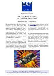
Technical Information CCK-MARIMBA Mezzanine I/O Expansion - Ekf
Technical Information CCK-MARIMBA Mezzanine I/O Expansion - Ekf
Technical Information CCK-MARIMBA Mezzanine I/O Expansion - Ekf

Create successful ePaper yourself
Turn your PDF publications into a flip-book with our unique Google optimized e-Paper software.
<strong>Technical</strong> <strong>Information</strong><br />
<strong>CCK</strong>-<strong>MARIMBA</strong><br />
<strong>Mezzanine</strong> I/O <strong>Expansion</strong> Board<br />
PMC/XMC Module Carrier<br />
Document No. 5098 • Ed. 6 • 26 September 2012
<strong>Technical</strong> <strong>Information</strong> <strong>CCK</strong>-<strong>MARIMBA</strong> • PMC/XMC Module Carrier<br />
Contents<br />
About this Manual ........................................................... 4<br />
Edition History......................................................... 4<br />
Related Documents ..................................................... 5<br />
Nomenclature ......................................................... 5<br />
Trade Marks .......................................................... 5<br />
Legal Disclaimer - Liability Exclusion ......................................... 5<br />
Standards ............................................................ 6<br />
<strong>CCK</strong>-<strong>MARIMBA</strong> Features....................................................... 7<br />
Short Description....................................................... 9<br />
Front Panel .......................................................... 15<br />
Block Diagram........................................................ 16<br />
Top View............................................................ 21<br />
On-Board Connectors .................................................. 22<br />
Jumpers ............................................................ 23<br />
Inter-Board Connectors ................................................. 23<br />
Rear I/O Connectors ................................................... 23<br />
Installing and Replacing Components............................................ 24<br />
Before You Begin...................................................... 24<br />
Warnings ...................................................... 24<br />
Caution ....................................................... 24<br />
Installing the Board .................................................... 25<br />
Removing the Board ................................................... 26<br />
EMC Recommendations................................................. 27<br />
<strong>Technical</strong> Reference - Connectors ............................................... 28<br />
Caution............................................................. 28<br />
Please Note .......................................................... 28<br />
On-Board Connectors .................................................. 29<br />
PMC Socket Receptacles J11 J12 J14 .................................. 29<br />
XMC Socket Receptacles J15 J16..................................... 33<br />
P-IDE2 ........................................................ 36<br />
P-SATA1 ....................................................... 37<br />
P-SATA2 P-SATA3................................................ 41<br />
P-SP3 P-SP4 .................................................... 42<br />
P-UFD2........................................................ 44<br />
On-Board Jumpers..................................................... 45<br />
J-RES Reset ..................................................... 45<br />
J-FWH2 ....................................................... 45<br />
Inter-Board Connectors ................................................. 46<br />
P-EXP ......................................................... 48<br />
P-PCIE......................................................... 49<br />
Rear I/O Connectors ................................................... 50<br />
J1 J2.......................................................... 50<br />
Additional Functions ........................................................ 53<br />
Firmware Hub 2 ...................................................... 53<br />
SMBus EEPROM ...................................................... 53<br />
Trusted Platform Module................................................ 54<br />
© EKF -2- ekf.com
<strong>Technical</strong> <strong>Information</strong> <strong>CCK</strong>-<strong>MARIMBA</strong> • PMC/XMC Module Carrier<br />
Power Distribution .......................................................... 55<br />
Schematics................................................................ 56<br />
© EKF -3- ekf.com
About this Manual<br />
<strong>Technical</strong> <strong>Information</strong> <strong>CCK</strong>-<strong>MARIMBA</strong> • PMC/XMC Module Carrier<br />
This manual is a short form description of the technical aspects of the <strong>CCK</strong>-<strong>MARIMBA</strong>, required for<br />
installation and system integration. It is intended for the advanced user only.<br />
Edition History<br />
EKF<br />
Document<br />
Text # 5098<br />
cck_tie.wpd<br />
Ed. Contents/Changes Author Date<br />
1 <strong>Technical</strong> <strong>Information</strong> <strong>CCK</strong>-<strong>MARIMBA</strong><br />
English, preliminary edition<br />
jj 13 March 2008<br />
2 Added photos jj 6 January 2009<br />
3 Added photos top/bottom view jj 22 October<br />
2009<br />
4 Added photos <strong>CCK</strong>-<strong>MARIMBA</strong> exploded<br />
view, added photos C20-SATA<br />
5 Added photos <strong>CCK</strong>-<strong>MARIMBA</strong> with<br />
CCM-BOOGIE CPU carrier card<br />
6 Added photo <strong>CCK</strong>-<strong>MARIMBA</strong> with<br />
DU1-MUSTANG XMC Module<br />
jj 17 November<br />
2009<br />
jj 17 August 2011<br />
jj 26 September<br />
2012<br />
© EKF -4- ekf.com
Related Documents<br />
<strong>Technical</strong> <strong>Information</strong> <strong>CCK</strong>-<strong>MARIMBA</strong> • PMC/XMC Module Carrier<br />
For a description of the CCG-RUMBA or CCM-BOOGIE CPU cards, which act as base boards with<br />
respect to the <strong>CCK</strong>-<strong>MARIMBA</strong>, please refer to the correspondent CPU user guide, available by<br />
download from either www.ekf.com/c/ccpu/ccg/ccg_e.html or www.ekf.com/c/ccpu/ccm/ccm_e.html.<br />
Nomenclature<br />
Signal names used herein with an attached '#' designate active low lines.<br />
Trade Marks<br />
Some terms used herein are property of their respective owners, e.g.<br />
< Intel, Pentium, Celeron, Pentium M, Core 2 Duo, Merom, Penryn, iAMT: ® Intel<br />
< Santa Rosa Platform, Crestline Chipset GM965, Matanzas CRB: Intel<br />
< CompactPCI ® : ® PICMG<br />
< Windows 2000, Windows XP, Windows Vista: ® Microsoft<br />
< EKF, ekf system: ® EKF<br />
EKF does not claim this list to be complete.<br />
Legal Disclaimer - Liability Exclusion<br />
This manual has been edited as carefully as possible. We apologize for any potential mistake.<br />
<strong>Information</strong> provided herein is designated exclusively to the proficient user (system integrator,<br />
engineer). EKF can accept no responsibility for any damage caused by the use of this manual.<br />
© EKF -5- ekf.com
Standards<br />
<strong>Technical</strong> <strong>Information</strong> <strong>CCK</strong>-<strong>MARIMBA</strong> • PMC/XMC Module Carrier<br />
PMC IEEE P1386.1<br />
XMC VITA 42.3<br />
Specifications/Standards<br />
CompactPCI PICMG 2.0 (www.picmg.org)<br />
PCI Local Bus PCI 2.2/2.3/3.0 Standards (PCI SIG www.pcisig.com)<br />
PCI Express PCIe Base Spec. 1.1 and other (PCI SIG www.pcisig.com)<br />
SATA Serial ATA 2.5/2.6 Specification (www.sata-io.org)<br />
USB Universal Serial Bus Revision 2.0 specification (www.usb.org/developers)<br />
TPM Trusted Platform Module 1.2<br />
(https://www.trustedcomputinggroup.org)<br />
© EKF -6- ekf.com
<strong>CCK</strong>-<strong>MARIMBA</strong> Features<br />
<strong>Technical</strong> <strong>Information</strong> <strong>CCK</strong>-<strong>MARIMBA</strong> • PMC/XMC Module Carrier<br />
Feature Summary<br />
Form Factor Single size Eurocard (160x100mm 2 ), needs 4HP (20.3mm) mounting space in addition to<br />
CPU carrier board, typically delivered as a ready to use assembly unit (including the CCG-<br />
RUMBA or successor CPU card), provided with a common 8HP front panel shared with the<br />
CPU board, mounting position right (on top of CPU board)<br />
XMC Module<br />
Carrier Function 5<br />
PMC Module<br />
Carrier Function 5<br />
PCIe Packet Switch<br />
PCIe Usage<br />
SATA/PATA 3<br />
LPC Super-I/O 3<br />
(SIO2)<br />
Firmware Hub 3<br />
(FWH2)<br />
TPM 3<br />
Front Panel<br />
Connectors<br />
Host I/F Connectors<br />
(to CPU Carrier) 1<br />
On-Board I/O<br />
Connectors 1<br />
Rear I/O Connector<br />
Option 1<br />
Carrier for single width XMC mezzanine card (149mm x 74mm) according to VITA<br />
42.0/42.3, connectors J15, J16, suitable for PCIe x 4 (x 1, x 2) XMC modules, J16 may be<br />
used for custom specific rear I/O via J1<br />
Carrier for single width PMC mezzanine card (149mm x 74mm) according to IEEE 1386.1,<br />
connectors J11, J12, J14, PCI interface 32-bit 33MHz, J14 may be used for custom specific<br />
rear I/O via J1<br />
< PCIe packet switch 3 ports, 4 lanes each (12 lanes in total)<br />
< 4 Lanes (configured as 1 link x 4 lanes) to host (carrier board ICH)<br />
< 4 Lanes assigned to XMC module socket J15<br />
< 1 Lane dedicated to PCIe/PCI bridge (PMC PCI I/F)<br />
< 1 Lane dedicated to SATA/PATA controller<br />
SMB363 PCIe to 2 x SATA II / 1 x PATA controller, RAID level 0/1 capable<br />
SCH3114, parallel port, 4 serial ports, PS/2 keyboard & mouse port, GPIO (available via rear<br />
I/O J2 connector)<br />
82802 generic device, 8Mbit Flash, LPC interface, can be switched as secondary or primary<br />
(boot code) FWH<br />
Option Trusted Platform Module cryptographic chip according to TPM 1.2<br />
Bezel for PMC/XMC cutout, to be removed when mezzanine module with front panel I/O is<br />
inserted<br />
< PCI Express interface (PCIe x 4)<br />
< Multifunction expansion interface (LPC, USB, SMB)<br />
< PMC: J11, J12 - PCI I/F J14 - Rear I/O (to J1)<br />
< XMC: J15 - PCIe I/F J16 - Rear I/O (to J1)<br />
< Connector for mounting of optional C20-SATA mezzanine card with 1 or 2 SATA<br />
drives 2.5-inch (RAID capable)<br />
< 2 x Latched SATA headers 7-pos. (option)<br />
< Socket for C17-CFA CompactFlash mezzanine module (bottom mount)<br />
< Header suitable for USB Solid State Drive (SSD) module (bottom mount)<br />
< 2 x Serial port headers (TTL-level)<br />
< Reset<br />
Optional J1/J2 2.0mm hard metric connectors (CompactPCI style with proprietary signal<br />
mapping) for custom specific transition module or backplane, major signal groups:<br />
< Parallel Port (LPT)<br />
< COM ports 1 - 4 (TTL-level UART signals)<br />
< PS/2 keyboard & mouse<br />
< GPIO<br />
< SMBus<br />
< PMC custom specific rear I/O (from J14)<br />
< XMC custom specific rear I/O (from J16)<br />
On-Board Functions Speaker, LEDs, SMBus EEPROM, temperature sensors<br />
Mass Storage<br />
Options 2<br />
< C20-SATA mezzanine card with 1 or 2 SATA drives 2.5-inch<br />
< Up to 2 external SATA drives attached to SATA headers<br />
< C17-CFA (bottom mount) CompactFlash module<br />
< USB Solid State Drive (SSD) module option (bottom mount)<br />
© EKF -7- ekf.com
1<br />
2<br />
3<br />
4<br />
5<br />
Thermal<br />
Conditions 4<br />
Environmental<br />
Conditions 4<br />
<strong>Technical</strong> <strong>Information</strong> <strong>CCK</strong>-<strong>MARIMBA</strong> • PMC/XMC Module Carrier<br />
< Operating temperature: 0°C ... +70°C<br />
< Storage temperature: -40°C ... +85°C, max. gradient 5°C/min<br />
< Humidity 5% ... 95% RH non condensing<br />
< Altitude -300m ... +3000m<br />
< Shock 15g 0.33ms, 6g 6ms<br />
< Vibration 1g 5-2000Hz<br />
EC Regulations < EN55022, EN55024, EN60950-1 (UL60950-1/IEC60950-1)<br />
< 2002/95/EC (RoHS)<br />
MTBF tbd<br />
Not all of these connectors may be present or functional on your actual <strong>CCK</strong>-<strong>MARIMBA</strong> board.<br />
Assembly of these connectors is highly custom specific. Discuss your needs with EKF before<br />
ordering.<br />
Options may be exclusive, i.e. not necessarily concurrently present. Ask EKF for special solutions<br />
if required.<br />
Silicon/function may not be present on your actual <strong>CCK</strong>-<strong>MARIMBA</strong> board. Assembly of<br />
components is highly custom specific. Discuss your needs with EKF before ordering.<br />
Hard disk option may require decrease<br />
Either one - XMC or PMC module - can be accommodated, exclusively to each other<br />
© EKF -8- ekf.com
Short Description<br />
<strong>Technical</strong> <strong>Information</strong> <strong>CCK</strong>-<strong>MARIMBA</strong> • PMC/XMC Module Carrier<br />
Available as a mezzanine add-on expansion<br />
board to the CCG-RUMBA and successor CPU<br />
cards, the <strong>CCK</strong>-<strong>MARIMBA</strong> provides a number of<br />
additional I/O functions. First of all, the <strong>CCK</strong>-<br />
<strong>MARIMBA</strong> itself is a carrier board, suitable for<br />
accommodation of either a single width PMC or<br />
XMC module.<br />
The additional SATA/PATA controller is useful<br />
for attachment of mass-storage devices, either<br />
on-board mounted, or externally (by cable).<br />
Furthermore the <strong>CCK</strong>-<strong>MARIMBA</strong> is equipped<br />
with a SIO, which provides legacy I/O ports,<br />
such as serial, parallel, KB/MS (all available<br />
across rear I/O).<br />
A secondary Firmware Hub can be configured<br />
as alternate- or backup-BIOS.<br />
Another option available is the Trusted Platform<br />
Module according to TPM 1.2 for safety critical<br />
applications.<br />
The <strong>CCK</strong>-<strong>MARIMBA</strong> will be attached on top of<br />
the CPU carrier board, and typically shares its<br />
front panel with the host carrier (usually 8HP<br />
front panel width in total). Interconnection<br />
between the <strong>CCK</strong>-<strong>MARIMBA</strong> I/O module and<br />
the CPU carrier board is achieved by two<br />
expansion connectors, which comprise the PCIe<br />
(PCI Express x 4) and LPC (Low Pin Count)<br />
interfaces.<br />
As an option, the <strong>CCK</strong>-<strong>MARIMBA</strong> is available<br />
with a mezzanine module (C20-SATA), which<br />
accommodates one or two 2.5-inch SATA hard<br />
disk drives (RAID option). Additionally, a<br />
CompactFlash card adapter can be mounted on<br />
bottom of the <strong>CCK</strong>-<strong>MARIMBA</strong>.<br />
© EKF -9- ekf.com
<strong>Technical</strong> <strong>Information</strong> <strong>CCK</strong>-<strong>MARIMBA</strong> • PMC/XMC Module Carrier<br />
The <strong>CCK</strong>-<strong>MARIMBA</strong> communicates by means of<br />
2 bottom mount expansion connectors with the<br />
host CPU: P-PCIE (PCI Express x 4), and P-EXP<br />
(multi-function I/F such as LPC, USB, SMB).<br />
The PCI Express interface (connector P-PCIE) is<br />
comprised of 4 PCIe lanes, which are derived<br />
from the ICH (southbridge chip) on the CPU<br />
carrier board. All 4 lanes are routed to the<br />
primary port of a 3-port 12-lane PCI Express<br />
packet switch, which is the main component of<br />
the <strong>CCK</strong>-<strong>MARIMBA</strong>.<br />
Connector P-EXP combines several other<br />
southbridge data channels: The LPC (Low Pin<br />
Count) is a multiplexed ISA bus, e.g. enabling<br />
the super-I/O (SIO) controller chip to emulate<br />
the legacy I/O interfaces; among these are the<br />
classic parallel (printer) and serial (COM) ports.<br />
Two USB channels are provided, one for the<br />
optional USB SSD, and one or both for rear I/O<br />
via the J2 connector.<br />
The Trusted Platform Module is an optionally<br />
available cryptographic chip, which provides a<br />
comprehensive hardware and software solution<br />
for safer computing. Conforming to the TPM1.2<br />
standard of the TCG, the TPM is comprised of a<br />
16-bit security controller and additional<br />
hardware e.g. to generate 2048 bit RSA keys<br />
and true random numbers, thus meeting the<br />
highest industry rating for digital security.<br />
The <strong>CCK</strong>-<strong>MARIMBA</strong> fits on the top side of the<br />
CPU board, which is on the right side when<br />
viewing the common front panel. A suitable<br />
backplane provides its CPCI slots beginning with<br />
the CPU carrier board (CPCI system slot) from<br />
right to left. The CPCI system must provide<br />
additional mounting space to the right side for<br />
the <strong>CCK</strong>-<strong>MARIMBA</strong>. In addition, a single slot<br />
rear I/O backplane would be needed for rear I/O<br />
usage, and a custom specific rear I/O transition<br />
module.<br />
© EKF -10- ekf.com
<strong>Technical</strong> <strong>Information</strong> <strong>CCK</strong>-<strong>MARIMBA</strong> • PMC/XMC Module Carrier<br />
CPU Board • PMC/XMC Carrier Side Card • DE1-FOX PMC Module<br />
© EKF -11- ekf.com
<strong>Technical</strong> <strong>Information</strong> <strong>CCK</strong>-<strong>MARIMBA</strong> • PMC/XMC Module Carrier<br />
CPU Board • PMC/XMC Carrier Side Card • DX1-LYNX XMC Module (Dual Drive)<br />
© EKF -12- ekf.com
<strong>Technical</strong> <strong>Information</strong> <strong>CCK</strong>-<strong>MARIMBA</strong> • PMC/XMC Module Carrier<br />
CPU Board • PMC/XMC Carrier Side Card • DU1-MUSTANG XMC Module<br />
© EKF -13- ekf.com
<strong>Technical</strong> <strong>Information</strong> <strong>CCK</strong>-<strong>MARIMBA</strong> • PMC/XMC Module Carrier<br />
P1<br />
Single-Slot Rear I/O Backplane (Option)<br />
CPCI System Slot<br />
CompactPCI Backplane<br />
P2 P2 P2<br />
As of current, the suitable CPU carrier board for use together with the <strong>CCK</strong>-<strong>MARIMBA</strong> mezzanine<br />
module is the CCG-RUMBA (successor CCM-BOOGIE available late 2008). The <strong>CCK</strong>-<strong>MARIMBA</strong><br />
expansion board mounts on top (at the right side) of the CCG-RUMBA.<br />
If the CompactPCI backplane is provided with a right aligned system slot, be sure to position the CPU<br />
carrier board to the rightmost CPCI slot (and not the <strong>CCK</strong>-<strong>MARIMBA</strong>). Consequently, the <strong>CCK</strong>-<br />
<strong>MARIMBA</strong> then occupies the next card slot to the right, outside of the CPCI backplane, which may be<br />
provided with a single slot rear I/O P1/P2 backplane. In order to make use of the rear I/O capability of<br />
the <strong>CCK</strong>-<strong>MARIMBA</strong>, its optional J1/J2 rear I/O connectors must be stuffed (consider before ordering).<br />
This assembly order (right aligned CPCI system slot) is preferred because no CompactPCI slot is lost in<br />
a system for the <strong>CCK</strong>-<strong>MARIMBA</strong>.<br />
Vice versa, if a CPCI backplane is mandatory with a left aligned system slot, the <strong>CCK</strong>-<strong>MARIMBA</strong> must<br />
not be equipped with J1/J2 connectors, and occupies a regular CompactPCI slot then. Of course, this<br />
assembly solution is not suitable for rear I/O with the <strong>CCK</strong>-<strong>MARIMBA</strong>, and a CPCI slot will be lost. With<br />
J1/J2 stuffed, a coding key present on J1 would prevent insertion of the <strong>CCK</strong>-<strong>MARIMBA</strong> into a CPCI<br />
card slot.<br />
P1 P2 P1<br />
© EKF<br />
ekf.com<br />
<strong>CCK</strong>-<strong>MARIMBA</strong> on Top of the CPU Carrier<br />
© EKF -14- ekf.com<br />
J2<br />
J1
Front Panel<br />
<strong>Technical</strong> <strong>Information</strong> <strong>CCK</strong>-<strong>MARIMBA</strong> • PMC/XMC Module Carrier<br />
CCG-<br />
RUMBA<br />
D<br />
V<br />
I<br />
-<br />
I<br />
P<br />
G<br />
G<br />
P<br />
H<br />
D<br />
USB<br />
G-ETH<br />
CCG-RUMBA<br />
DVI<br />
<strong>CCK</strong>-<br />
<strong>MARIMBA</strong><br />
<strong>CCK</strong>-<br />
<strong>MARIMBA</strong><br />
Typically the CCG-RUMBA carrier board CPU and the <strong>CCK</strong>-<strong>MARIMBA</strong> share a common 3U/8HP front<br />
panel. Not shown in the illustration above are variations of the CCG-RUMBA (e.g. with VGA connector<br />
rather than DVI).<br />
There may be reasons for further widening of the front panel (e.g. 12HP width); this would provide<br />
additional space e.g. for serial port connectors (CU-series modules). Please discuss your needs for an<br />
individual solution with EKF.<br />
© EKF -15- ekf.com<br />
X<br />
M<br />
C<br />
P<br />
M<br />
C<br />
M<br />
E<br />
Z<br />
Z<br />
A<br />
N<br />
I<br />
N<br />
E<br />
draft only - do not scale • © EKF • ekf.com
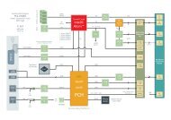
Block Diagram<br />
<strong>Technical</strong> <strong>Information</strong> <strong>CCK</strong>-<strong>MARIMBA</strong> • PMC/XMC Module Carrier<br />
Simplified Block Diagram<br />
<strong>CCK</strong>-<strong>MARIMBA</strong><br />
Sheet 2<br />
XMC J15<br />
Carrier-<br />
Board<br />
PCI Express<br />
PCIe<br />
Packet<br />
Switch<br />
PCI Express<br />
Sheet 2<br />
PCI Bridge<br />
Sheet 3<br />
SATA Bridge<br />
Sheet 1/5<br />
PCI Express<br />
3-Port/12-Lane<br />
Packet Switch<br />
© EKF -16- ekf.com
<strong>Technical</strong> <strong>Information</strong> <strong>CCK</strong>-<strong>MARIMBA</strong> • PMC/XMC Module Carrier<br />
Simplified Block Diagram<br />
<strong>CCK</strong>-<strong>MARIMBA</strong><br />
PCIe Switch<br />
Sheet 1<br />
PCI Express<br />
PCI PMC<br />
PCIe<br />
PCIe Switch<br />
Sheet 1<br />
to<br />
PCI<br />
PCI 32-bit<br />
33/66MHz<br />
11 12<br />
15<br />
PCIe x 4<br />
XMC<br />
Option<br />
PMC<br />
RIO<br />
XMC<br />
XMC/PMC<br />
<strong>Mezzanine</strong><br />
PMC Rear I/O<br />
J14/P14 (64 I/O signals)<br />
14<br />
13<br />
16<br />
Ext. Pwr.<br />
Option<br />
Rear I/O<br />
RIO PMC<br />
+5V/+3.3V/+12V/-12V<br />
J1<br />
XMC Rear I/O<br />
J16/P16 rows C & F - 38 user definable signals<br />
Sheet 2/5<br />
PMC/XMC Socket<br />
Front<br />
Panel<br />
I/O<br />
© EKF -17- ekf.com
<strong>Technical</strong> <strong>Information</strong> <strong>CCK</strong>-<strong>MARIMBA</strong> • PMC/XMC Module Carrier<br />
PCIe Switch<br />
Sheet 1<br />
PCIe<br />
SATA<br />
PATA<br />
SATA II<br />
3Gbps<br />
2.5-Inch SATA<br />
Hard Hard Disk Disk Drives Drive<br />
Controller<br />
SATA lanes<br />
available<br />
either for<br />
P-SATA1/2<br />
or C20-SATA<br />
Top & Bottom Mount<br />
C20-SATA<br />
Optional<br />
Single/Dual Drive<br />
C20-SATA<br />
<strong>Mezzanine</strong> Module<br />
Simplified Block Diagram<br />
<strong>CCK</strong>-<strong>MARIMBA</strong><br />
PATA<br />
Sheet 3/5<br />
Option<br />
SATA Storage<br />
P-IDE1/2<br />
CompactFlash<br />
C10-CFA C17-CFA<br />
Optional<br />
C10-CFA (top mount)<br />
C17-CFA (bottom mount)<br />
CompactFlash / SSD Module<br />
© EKF -18- ekf.com
SMB<br />
43<br />
00<br />
SMB (+5V)<br />
Sheet 5<br />
J2<br />
<strong>Technical</strong> <strong>Information</strong> <strong>CCK</strong>-<strong>MARIMBA</strong> • PMC/XMC Module Carrier<br />
SWITCH<br />
EEPROM<br />
I2C<br />
Speaker<br />
SPK<br />
Simplified Block Diagram<br />
<strong>CCK</strong>-<strong>MARIMBA</strong><br />
Sheet 5<br />
J2<br />
USB<br />
Sheet 4/5<br />
Option<br />
SIO - FWH - TPM<br />
Sheet 5<br />
J2<br />
Carrier-<br />
Board<br />
Option<br />
Trusted<br />
Platform<br />
Module<br />
SER1<br />
TTL<br />
Sheet 5<br />
J2<br />
TPM<br />
1.2<br />
GP40<br />
Crypto<br />
Engine<br />
SER2<br />
Sheet 5<br />
TTL<br />
SER3<br />
Sheet 5<br />
LPC<br />
LPC<br />
TTL<br />
SER4<br />
Sheet 5<br />
TTL<br />
J2<br />
Sheet 5<br />
GPI<br />
82<br />
802<br />
© EKF -19- ekf.com<br />
J2<br />
J2<br />
J2<br />
FWH2<br />
Par.<br />
Printer<br />
Sheet 5<br />
J2<br />
GP44<br />
J-FWH<br />
Keybd<br />
Mouse<br />
Sheet 5<br />
J2<br />
Sheet 5<br />
J2
<strong>Technical</strong> <strong>Information</strong> <strong>CCK</strong>-<strong>MARIMBA</strong> • PMC/XMC Module Carrier<br />
SMB (+5V)<br />
Sheet 4<br />
I2C Switch<br />
Level Shift<br />
GPIO (SIO - FWH)<br />
Rear I/O<br />
Sheet 4<br />
SIO - FWH<br />
Simplified Block Diagram<br />
<strong>CCK</strong>-<strong>MARIMBA</strong><br />
SP1..4 (TTL UART), LPT<br />
Sheet 4<br />
SIO<br />
PS/2 KB/MS<br />
Sheet 4<br />
SIO<br />
J2<br />
USB<br />
Sheet 4<br />
P-EXP<br />
Sheet 5/5<br />
J2 Rear I/O<br />
Option<br />
SanDisk SDUS5EB<br />
STec SLUFDM<br />
Intel Z-U130 SSDUSMS<br />
4GB/8GB<br />
USB<br />
P-UFD<br />
USB<br />
Alternates<br />
P-UFD2 - Bottom Mount<br />
Flash Drive<br />
(SSD) Option<br />
© EKF -20- ekf.com
Top View<br />
<strong>Technical</strong> <strong>Information</strong> <strong>CCK</strong>-<strong>MARIMBA</strong> • PMC/XMC Module Carrier<br />
Assembly w/o PMC/XMC Module<br />
Assembly with PMC/XMC Module<br />
© EKF -21- ekf.com
On-Board Connectors<br />
1<br />
2<br />
<strong>Technical</strong> <strong>Information</strong> <strong>CCK</strong>-<strong>MARIMBA</strong> • PMC/XMC Module Carrier<br />
J11, J12 PMC module, PCI interface<br />
J14 PMC module, rear I/O option<br />
J15 XMC module, PCI Express interface<br />
J16 XMC module, rear I/O option<br />
P-IDE2 PATA socket (bottom mount), suitable for C17-CFA CompactFlash module<br />
P-SATA1 Microspeed female connector, for top mount attachment of a C20-SATA mezzanine<br />
module, equipped with either one or two SATA drives 2.5-inch (RAID option with 2 drives)<br />
P-SATA2<br />
P-SATA3<br />
P-SP3 1<br />
P-SP4<br />
P-UFD2 2<br />
Vertical latched SATA header, 7-position, stuffing option (exclusive to P-SATA1)<br />
Pin headers 10-lead 2.00mm, provide TTL level serial COM port signals (CU-series<br />
modules)<br />
Socket (bottom mount) 10-lead 2.00mm pitch, for low profile USB SSD (Solid State Drive)<br />
Due to a primary SIO which may be present on the CPU board itself, the BIOS may assign COM port numbers<br />
different from COM3/COM4 to these interface lines on the <strong>CCK</strong>-<strong>MARIMBA</strong>, e.g. COM4/COM5.<br />
USB channel shared (stuffing option) with J2 for rear I/O<br />
© EKF -22- ekf.com
Jumpers<br />
1<br />
J-FWH 1<br />
J-RES 1<br />
<strong>Technical</strong> <strong>Information</strong> <strong>CCK</strong>-<strong>MARIMBA</strong> • PMC/XMC Module Carrier<br />
Jumper 2.54mm, determines if the optional on-board firmware hub is acting as<br />
boot BIOS (jumper set) or as secondary BIOS (jumper removed = default).<br />
Jumper 2.54mm, allows to force a CPU debug reset on the CCG-RUMBA CPU carrier<br />
board<br />
Not all of these jumpers may be present or functional on your actual <strong>CCK</strong>-<strong>MARIMBA</strong> board. Assembly of these<br />
jumpers is highly custom specific. Discuss your needs with EKF before ordering.<br />
Inter-Board Connectors<br />
P-EXP Dual row socket, available from bottom of the <strong>CCK</strong>-<strong>MARIMBA</strong> PCB, matching with the<br />
corresponding socket on the CPU carrier board, connected through a board stacker,<br />
comprising of:<br />
• LPC Low Pin Count interface<br />
• AC'97 Audio Codec / HD Audio (Azalia)<br />
• 2 x USB<br />
• SMB, Speaker, Reset<br />
P-PCIE High speed socket edge card connector, available from bottom of the <strong>CCK</strong>-<strong>MARIMBA</strong> PCB,<br />
matching with the corresponding socket on the CPU carrier board, connected through a<br />
high speed strip line PCB (C22), comprising of:<br />
• Host CPU (ICH8) PCI Express (PCIe) x 4 interface<br />
Rear I/O Connectors<br />
2<br />
J1 2<br />
J2 2<br />
Please note:<br />
J1/J2 are optional<br />
2.00mm brown keyed Hard Metric female connector, signal groups PMC rear I/O, XMC<br />
rear I/O<br />
2.00mm Hard Metric female connector, signal groups GPIO, parallel port, serial ports (TTLlevel<br />
signals), USB, SMB (+5V), speaker<br />
Not all of the connectors or other elements listed above may be present or functional on your actual<br />
<strong>CCK</strong>-<strong>MARIMBA</strong> board. Assembly of these connectors is highly custom specific. Discuss your needs<br />
(target application) with EKF before ordering, for an optimum board configuration.<br />
© EKF -23- ekf.com
<strong>Technical</strong> <strong>Information</strong> <strong>CCK</strong>-<strong>MARIMBA</strong> • PMC/XMC Module Carrier<br />
Installing and Replacing Components<br />
Before You Begin<br />
Warnings<br />
The procedures in this chapter assume familiarity with the general terminology associated with<br />
industrial electronics and with safety practices and regulatory compliance required for using and<br />
modifying electronic equipment. Disconnect the system from its power source and from<br />
any telecommunication links, networks or modems before performing any of the<br />
procedures described in this chapter. Failure to disconnect power, or telecommunication<br />
links before you open the system or perform any procedures can result in personal injury<br />
or equipment damage. Some parts of the system can continue to operate even though<br />
the power switch is in its off state.<br />
Caution<br />
Electrostatic discharge (ESD) can damage components. Perform the procedures described in this<br />
chapter only at an ESD workstation. If such a station is not available, you can provide<br />
some ESD protection by wearing an antistatic wrist strap and attaching it to a<br />
metal part of the system chassis or board front panel. Store the board only in its<br />
original ESD protected packaging. Retain the original packaging (antistatic bag and<br />
antistatic box) in case of returning the board to EKF for repair.<br />
© EKF -24- ekf.com
Installing the Board<br />
Warning<br />
<strong>Technical</strong> <strong>Information</strong> <strong>CCK</strong>-<strong>MARIMBA</strong> • PMC/XMC Module Carrier<br />
This procedure should be done only by qualified technical personnel. Disconnect the system from its<br />
power source before doing the procedures described here. Failure to disconnect power, or<br />
telecommunication links before you open the system or perform any procedures can result in personal<br />
injury or equipment damage.<br />
Typically you will perform the following steps:<br />
C Switch off the system, remove the AC power cord<br />
C Attach your antistatic wrist strap to a metallic part of the system<br />
C Remove the board packaging, be sure to touch the board only at the front panel<br />
C Identify the related CompactPCI slot (peripheral slot for I/O boards, system slot for CPU boards,<br />
with the system slot typically most right or most left to the backplane)<br />
C Insert card carefully (be sure not to damage components mounted on the bottom side of the<br />
board by scratching neighboured front panels)<br />
C A card with onboard connectors requires attachment of associated cabling now<br />
C Lock the ejector lever, fix screws at the front panel (top/bottom)<br />
C Retain original packaging in case of return<br />
© EKF -25- ekf.com
Removing the Board<br />
Warning<br />
<strong>Technical</strong> <strong>Information</strong> <strong>CCK</strong>-<strong>MARIMBA</strong> • PMC/XMC Module Carrier<br />
This procedure should be done only by qualified technical personnel. Disconnect the system from its<br />
power source before doing the procedures described here. Failure to disconnect power, or<br />
telecommunication links before you open the system or perform any procedures can result in personal<br />
injury or equipment damage.<br />
Typically you will perform the following steps:<br />
C Switch off the system, remove the AC power cord<br />
C Attach your antistatic wrist strap to a metallic part of the system<br />
C Identify the board, be sure to touch the board only at the front panel<br />
C unfasten both front panel screws (top/bottom), unlock the ejector lever<br />
C Remove any onboard cabling assembly<br />
C Activate the ejector lever<br />
C Remove the card carefully (be sure not to damage components mounted on the bottom side<br />
of the board by scratching neighboured front panels)<br />
C Store board in the original packaging, do not touch any components, hold the board at the<br />
front panel only<br />
Warning<br />
Do not expose the card to fire. Battery cells and other components could explode<br />
and cause personal injury.<br />
© EKF -26- ekf.com
EMC Recommendations<br />
<strong>Technical</strong> <strong>Information</strong> <strong>CCK</strong>-<strong>MARIMBA</strong> • PMC/XMC Module Carrier<br />
In order to comply with the CE regulations for EMC, it is mandatory to observe the following rules:<br />
C The chassis or rack including other boards in use must comply entirely with CE<br />
C Close all board slots not in use with a blind front panel<br />
C Front panels must be fastened by built-in screws<br />
C Cover any unused front panel mounted connector with a shielding cap<br />
C External communications cable assemblies must be shielded (shield connected only at one end<br />
of the cable)<br />
C Use ferrite beads for cabling wherever appropriate<br />
C Some connectors may require additional isolating parts<br />
Reccomended Accessories<br />
Blind CPCI Front<br />
Panels<br />
Ferrit Bead Filters ARP Datacom,<br />
63115 Dietzenbach<br />
Metal Shielding<br />
Caps<br />
EKF Elektronik Widths currently available<br />
(1HP=5.08mm):<br />
with handle 4HP/8HP<br />
without handle<br />
2HP/4HP/8HP/10HP/12HP<br />
Conec-Polytronic,<br />
59557 Lippstadt<br />
Ordering No.<br />
102 820 (cable diameter 6.5mm)<br />
102 821 (cable diameter 10.0mm)<br />
102 822 (cable diameter 13.0mm)<br />
Ordering No.<br />
CDFA 09 165 X 13129 X (DB9)<br />
CDSFA 15 165 X 12979 X (DB15)<br />
CDSFA 25 165 X 12989 X (DB25)<br />
© EKF -27- ekf.com
<strong>Technical</strong> <strong>Information</strong> <strong>CCK</strong>-<strong>MARIMBA</strong> • PMC/XMC Module Carrier<br />
<strong>Technical</strong> Reference - Connectors<br />
Caution<br />
Some of the connectors may provide operating voltage (e.g. +12V, +5V and +3.3V) to devices inside<br />
the system chassis, such as internal peripherals. Not all of these connectors are overcurrent protected.<br />
Do not use these connectors for powering devices external to the computer chassis. A fault in the load<br />
presented by the external devices could cause damage to the board, the interconnecting cable and<br />
the external devices themselves.<br />
Please Note<br />
The <strong>CCK</strong>-<strong>MARIMBA</strong> mezzanine module may be equipped with several on-board connectors for system<br />
internal usage. Not all of these connectors may be present on a particular board. Be sure to specify<br />
your individual needs when ordering the <strong>CCK</strong>-<strong>MARIMBA</strong> board. Characteristic features and the pin<br />
assignments of each connector are described on the following pages (connector designation in<br />
alphabetical order within the groups 'on-board connectors', 'inter-board connectors', and 'rear I/O<br />
connectors').<br />
© EKF -28- ekf.com
On-Board Connectors<br />
<strong>Technical</strong> <strong>Information</strong> <strong>CCK</strong>-<strong>MARIMBA</strong> • PMC/XMC Module Carrier<br />
The <strong>CCK</strong>-<strong>MARIMBA</strong> can be equipped with several on-board connectors. Some of these connectors are<br />
available as an option only or exclusive to each other, and therefore may not be functional or even<br />
present on your actual board.<br />
Assembly of these connectors is highly custom specific. Discuss your needs with EKF before ordering,<br />
so that the optimum board configuration for your application will be chosen.<br />
PMC Socket Receptacles J11 J12 J14<br />
The <strong>CCK</strong>-<strong>MARIMBA</strong> is a PMC carrier board with 32-bit PCI host interface. Hence, 3 (of max. 4) IEEE<br />
P.1386 PMC connectors are provided, PMC-J11, -J12 and -J14. There is no need for -J13 which would<br />
be a requirement for 64-bit PCI only. The 32-bit PCI interface is comprised of PMC-J11 and -J12, while<br />
PMC-J14 is reserved for optional rear I/O usage across the connector J1 (custom specific rear I/O<br />
transition module). A custom specific rear I/O transition module can be discussed with EKF<br />
(sales@ekf.de).<br />
The PMC module PCI host interface is provided by the PCI Express to PCI bridge PEX8112, which is<br />
connected to the PCI Express packet switch. The PCI interface VIO voltage is set to +3.3V by default.<br />
If required, +5V is also available as PCI VIO, by means of a stuffing option.<br />
© EKF -29- ekf.com
1)<br />
2)<br />
3)<br />
4)<br />
<strong>Technical</strong> <strong>Information</strong> <strong>CCK</strong>-<strong>MARIMBA</strong> • PMC/XMC Module Carrier<br />
1 2<br />
Part No. 275.01.08.064.03 • © EKF • ekf.com<br />
IEEE1386 Receptacle<br />
63 64<br />
PMC-J11 - PCI<br />
1 TCK -12V 4)<br />
2<br />
3 GND INTA# 4<br />
5 INTB# INTC# 6<br />
7 BUSMODE1# 1)<br />
+5V 8<br />
9 INTD# Reserved 10<br />
11 GND +3.3V<br />
(+3.3Vaux)<br />
12<br />
13 CLK GND 14<br />
15 GND GNT# 16<br />
17 REQ# +5V 18<br />
19 VI/O 3)<br />
AD31 20<br />
21 AD28 AD27 22<br />
23 AD25 GND 24<br />
25 GND C/BE3# 26<br />
27 AD22 AD21 28<br />
29 AD19 +5V 30<br />
31 VI/O 3)<br />
AD17 32<br />
33 FRAME# GND 34<br />
35 GND IRDY# 36<br />
37 DEVSEL# +5V 38<br />
39 GND LOCK# 40<br />
41 Reserved Reserved 42<br />
43 PAR GND 44<br />
45 VI/O 3)<br />
AD15 46<br />
47 AD12 AD11 48<br />
49 AD09 +5V 50<br />
51 GND C/BE0# 52<br />
53 AD06 AD05 54<br />
55 AD04 GND 56<br />
57 VI/O 3)<br />
AD03 58<br />
59 AD02 AD01 60<br />
61 AD00 +5V 62<br />
63 GND REQ64# 2)<br />
64<br />
pin positions printed italic/gray: reserved by specification / not connected<br />
BUSMODE1# is an output signal by the PMC module (indicates that a suitable module is<br />
present). It is wired for convenience to GPIO1 of the PEX8112 PCIe to PCI bridge.<br />
REQ64# and ACK64# (PMC-J12) are wired to pull-up resistors, indicating 32-bit PCI.<br />
By default, VI/O is tied to +3.3V. As a stuffing option, the <strong>CCK</strong>-<strong>MARIMBA</strong> can be delivered<br />
with +5V VI/O.<br />
-12V is not provided by the CPU carrier board. If -12V is actually required by a PMC module, it<br />
must be supplied externally, across the rear I/O connector J1.<br />
© EKF -30- ekf.com
1)<br />
2)<br />
3)<br />
4)<br />
<strong>Technical</strong> <strong>Information</strong> <strong>CCK</strong>-<strong>MARIMBA</strong> • PMC/XMC Module Carrier<br />
1 2<br />
Part No. 275.01.08.064.03 • © EKF • ekf.com<br />
IEEE1386 Receptacle<br />
63 64<br />
PMC-J12 - PCI<br />
1 +12V TRST# 4)<br />
2<br />
3 TMS TDO 4<br />
5 TDI GND 6<br />
7 GND Reserved 8<br />
9<br />
Reserved Reserved 10<br />
11 BUSMODE2# 3)<br />
+3.3V 12<br />
13 RST# BUSMODE3# 3)<br />
14<br />
15 +3.3V BUSMODE4# 3)<br />
16<br />
17 PME# GND 18<br />
19 AD30 AD29 20<br />
21 GND AD26 22<br />
23 AD24 +3.3V 24<br />
25 IDSEL 1)<br />
AD23 26<br />
27 +3.3V AD20 28<br />
29 AD18 GND 30<br />
31 AD16 C/BE2# 32<br />
33 GND Reserved 34<br />
35 TRDY# +3.3V 36<br />
37 GND STOP# 38<br />
39 PERR# GND 40<br />
41 +3.3V SERR# 42<br />
43 C/BE1# GND 44<br />
45 AD14 AD13 46<br />
47 M66EN AD10 48<br />
49 AD08 +3.3V 50<br />
51 AD07 Reserved 52<br />
53 +3.3V Reserved 54<br />
55 Reserved GND 56<br />
57 Reserved Reserved 58<br />
59 GND Reserved 60<br />
61 ACK64# 2)<br />
+3.3V 62<br />
63 GND Reserved 64<br />
pin positions printed italic/gray: reserved by specification / not connected<br />
IDSEL is assigned to AD16<br />
REQ64# (PMC-J11) and ACK64# are wired to pull-up resistors, indicating 32-bit PCI.<br />
BUSMODE2# is tied to VI/O, and BUSMODE3# BUSMODE4# are tied to GND, indicating PCI<br />
protocol usage to PMC module<br />
There is no JTAG I/F provided on the <strong>CCK</strong>-<strong>MARIMBA</strong>. However, TRST# has a pull-down resistor<br />
in order to avoid accidental enabling of the JTAG circuitry on a PMC module.<br />
© EKF -31- ekf.com
<strong>Technical</strong> <strong>Information</strong> <strong>CCK</strong>-<strong>MARIMBA</strong> • PMC/XMC Module Carrier<br />
1 2<br />
Part No. 275.01.08.064.03 • © EKF • ekf.com<br />
IEEE1386 Receptacle<br />
63 64<br />
PMC-J14 - PCI<br />
1 PMC RIO 1 PMC RIO 2 2<br />
3 PMC RIO 3 PMC RIO 4 4<br />
5 PMC RIO 5 PMC RIO 6 6<br />
7 PMC RIO 7 PMC RIO 8 8<br />
9 PMC RIO 9 PMC RIO 10 10<br />
11 PMC RIO 11 PMC RIO 12 12<br />
13 PMC RIO 13 PMC RIO 14 14<br />
15 PMC RIO 15 PMC RIO 16 16<br />
17 PMC RIO 17 PMC RIO 18 18<br />
19 PMC RIO 19 PMC RIO 20 20<br />
21 PMC RIO 21 PMC RIO 22 22<br />
23 PMC RIO 23 PMC RIO 24 24<br />
25 PMC RIO 25 PMC RIO 26 26<br />
27 PMC RIO 27 PMC RIO 28 28<br />
29 PMC RIO 29 PMC RIO 30 30<br />
31 PMC RIO 31 PMC RIO 32 32<br />
33 PMC RIO 33 PMC RIO 34 34<br />
35 PMC RIO 35 PMC RIO 36 36<br />
37 PMC RIO 37 PMC RIO 38 38<br />
39 PMC RIO 39 PMC RIO 40 40<br />
41 PMC RIO 41 PMC RIO 42 42<br />
43 PMC RIO 43 PMC RIO 44 44<br />
45 PMC RIO 45 PMC RIO 46 46<br />
47 PMC RIO 47 PMC RIO 48 48<br />
49 PMC RIO 49 PMC RIO 50 50<br />
51 PMC RIO 51 PMC RIO 52 52<br />
53 PMC RIO 53 PMC RIO 54 54<br />
55 PMC RIO 55 PMC RIO 56 56<br />
57 PMC RIO 57 PMC RIO 58 58<br />
59 PMC RIO 59 PMC RIO 60 60<br />
61 PMC RIO 61 PMC RIO 62 62<br />
63 PMC RIO 63 PMC RIO 64 64<br />
See table J1 for assignment of the PMC-J14 rear I/O signals to the rear I/O hard metric connector J1.<br />
Please contact sales@ekf.de for designing a custom specific rear I/O transition module. In addition, if<br />
high speed differential signals are required to be handed over from PMC-J14 to J1, a custom specific<br />
variant of the <strong>CCK</strong>-<strong>MARIMBA</strong> should be considered, in order to match impedance and trace length<br />
constraints of particular signal pairs.<br />
© EKF -32- ekf.com
<strong>Technical</strong> <strong>Information</strong> <strong>CCK</strong>-<strong>MARIMBA</strong> • PMC/XMC Module Carrier<br />
XMC Socket Receptacles J15 J16<br />
ANSI/VITA 42.3 defines a primary XMC connector, which is mandatory (for PCIe fabric), and a<br />
secondary XMC connector, which is optional (either fabric or user I/O).<br />
The <strong>CCK</strong>-<strong>MARIMBA</strong> is a XMC carrier board with a 4-Lane PCI Express host interface (primary connector<br />
XMC-J15). In addition, XMC-J16 is reserved for optional rear I/O usage across the connector J1<br />
(custom specific rear I/O transition module).<br />
1<br />
19<br />
a<br />
Since the CPU carrier board provides a 4-lane PCI Express interface across the P-PCIE connector and<br />
there are further PCIe devices on the <strong>CCK</strong>-<strong>MARIMBA</strong> side board, a PCIe packet switch is used, with a<br />
primary PCIe port (1 link x 4 lanes), a secondary PCIe port (4 lanes) towards the XMC receptacle, and<br />
a third PCIe port for the on-board PCI bridge (PMC connectors) and on-board SATA controller. The<br />
total PCIe bandwith therefore is shared between active PCI Express devices. Theoretically, a very high<br />
load on the SATA controller could slightly degrade the performance of a XMC Module organized as<br />
PCIe x 4, and vice versa.<br />
Some PCIe packet switch GPIOs are used to detect XMC Module status information, or to emulate an<br />
I2C channel to the module, for convenience.<br />
f<br />
XMC.3 Receptacle<br />
© EKF -33- ekf.com<br />
275.21.10.114.01 • © EKF • ekf.com
1)<br />
2)<br />
3)<br />
4)<br />
5)<br />
6)<br />
7)<br />
8)<br />
9)<br />
10)<br />
<strong>Technical</strong> <strong>Information</strong> <strong>CCK</strong>-<strong>MARIMBA</strong> • PMC/XMC Module Carrier<br />
XMC Connector J15 - PCIe Fabric • EKF Part No. 275.21.10.114.01<br />
a b c d e f<br />
1 PET0P0 PET0N0 +3.3V PET0P1 PET0N1 +5V<br />
2 GND GND TRST# 1)<br />
GND GND MRSTI# 6)<br />
3 PET0P2 PET0N2 +3.3V PET0P3 PET0N3 +5V<br />
4 GND GND TCK GND GND MRSTO# 7)<br />
5 PET0P4 PET0N4 +3.3V PET0P5 PET0N5 +5V<br />
6 GND GND TMS GND GND +12V<br />
7 PET0P6 PET0N6 +3.3V PET0P7 PET0N7 +5V<br />
8 GND GND TDI GND GND -12V 8)<br />
9 RFU RFU RFU RFU RFU +5V<br />
10 GND GND TDO GND GND GA0 3)<br />
11 PER0P0 PER0N0 MBIST# 2)<br />
PER0P1 PER0N1 +5V<br />
12 GND GND GA1 3)<br />
13 PER0P2 PER0N2 +3.3V 4)<br />
PER0P3 PER0N3 +5V<br />
14 GND GND GA2 3)<br />
GND GND MSDA 10)<br />
15 PER0P4 PER0N4 RFU PER0P5 PER0N5 +5V<br />
16 GND GND MVMRO 5)<br />
GND GND MSCL 10)<br />
17 PER0P6 PER0N6 RFU PER0P7 PER0N7 RFU<br />
18 GND GND RFU GND GND RFU<br />
19 CLKP_XMC CLKN_XMC RFU WAKE# ROOT0# RFU<br />
GND GND MPRESENT# 9)<br />
pin positions printed italic/gray: reserved by specification / not connected<br />
TRST# has a 1k PD in order to avoid inadvertent activation of the JTAG port<br />
MBIST# (Module Built In Self Test) is an optional output by the XMC module, connected to PCI Express<br />
switch PES12T3 GPIO04<br />
GA0 GA1 GA2 (I2C address assigned to module) tied to GND<br />
Module +3.3V AUX<br />
MVMRO (Module Volatile Memory Read Only) is an optional input to the XMC module, connected to<br />
PCI Express switch PES12T3 GPIO11 (1k PD resistor, write enable by default)<br />
MRSTI# (Module Reset Input) tied to platform reset<br />
MRSTO# (Module Reset Output) is an optional output by the XMC module, connected to PCI Express<br />
switch PES12T3 GPIO02<br />
-12V is not provided by the CPU carrier board. If -12V is actually required by a XMC module, it must be<br />
supplied externally, across the rear I/O connector J1<br />
MPRESENT# (Module Present), connected to PCI Express switch PES12T3 GPIO03<br />
MSCL/MSDA (Module Serial Clock/Data), connected to PCI Express switch PES12T3 GPIO05/06 which<br />
have to be configured as I2C master controller port for potential usage of I2C slave devices on the XMC<br />
module<br />
© EKF -34- ekf.com
<strong>Technical</strong> <strong>Information</strong> <strong>CCK</strong>-<strong>MARIMBA</strong> • PMC/XMC Module Carrier<br />
XMC Connector J16 - User I/O • EKF Part No. 275.21.10.114.01<br />
a b c d e f<br />
1 XMC RIO C01 XMC RIO F01<br />
2 GND GND XMC RIO C02 GND GND XMC RIO F02<br />
3 XMC RIO C03 XMC RIO F03<br />
4 GND GND XMC RIO C04 GND GND XMC RIO F04<br />
5 XMC RIO C05 XMC RIO F05<br />
6 GND GND XMC RIO C06 GND GND XMC RIO F06<br />
7 XMC RIO C07 XMC RIO F07<br />
8 GND GND XMC RIO C08 GND GND XMC RIO F08<br />
9 XMC RIO C09 XMC RIO F09<br />
10 GND GND XMC RIO C10 GND GND XMC RIO F10<br />
11 XMC RIO C11 XMC RIO F11<br />
12 GND GND XMC RIO C12 GND GND XMC RIO F12<br />
13 XMC RIO C13 XMC RIO F13<br />
14 GND GND XMC RIO C14 GND GND XMC RIO F14<br />
15 XMC RIO C15 XMC RIO F15<br />
16 GND GND XMC RIO C16 GND GND XMC RIO F16<br />
17 XMC RIO C17 XMC RIO F17<br />
18 GND GND XMC RIO C18 GND GND XMC RIO F18<br />
19 XMC RIO C19 XMC RIO F19<br />
empty pin positions: not connected<br />
See table J1 for assignment of the XMC-J16 rear I/O signals to the rear I/O hard metric connector J1.<br />
Please contact sales@ekf.de for designing a custom specific rear I/O transition module. In addition, if<br />
high speed differential signals are required to be handed over from XMC-J16 to J1, a custom specific<br />
variant of the <strong>CCK</strong>-<strong>MARIMBA</strong> should be considered, in order to match impedance and trace length<br />
constraints of particular signal pairs.<br />
© EKF -35- ekf.com
P-IDE2<br />
<strong>Technical</strong> <strong>Information</strong> <strong>CCK</strong>-<strong>MARIMBA</strong> • PMC/XMC Module Carrier<br />
The <strong>CCK</strong>-<strong>MARIMBA</strong> is provided with the JMB363 PCIe to SATA/PATA bridge. The PATA (IDE) signals<br />
are routed to the optional socket P-IDE2.<br />
P-IDE2, if populated, is a bottom mount connector, suitable for a bottom mount CompactFlash<br />
mezzanine module (C17-CFA).<br />
P-IDE2 CompactFlash/IDE <strong>Expansion</strong> Interface 1.27mm Socket 2 x 20 (276.53.040.01)<br />
1<br />
© EKF 276.53.040.01 ekf.com<br />
1.27mm<br />
Socket<br />
2<br />
40<br />
top view pin numbering order<br />
(P-IDE1)<br />
IDE0_RESET# 1 2 GND<br />
IDE0_DD07 3 4 IDE0_DD08<br />
IDE0_DD06 5 6 IDE0_DD09<br />
IDE0_DD05 7 8 IDE0_DD10<br />
IDE0_DD04 9 10 IDE0_DD11<br />
IDE0_DD03 11 12 IDE0_DD12<br />
IDE0_DD02 13 14 IDE0_DD13<br />
IDE0_DD01 15 16 IDE0_DD14<br />
IDE0_DD00 17 18 IDE0_DD15<br />
GND 19 20 +3.3V_CR *<br />
IDE0_DMARQ 21 22 +3.3V_CR *<br />
IDE0_DIOW# 23 24 GND<br />
IDE0_DIOR# 25 26 GND<br />
IDE0_IORDY 27 28 +5V_CR *<br />
IDE0_DMACK# 29 30 +5V_CR *<br />
IDE0_INTRQ 31 32 GND<br />
IDE0_DA1 33 34 IDE_CBLID#<br />
IDE0_DA0 35 36 IDE0_DA2<br />
IDE0_CS0# 37 38 IDE0_CS1#<br />
IDE0_ACT# 39 40 GND<br />
* switched power supply lines from CPU carrier board according to Sx state<br />
© EKF -36- ekf.com
P-SATA1<br />
<strong>Technical</strong> <strong>Information</strong> <strong>CCK</strong>-<strong>MARIMBA</strong> • PMC/XMC Module Carrier<br />
The <strong>CCK</strong>-<strong>MARIMBA</strong> is equipped with the JMB363 PCIe to single port PATA, dual port SATA controller<br />
(i.e. up to 4 mass storage devices in total). It provides two Serial ATA II channels, which are routed to<br />
the optional on-board connector P-SATA1. This is a high speed signal connector, suitable for<br />
attachment of the C20-SATA mezzanine module.<br />
The C20-SATA is an optional storage module, which can be equipped with up to two 2.5-inch SATA<br />
drives, mounted back to back (one on top, one on bottom of the C20-SATA PCB).<br />
C20-SATA (Single Drive)<br />
Typically, SATA drives require +5V as power source. The <strong>CCK</strong>-<strong>MARIMBA</strong> takes this voltage either from<br />
the carrier CPU board (+5V_CR), which is a switched power line according to the S-state of the CPU,<br />
or as an alternative from the <strong>CCK</strong>-<strong>MARIMBA</strong> rear I/O connector J1. Selection is done by <strong>CCK</strong>-<br />
<strong>MARIMBA</strong> stuffing option, by means of a Polyswitch resettable 1.5A fuse populated on either one of<br />
the power lines. By default, +3.3V and +12V are not passed from the <strong>CCK</strong>-<strong>MARIMBA</strong> to the C20-<br />
SATA mezzanine module - contact EKF if this is a requirement (available as stuffing option).<br />
The JMB363 is a very popular SATA controller, which allows for several operating modes, including<br />
RAID 0, 1, 0+1. Drivers can be downloaded for Windows (WHQL certified) or Linux from<br />
ftp://driver.jmicron.com.tw.<br />
© EKF -37- ekf.com
<strong>Technical</strong> <strong>Information</strong> <strong>CCK</strong>-<strong>MARIMBA</strong> • PMC/XMC Module Carrier<br />
C20-SATA<br />
P-SATA1 is available as a stuffing option. There is another SATA I/O variant available, via P-SATA2 and<br />
P-SATA3 (7-position headers for attachment of latched SATA cables). Both options are provided only<br />
exclusive to each other - please select before ordering the <strong>CCK</strong>-<strong>MARIMBA</strong>.<br />
C20-SATA Top View<br />
© EKF -38- ekf.com
<strong>Technical</strong> <strong>Information</strong> <strong>CCK</strong>-<strong>MARIMBA</strong> • PMC/XMC Module Carrier<br />
C20-SATA Bottom View (Dual Drive)<br />
© EKF -39- ekf.com
Notes:<br />
s10<br />
© EKF 275.90.02.068.51 ekf.com<br />
s18<br />
b1<br />
b25<br />
<strong>Technical</strong> <strong>Information</strong> <strong>CCK</strong>-<strong>MARIMBA</strong> • PMC/XMC Module Carrier<br />
a1<br />
a25<br />
P-SATA1 SATA <strong>Expansion</strong> Interface<br />
1.00mm Pitch Male Connector 2mm Height (275.90.02.068.51)<br />
s1<br />
1.00mm Pitch High Speed Male Connector<br />
s9<br />
GND b1 a1 GND<br />
b2 a2 SATA0_TXP<br />
b3 a3 SATA0_TXN<br />
GND b4 a4 GND<br />
b5 a5 SATA0_RXN<br />
b6 a6 SATA0_RXP<br />
GND b7 a7 GND<br />
b8 a8 SATA1_TXP<br />
b9 a9 SATA1_TXN<br />
GND b10 a10 GND<br />
b11 a11 SATA1_RXN<br />
b12 a12 SATA1_RXP<br />
GND b13 a13 GND<br />
b14 a14<br />
b15 a15<br />
GND b16 a16 GND<br />
b17 a17<br />
b18 a18<br />
b19 a19<br />
b20 a20<br />
b21 a21<br />
+5V_SATA b22 a22 +3.3V_SATA<br />
+5V_SATA b23 a23 +3.3V_SATA<br />
b24 a24<br />
b25 a25<br />
< +3.3V_SATA is not connected by default - can be tied to either +3.3V_CR or +3.3V_EXT as<br />
stuffing option<br />
< +5V_SATA by default is connected to +5V_CR across 1.5A PolySwitch resettable fuse - can be<br />
tied to +5V_EXT as stuffing option<br />
< All sx pins (shield) are tied to GND<br />
< All TX/RX designations with respect to SATA controller (TX controller = RX drive, RX controller<br />
= TX drive)<br />
© EKF -40- ekf.com
P-SATA2 P-SATA3<br />
<strong>Technical</strong> <strong>Information</strong> <strong>CCK</strong>-<strong>MARIMBA</strong> • PMC/XMC Module Carrier<br />
The <strong>CCK</strong>-<strong>MARIMBA</strong> can be optionally stuffed with two vertical latched SATA signal headers. TX/RX<br />
designation of signals is with respect to the SATA controller. P-SATA2 corresponds to the SATA<br />
channel 0 of the JMB363 controller, and P-SATA3 is wired to the JMB363 SATA channel 1.<br />
Usage of P-SATA2/3 is available only exclusive to P-SATA1 - discuss your actual needs with<br />
sales@ekf.de before ordering. Mixed stuffing of P-SATA1 (single channel SATA operation) and either<br />
one of P-SATA2 or P-SATA3 is also an option.<br />
P-SATA2 P-SATA3 #256.007.21.01 Latched Headers<br />
Latched SATA Header<br />
256.007.21.01 © EKF ekf.com<br />
1 GND<br />
2 SATA_TX+<br />
3 SATA_TX-<br />
4 GND<br />
5 SATA_RX-<br />
6 SATA_RX+<br />
7 GND<br />
© EKF -41- ekf.com
P-SP3 P-SP4<br />
<strong>Technical</strong> <strong>Information</strong> <strong>CCK</strong>-<strong>MARIMBA</strong> • PMC/XMC Module Carrier<br />
The on-board SIO (Super I/O controller) provides up to four serial interfaces (UART, DOS COM ports).<br />
While the serial ports SP1 und SP2 are wired to the optional rear I/O connector J2 only, another two<br />
UARTs are available in addition from the optional pin headers P-SP3 and P-SP4 (TTL-level on all<br />
signals). P-SP3 and P-SP4 are suitable for attachment of EKF CU-series PHY modules via a micro ribbon<br />
flat cable assembly. A PHY module is a transceiver from TTL level signals to a specific symmetric or<br />
asymmetric interface standard, e.g. EIA-485 or RS-232E, with or w/o galvanic isolation. Please contact<br />
sales@ekf.de for availability of different CU-series modules (inquiries for custom specific PHY or<br />
transition modules welcome). Also custom specific front panel design can be done.<br />
CU-Series PHY Module<br />
Due to another (primary) SIO typically available on the CCG-RUMBA host board, the serial interfaces<br />
are not necessarily assigned to COM-1/COM-4 by the operating system. Verify or modify the<br />
accompanying CCG-RUMBA BIOS settings for mapping of physical asynchronous serial I/O ports to the<br />
logical COM port order.<br />
Alternatively the connectors P-SP3 and/or P-SP4 can be used as 5V tolerant programmable I/O (GPIO).<br />
Details can be derived from the SCH3114 Super I/O controller data sheet (www.smsc.com).<br />
In addition, the serial ports 3 and 4 are also available for rear I/O across J2 (option). In order to avoid<br />
signal interference, attach a transceiver module or other circuitry either on-board to P-SP3/4, or on the<br />
rear I/O transition module, but not both.<br />
A special signal pair may be used as GPO for alternate purposes (not in use by default):<br />
< SP4_DTR# can be configured (stuffing option) as SMBus EEPROM address line A1<br />
< SP4_RTS# can be configured as SMBus EEPROM Write Protect WP<br />
© EKF -42- ekf.com
<strong>Technical</strong> <strong>Information</strong> <strong>CCK</strong>-<strong>MARIMBA</strong> • PMC/XMC Module Carrier<br />
P-SP3 TTL-Level Serial I/O or GPIO 2.00mm Pin Header 2 x 5 (277.01.010.21)<br />
+5V_SP3 0.5A 1<br />
1 2 DSR3# / GP12<br />
RI3# / GP13 3 4 RXD3 / GP10<br />
TXD3 / GP11 5 6 DTR3# / GP15<br />
RTS3# / GP17 7 8 CTS3# / GP16<br />
DCD3# / GP12 9 10 GND<br />
1 short circuit protection by a PolySwitch resettable fuse, voltage derived from +5V_CR carrier<br />
board switched power well<br />
1<br />
© EKF ekf.com<br />
277.01.010.21<br />
© EKF ekf.com<br />
277.01.010.21<br />
1<br />
1<br />
2.00mm<br />
Shrouded<br />
Pin Header<br />
P-SP4 TTL-Level Serial I/O or GPIO 2.00mm Pin Header 2 x 5 (277.01.010.21)<br />
2.00mm<br />
Shrouded<br />
Pin Header<br />
2<br />
10<br />
2<br />
10<br />
+5V_SP4 0.5A 1<br />
1 2 DSR4# / GP66<br />
RI4# / GP31 3 4 RXD4 / GP64<br />
TXD4 / GP65 5 6 DTR4# / GP34 **<br />
RTS4# / GP67 ** 7 8 CTS4# / GP62<br />
DCD4# / GP63 9 10 GND<br />
short circuit protection by a PolySwitch resettable fuse, voltage derived from +5V_CR carrier<br />
board switched power well<br />
** SMBus EEPROM A1 can be optionally controlled (stuffing option) by SIO GP34 (serial port 4<br />
DTR#), SMBus EEPROM WP is likewise tied to GP67 (serial port 4 RTS4#)<br />
© EKF -43- ekf.com
P-UFD2<br />
<strong>Technical</strong> <strong>Information</strong> <strong>CCK</strong>-<strong>MARIMBA</strong> • PMC/XMC Module Carrier<br />
As an option, the <strong>CCK</strong>-<strong>MARIMBA</strong> can be equipped with a connector for an industrial style USB Flash<br />
disk mezzanine module. The connector is a 2.0mm pitch pin header, suitable for a low profile SSD<br />
(Solid-State Drive) 37mm x 26mm. As of current, such modules are available e.g. from STEC, Intel,<br />
SanDisk and other manufacturers, up to 8GByte.<br />
251.1.0205.20.01<br />
© EKF ekf.com<br />
P-UFD " 2.00mm Pin Header 2x5 (251.1.0205.20.01)<br />
USB Solid-State Drive (Low Profile) 562.20.0004.00 (4GB)<br />
STec SLUFDM • Intel Z-U130 SSDUSMS • SanDisk SDUS5EB<br />
1 2<br />
9 10<br />
2.00mm<br />
+5V_CR 1 2 NC<br />
USB+ 3 4 NC<br />
USB- 5 6 NC<br />
GND 7 8 NC<br />
Mech. Key 9 10 NC<br />
USB SSD<br />
The P-UFD2 USB data signals are dreived from the USB root hub (ICH southbridge) on the CPU carrier<br />
board via P-EXP. There are two USB channels available on the <strong>CCK</strong>-<strong>MARIMBA</strong>, both wired by default<br />
for rear I/O across the optional connector J2. With P-UFD2 filled however, one USB port is assigned to<br />
P-UFD2, and therefore not available for rear I/O.<br />
The connector P-UFD2 is located on bottom of the <strong>CCK</strong>-<strong>MARIMBA</strong>, and is available as a stuffing<br />
option. Please specify your need for P-UFD2 before ordering.<br />
© EKF -44- ekf.com
On-Board Jumpers<br />
<strong>Technical</strong> <strong>Information</strong> <strong>CCK</strong>-<strong>MARIMBA</strong> • PMC/XMC Module Carrier<br />
Most options on the <strong>CCK</strong>-<strong>MARIMBA</strong> are stuffing options, so there are only 2 jumpers which are<br />
available for user interaction, J-RES (force reset) and J-FWH2 (select Firmware Hub).<br />
J-RES Reset<br />
Provided as an option, the pin header J-RES can be used for resetting the CPU host board (processor<br />
reset) if wired to additional circuitry (e.g. watchdog or manual pushbutton). Tie reset# to GND with<br />
an open collector output. While debugging the system, a 2.54mm jumper may be used to force a<br />
manual reset.<br />
J-FWH2<br />
J-RES<br />
1=RST# 2=GND<br />
© EKF 240.1.02 ekf.com<br />
Please see description in chapter 'Firmware Hub 2'.<br />
1<br />
© EKF -45- ekf.com
Inter-Board Connectors<br />
<strong>Technical</strong> <strong>Information</strong> <strong>CCK</strong>-<strong>MARIMBA</strong> • PMC/XMC Module Carrier<br />
The <strong>CCK</strong>-<strong>MARIMBA</strong> side board is equipped with 2 inter-board connectors, which are related to the<br />
CPU carrier board host. These are the P-EXP (LPC and mixed signals), and the P-PCIe (4-Lane PCI<br />
Express) connectors. All inter-board connectors are situated at the bottom of the <strong>CCK</strong>-<strong>MARIMBA</strong> and<br />
establish the data path and power link to the carrier board CPU. As the <strong>CCK</strong>-<strong>MARIMBA</strong> comes<br />
typically mounted as a unit together with the CCG-RUMBA, there is normally no need for the user to<br />
get access to any of the inter-board connectors. They are described here as a reference only and for<br />
better understanding of the <strong>CCK</strong>-<strong>MARIMBA</strong>.<br />
IDE - PATA<br />
C10-CFA<br />
C17-CFA<br />
C30-PATA<br />
CCE-PUNK<br />
and many more<br />
LPC/USB/AUDIO J-IDE<br />
CCG-RUMBA<br />
© EKF ekf.com<br />
CCG-RUMBA<br />
<strong>Mezzanine</strong> Module<br />
(Side Board)<br />
<strong>Expansion</strong> Options<br />
Legacy <strong>Expansion</strong><br />
LPC, Audio, USB<br />
C23-SATA<br />
CCH-MARIACHI<br />
CCI-RAP<br />
CCJ-RHYTHM<br />
<strong>CCK</strong>-<strong>MARIMBA</strong><br />
CCL-CAPELLA<br />
LPC/USB/AUDIO J-EXP<br />
J-SDVO<br />
J-PCIE<br />
SDVO Video Output<br />
(DVI-D, HDMI, DisplayPort, VGA)<br />
CCH-MARIACHI<br />
CCI-RAP<br />
CCJ-RHYTHM<br />
PCI Express 1x4 / 4x1<br />
C23-SATA<br />
CCI-RAP<br />
CCJ-RHYTHM<br />
<strong>CCK</strong>-<strong>MARIMBA</strong><br />
CCL-CAPELLA<br />
© EKF -46- ekf.com
<strong>Technical</strong> <strong>Information</strong> <strong>CCK</strong>-<strong>MARIMBA</strong> • PMC/XMC Module Carrier<br />
The picture below illustrates a typical mezzanine stack, comprised of the CPU carrier board (shared<br />
front panel from 4HP to 12HP, individually tailored to customers configuration), the mezzanine side<br />
board (shown here CCL-CAPELLA), and a SATA storage module (either SSD or hard disk, 1.8-inch or<br />
2.5-inch, dual or single drive, RAID option).<br />
© EKF -47- ekf.com
P-EXP<br />
<strong>Technical</strong> <strong>Information</strong> <strong>CCK</strong>-<strong>MARIMBA</strong> • PMC/XMC Module Carrier<br />
The inter-board connector P-EXP is mounted on bottom of the <strong>CCK</strong>-<strong>MARIMBA</strong> PCB, with its face<br />
aligned towards the corresponding connector on the CCG-RUMBA. This allows to attach the <strong>CCK</strong>-<br />
<strong>MARIMBA</strong> mezzanine companion card on top of the CPU carrier board. A suitable board stacker is<br />
used in addition to bridge the gap between the two boards (exactly 4HP distance between PCBs).<br />
P-EXP is used to pass the Low Pin Count I/F to the <strong>CCK</strong>-<strong>MARIMBA</strong>, besides USB channels and other<br />
sideband signals.<br />
P-EXP <strong>Expansion</strong> Board Interface (LPC/HD-Audio/USB) 1.27mm Socket 2 x 20 (276.53.040.01)<br />
1<br />
© EKF 276.53.040.01 ekf.com<br />
1.27mm<br />
Socket<br />
2<br />
40<br />
pin orientation shows<br />
CPU carrier board top view<br />
GND 1 2 +3.3V_CR *<br />
CLK_33MHZ 3 4 PLTRST#<br />
LPC_AD0 5 6 LPC_AD1<br />
LPC_AD2 7 8 LPC_AD3<br />
LPC_FRAME# 9 10 LPC_DRQ#<br />
GND 11 12 +3.3V_CR *<br />
SERIRQ 13 14 PME#<br />
SMI# 15 16 CLK_14MHZ<br />
FWH_ID0 17 18 FWH_INIT#<br />
KBD_RST# 19 20 A20GATE<br />
GND 21 22 +5V_CR *<br />
USB_P2N 1<br />
USB_P2P 1<br />
USB_OC# 3<br />
23 24 USB_P1N 2<br />
25 26 USB_P1P 2<br />
27 28 DBRESET#<br />
SMB_CLK 29 30 SMB_DAT<br />
GND 31 32 +5V_CR *<br />
PE Port Cfg Bit 1 4<br />
HDA_SDOUT<br />
33 34 HDA_SDIN0<br />
HDA_RST# 35 36 PE Port Cfg Bit 0 4<br />
HDA_SYNC<br />
HDA_BITCLK 37 38 HDA_SDIN1<br />
SPEAKER 39 40 +12V_CR<br />
1 connects to USB Port 6 on CCG-RUMBA<br />
2 connects to USB Port 5 on CCG-RUMBA<br />
3 connects to USB_OC56#on CCG-RUMBA<br />
4 PCI Express port configuration is strapped to 1 link x 4 lanes on the <strong>CCK</strong>-<strong>MARIMBA</strong><br />
* switched power supply lines from CPU carrier board according to Sx state<br />
© EKF -48- ekf.com
P-PCIE<br />
<strong>Technical</strong> <strong>Information</strong> <strong>CCK</strong>-<strong>MARIMBA</strong> • PMC/XMC Module Carrier<br />
The high speed expansion socket P-PCIE is mounted on bottom of the <strong>CCK</strong>-<strong>MARIMBA</strong>. This allows to<br />
attach the mezzanine companion card on top of the CPU carrier board. A mating strip line PCB (C22-<br />
PCIEX2) is used in addition to bridge the gap between the two boards, which results from the<br />
horizontal 0.8-inch (20.32mm) card slot pitch.<br />
P-PCIE is organized as a 1x4 link (4 aggregated PCIe lanes form a link) on the <strong>CCK</strong>-<strong>MARIMBA</strong> (refer to<br />
hardware strapping signals on P-EXP which indicate the link status to the ICH southbridge on the CPU<br />
carrier card).<br />
P-PCIE PCI Express x 4 High Speed Dual Row Socket 0.8mm Pitch 290.1.040.080<br />
PCI Express x 4<br />
High Speed Socket Connector<br />
Top View on CPU Carrier Board<br />
1<br />
2<br />
290.1.040.080<br />
© EKF ekf.com<br />
pin orientation shows CPU carrier board top<br />
view (see-trough <strong>CCK</strong>-<strong>MARIMBA</strong> PCB)<br />
1 switched on/off power lines on CCG-RUMBA<br />
CPU carrier board according to S3 state<br />
GND 1 2 GND<br />
+5V_CR 1<br />
+5V_CR 1<br />
3 4 +3.3V_CR 1<br />
5 6 +3.3V_CR 1<br />
GND 7 8 GND<br />
PE_CLKP 9 10 PE_RST#<br />
PE_CLKN 11 12 PE_WAKE#<br />
GND 13 14 GND<br />
PE0_TP 15 16 PE0_RP<br />
PE0_TN 17 18 PE0_RN<br />
GND 19 20 GND<br />
GND 21 22 GND<br />
PE1_TP 23 24 PE1_RP<br />
PE1_TN 25 26 PE1_RN<br />
GND 27 28 GND<br />
PE2_TP 29 30 PE2_RP<br />
PE2_TN 31 32 PE2_RN<br />
GND 33 34 GND<br />
PE3_TP 35 36 PE3_RP<br />
PE3_TN 37 38 PE3_RN<br />
GND 39 40 +12V_CR<br />
© EKF -49- ekf.com
Rear I/O Connectors<br />
J1 J2<br />
<strong>Technical</strong> <strong>Information</strong> <strong>CCK</strong>-<strong>MARIMBA</strong> • PMC/XMC Module Carrier<br />
As an option, the <strong>CCK</strong>-<strong>MARIMBA</strong> can be equipped with the rear I/O connectors J1 and J2. A single<br />
slot rear I/O backplane (directly adjoining the CPCI backplane) would be required for handing over the<br />
available signal lines to a suitable rear I/O transition module.<br />
The <strong>CCK</strong>-<strong>MARIMBA</strong> must not be plugged into a common CPCI slot in order to avoid damaging the<br />
board or other components of the system. A brown key on the J1 connector will prevent the user<br />
from erroneously inserting the <strong>CCK</strong>-<strong>MARIMBA</strong> into an unsuitable position.<br />
J1 2mm Hard Metric Connector<br />
f<br />
e<br />
d<br />
c<br />
b<br />
a<br />
25<br />
1<br />
© EKF 250.0525.10.01 ekf.com<br />
Signal names provided on the J1 and J2 connector tables hereafter are associated with their main<br />
function. However, the Super I/O controller allows a number of signals also be used as general<br />
purpose I/O. Please consult the SMSC SCH3114 datasheet for details (www.smsc.com).<br />
Please note, that the majority of signals is also available on-board or via front panel. Be sure to have<br />
connected any signal only once, in order to avoid interference.<br />
© EKF -50- ekf.com<br />
J2 2mm Metric Connector<br />
f<br />
e<br />
d<br />
c<br />
b<br />
a<br />
22<br />
1<br />
© EKF 250.0522.10.01 ekf.com
<strong>Technical</strong> <strong>Information</strong> <strong>CCK</strong>-<strong>MARIMBA</strong> • PMC/XMC Module Carrier<br />
#J1 A B C D E<br />
25 PMC_J14_01 PMC_J14_02 GND PMC_J14_03 PMC_J14_04<br />
24 PMC_J14_05 PMC_J14_06 PMC_J14_07 PMC_J14_08 PMC_J14_09<br />
23 PMC_J14_10 PMC_J14_11 PMC_J14_12 PMC_J14_13 PMC_J14_14<br />
22 PMC_J14_15 PMC_J14_16 PMC_J14_17 PMC_J14_18 PMC_J14_19<br />
21 PMC_J14_20 PMC_J14_21 PMC_J14_22 PMC_J14_23 PMC_J14_24<br />
20 PMC_J14_25 PMC_J14_26 PMC_J14_27 PMC_J14_28 PMC_J14_29<br />
19 PMC_J14_30 PMC_J14_31 PMC_J14_32 PMC_J14_33 PMC_J14_34<br />
18 PMC_J14_35 PMC_J14_36 PMC_J14_37 PMC_J14_38 PMC_J14_39<br />
17 PMC_J14_40 PMC_J14_41 PMC_J14_42 PMC_J14_43 PMC_J14_44<br />
16 PMC_J14_45 PMC_J14_46 PMC_J14_47 PMC_J14_48 PMC_J14_49<br />
15 PMC_J14_50 PMC_J14_51 PMC_J14_52 PMC_J14_53 PMC_J14_54<br />
14<br />
13 KEY (BROWN)<br />
12<br />
11 PMC_J14_55 PMC_J14_56 PMC_J14_57 PMC_J14_58 PMC_J14_59<br />
10 PMC_J14_60 PMC_J14_61 PMC_J14_62 PMC_J14_63 PMC_J14_64<br />
9 +5V_EXT * +3.3V_EXT * GND -12V_EXT * +12V_EXT *<br />
8 XMC_J16_C01 XMC_J16_C02 GND XMC_J16_F01 XMC_J16_F02<br />
7 XMC_J16_C03 XMC_J16_C04 XMC_J16_F03 XMC_J16_F04 XMC_J16_F05<br />
6 XMC_J16_C05 XMC_J16_C06 XMC_J16_C07 XMC_J16_F06 XMC_J16_F07<br />
5 XMC_J16_C08 XMC_J16_C09 XMC_J16_F08 XMC_J16_F09 XMC_J16_F10<br />
4 XMC_J16_C10 XMC_J16_C11 XMC_J16_C12 XMC_J16_F11 XMC_J16_F12<br />
3 XMC_J16_C13 XMC_J16_C14 XMC_J16_F13 XMC_J16_F14 XMC_J16_F15<br />
2 XMX_J16_C15 XMC_J16_C16 XMC_J16_C17 XMC_J16_F16 XMC_J16_F17<br />
1 XMC_J16_C18 XMC_J16_C19 GND XMC_J16_F18 XMC_J16_F19<br />
* optional external supply voltages for PMC/XMC, +5V_EXT optionally in use as disk drive power<br />
source<br />
© EKF -51- ekf.com
<strong>Technical</strong> <strong>Information</strong> <strong>CCK</strong>-<strong>MARIMBA</strong> • PMC/XMC Module Carrier<br />
#J2 A B C D E<br />
22 +5V_CR +3.3V_CR RSVD RSVD +12V_CR<br />
21 GND GND GND GND GND<br />
20 SP1_RI# SP1_CTS# SP2_RI# / GP50 SP2_CTS# / GP56 RSVD<br />
19 SP1_RXD GND SP2_RXD / GP52 GND FWH_GPI1<br />
18 SP1_DSR# SP1_DCD# SP2_DSR# / GP54 SP2_DCD# / GP51 FWH_GPI2<br />
17 SP1_DTR# 3) GND SP2_DTR# / GP57 GND GND<br />
16 SP1_RTS# 3) SP1_TXD SP2_RTS# / GP55 3) SP2_TXD / GP53 DBRESET#<br />
15 RSVD GND RSVD GND RSVD<br />
14 SP3_RI# / GP13 SP3_CTS# / GP16 SP4_RI# / GP31 SP4_CTS# / GP62 SMB_DAT 1)<br />
13 SP3_RXD / GP10 GND SP4_RXD / GP64 GND SMB_CLK 1)<br />
12 SP3_DSR# / GP14 SP3_DCD# / GP12 SP4_DSR# / GP66 SP4_DCD# / GP63 GND<br />
11 SP3_DTR# / GP15 GND SP4_DTR# / GP34 2) GND USB1_D- 4)<br />
10 SP3_RTS# / GP17 SP3_TXD / GP11 SP4_RTS# / GP67 2) SP4_TXD / GP65 USB1_D+ 4)<br />
9 RSVD GND RSVD GND GND<br />
8 LPT_SLCT LPT_PE LPT_BUSY SIO_GP47 USB_OC#<br />
7 LPT_ACK# GND GND SIO_GP46 GND<br />
6 LPT_D7 LPT_D6 LPT_D5 SIO_GP45 USB2_D- 4)<br />
5 LPT_D4 GND LPT_D3 SIO_GP44 USB2_D+ 4)<br />
4 LPT_D2 LPT_D1 LPT_SLCTIN# SPEAKER GND<br />
3 LPT_D0 GND LPT_INIT# KBDAT KBCLK<br />
2 LPT_ALF# LPT_ERROR# LPT_STROBE# GND +5V_CR<br />
1 GND GND GND MSDAT MSCLK<br />
1) stuffing option: SM Bus signals buffered via LTC4300A-3, voltage level @ +5V_CR<br />
buffer enable input is controlled by GP40 SCH3114 SIO (high=enabled)<br />
2) GP34 may be used to control serial EEPROM A1 (stuffing option)<br />
GP67 may be used to control serial EEPROM WP (stuffing option)<br />
3) These serial port handshake signals may be also in use for power up strapping options of the SCH3114 SIO (10k<br />
PU or PD) with no or minor impact on normal operation<br />
4) Stuffing option - USB port(s) may be in use for on-board Solid State Disk(s)<br />
© EKF -52- ekf.com
Additional Functions<br />
Firmware Hub 2<br />
<strong>Technical</strong> <strong>Information</strong> <strong>CCK</strong>-<strong>MARIMBA</strong> • PMC/XMC Module Carrier<br />
The <strong>CCK</strong>-<strong>MARIMBA</strong> is optionally provided with a 82802 compatible 8Mbit Flash (Firmware Hub),<br />
which can be used either as alternative boot BIOS, as an expansion memory to the CPU board BIOS,<br />
or for BIOS retrieval/rescue. The Firmware Hub is connected to the LPC (Low Pin Count) interface. The<br />
device ID of a particular FWH determines whether it is detected as BIOS after power on (ID = 0). If<br />
stuffed, the jumper J-FWH sets the on-board FWH2 ID to zero (and simultaneously changes the CCG-<br />
RUMBA SPI Flash BIOS ID to 1) - hence the system will use the BIOS on the <strong>CCK</strong>-<strong>MARIMBA</strong> after<br />
power-on.<br />
A programming tool for the Firmware Hub and latest BIOS releases can be obtained from the EKF<br />
website.<br />
SMBus EEPROM<br />
removed<br />
J-FWH2<br />
2nd BIOS<br />
FWH2 is<br />
set 1st BIOS<br />
- jumper removed: system boots<br />
from carrier board FWH<br />
- jumper set: system boots<br />
from mezzanine board FWH2<br />
The <strong>CCK</strong>-<strong>MARIMBA</strong> is provided with a 24C01 1Kbit I 2 C EEPROM, for storing board configuration data.<br />
The EEPROM is accessed via the SMBus. If there is need for storing additional customer data, EKF can<br />
place an EEPROM instead with custom specific data space, e.g. 24C16.<br />
If required, the SMBus EEPROM A1 can be optionally controlled (stuffing option) by SIO GP34 (serial<br />
port 4 DTR#), and the SMBus EEPROM WP is likewise tied to GP67 (serial port 4 RTS4#).<br />
© EKF -53- ekf.com
Trusted Platform Module<br />
<strong>Technical</strong> <strong>Information</strong> <strong>CCK</strong>-<strong>MARIMBA</strong> • PMC/XMC Module Carrier<br />
The <strong>CCK</strong>-<strong>MARIMBA</strong> can be optionally equipped with a Trusted Platform Module cryptographic chip<br />
according to the TPM 1.2 specification. The board provides a footprint which is suitable for<br />
< SLB9635 (Infineon www.infineon.com/tpm)<br />
< AT97SC3203 (Atmel www.atmel.com)<br />
and other brands. The TPM chip communicates with the CPU carrier board through the LPC interface.<br />
Recent operating systems such as Windows Vista and Linux provide TPM software support.<br />
Typically, TPM chip manufacturers provide the necessary device driver software for integration into<br />
special operating systems, along with BIOS drivers. Full documentation for TCG primitives can be<br />
found in the TCG TPM Main Specification, Parts 1 – 3, on the TCG website located at<br />
https://www.trustedcomputinggroup.org/. TPM features specific to PC Client platforms are specified<br />
in the “TCG PC Client Specific TPM Interface Specification, Version 1.2”, also available on the TCG web<br />
site. Implementation guidance for 32-bit PC platforms is outlined in the “TCG PC Client Specific<br />
Implementation Specification for Conventional BIOS for TCG Version 1.2”, also available on the TCG<br />
web site.<br />
Atmels TPM includes a cryptographic accelerator capable of computing a 2048-bit RSA signature in<br />
500 ms and a 1024-bit RSA signature in 100ms. Performance of the SHA-1 accelerator is 50us per<br />
64-byte block. TCG key generation operations will be completed using a proprietary mechanism in less<br />
than 1 msec. The TPM is offered to OEM manufacturers as a turnkey solution, including the firmware<br />
integrated on the chip.<br />
Infineons security controllers have achieved the industry's highest rating for digital security, the<br />
Common Criteria EAL 5 high Certificate issued by the German government agency responsible for<br />
security in information technology. Infineon provides OEMs with a complete TCG solution that<br />
includes all required hardware, software, and management utilities to develop a complete platform<br />
security solution.<br />
© EKF -54- ekf.com
Power Distribution<br />
<strong>Technical</strong> <strong>Information</strong> <strong>CCK</strong>-<strong>MARIMBA</strong> • PMC/XMC Module Carrier<br />
The <strong>CCK</strong>-<strong>MARIMBA</strong> gets its power from two sources: The CPU carrier board supplies +3.3V_CR,<br />
+5V_CR, and +12V_CR, which may be switched off according to the current system sleep state. In<br />
addition, the rear I/O connector J1 can also be used to deliver alternate power to the SATA drives<br />
(+5V_EXT, +3.3V_EXT), and to the FireWire front panel connectors (+12V_EXT).<br />
For the C20-SATA hard disk drive mezzanine module, the +5V power source can be selected by a<br />
Polyswitch resettable fuse (stuffing option) between +5V_CR and +5V_EXT. The 1394 +12V bus<br />
power is derived concurrently from both, the carrier board +12V_CR, and the J1 +12V_EXT (backdriving<br />
protection by Schottky diodes).<br />
CPU<br />
Board<br />
LPC & MISC<br />
Carrier Board<br />
<strong>Expansion</strong><br />
Connectors<br />
+12V_CR<br />
+5V_CR<br />
P-EXP<br />
P-PCIE<br />
PCI Express<br />
+3.3V_CR<br />
+12V_CR<br />
+5V_CR<br />
+3.3V_CR<br />
0.5A<br />
no stuff<br />
1.5A<br />
1.5A<br />
no stuff<br />
C20-SATA<br />
+12V_CR<br />
+5V_CR<br />
+3.3V_CR<br />
+5V_CR<br />
+3.3V_CR<br />
either PolySwitch or zero-Ohms resistors<br />
0.5A<br />
no stuff<br />
1.5A<br />
1.5A<br />
no stuff<br />
PMC_PCI_VIO<br />
P-SATA1<br />
XMC J15<br />
PMC J11 J12<br />
XMC/PMC<br />
0.5A<br />
no stuff<br />
1.5A<br />
no stuff<br />
1.5A<br />
no stuff<br />
0.5A<br />
no stuff<br />
1.5A<br />
no stuff<br />
1.5A<br />
no stuff<br />
0.5A<br />
no stuff<br />
either PolySwitch or zero-Ohms resistors<br />
Power Distribution<br />
<strong>CCK</strong>-<strong>MARIMBA</strong><br />
© EKF ekf.com<br />
+12V_EXT<br />
+5V_EXT<br />
+3.3V_EXT<br />
+12V_EXT<br />
+5V_EXT<br />
+3.3V_EXT<br />
-12V_EXT<br />
+12V_CR<br />
+5V_CR<br />
+3.3V_CR<br />
+12V_EXT<br />
+5V_EXT<br />
+3.3V_EXT<br />
-12V_EXT<br />
+5V_CR<br />
+3.3V_CR<br />
Rear I/O J2<br />
Rear I/O<br />
Option<br />
Rear I/O J1<br />
IDE/PATA<br />
P-IDE2<br />
+5V_CR +5V_CR<br />
0.5A<br />
0.5A<br />
UART / COM USB SSD<br />
© EKF -55- ekf.com
Schematics<br />
<strong>Technical</strong> <strong>Information</strong> <strong>CCK</strong>-<strong>MARIMBA</strong> • PMC/XMC Module Carrier<br />
Complete circuit diagrams for this product are available for customers on request. Signing of a nondisclosure<br />
agreement would be needed. Please contact sales@ekf.de for details.<br />
EKF reserves the right to refuse distribution of confidential information material for any reason that<br />
EKF may consider substantial.<br />
DU1-MUSTANG XMC Module • Isolated RS-485<br />
© EKF -56- ekf.com
<strong>Technical</strong> <strong>Information</strong> <strong>CCK</strong>-<strong>MARIMBA</strong> • PMC/XMC Module Carrier<br />
DB4-EAGLE XMC Module • USB 3.0<br />
SK2-SESSION • CompactPCI Serial XMC Module Carrier<br />
© EKF -57- ekf.com
EKF Elektronik GmbH<br />
Philipp-Reis-Str. 4<br />
59065 Hamm<br />
Germany<br />
<strong>Technical</strong> <strong>Information</strong> <strong>CCK</strong>-<strong>MARIMBA</strong> • PMC/XMC Module Carrier<br />
Industrial Computers Made in Germany<br />
boards. systems. solutions.<br />
Phone +49 (0)2381/6890-0<br />
Fax +49 (0)2381/6890-90<br />
Internet www.ekf.com<br />
E-Mail sales@ekf.com