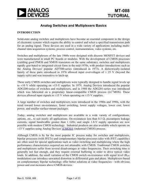
MT-088: Analog Switches and Multiplexers Basics
MT-088: Analog Switches and Multiplexers Basics
MT-088: Analog Switches and Multiplexers Basics

You also want an ePaper? Increase the reach of your titles
YUMPU automatically turns print PDFs into web optimized ePapers that Google loves.
<strong>MT</strong>-<strong>088</strong><br />
TUTORIAL<br />
<strong>Analog</strong> <strong>Switches</strong> <strong>and</strong> <strong>Multiplexers</strong> <strong>Basics</strong><br />
INTRODUCTION<br />
Solid-state analog switches <strong>and</strong> multiplexers have become an essential component in the design<br />
of electronic systems which require the ability to control <strong>and</strong> select a specified transmission path<br />
for an analog signal. These devices are used in a wide variety of applications including multichannel<br />
data acquisition systems, process control, instrumentation, video systems, etc.<br />
<strong>Switches</strong> <strong>and</strong> multiplexers of the late 1960s were designed with discrete MOSFET devices <strong>and</strong><br />
were manufactured in small PC boards or modules. With the development of CMOS processes<br />
(yielding good PMOS <strong>and</strong> NMOS transistors on the same substrate), switches <strong>and</strong> multiplexers<br />
rapidly gravitated to integrated circuit form in the mid-1970s, with product introductions such as<br />
the <strong>Analog</strong> Devices' popular AD7500-series (introduced in 1973). A dielectrically-isolated<br />
family of these parts introduced in 1976 allowed input overvoltages of ± 25 V (beyond the<br />
supply rails) <strong>and</strong> was insensitive to latch-up.<br />
These early CMOS switches <strong>and</strong> multiplexers were typically designed to h<strong>and</strong>le signal levels up<br />
to ±10 V while operating on ±15-V supplies. In 1979, <strong>Analog</strong> Devices introduced the popular<br />
ADG200-series of switches <strong>and</strong> multiplexers, <strong>and</strong> in 1988 the ADG201-series was introduced<br />
which was fabricated on a proprietary linear-compatible CMOS process (LC 2 MOS). These<br />
devices allowed input signals to ±15 V when operating on ±15-V supplies.<br />
A large number of switches <strong>and</strong> multiplexers were introduced in the 1980s <strong>and</strong> 1990s, with the<br />
trend toward lower on-resistance, faster switching, lower supply voltages, lower cost, lower<br />
power, <strong>and</strong> smaller surface-mount packages.<br />
Today, analog switches <strong>and</strong> multiplexers are available in a wide variety of configurations,<br />
options, etc., to suit nearly all applications. On-resistances less than 0.5 Ω, picoampere leakage<br />
currents, signal b<strong>and</strong>widths greater than 1 GHz, <strong>and</strong> single 1.8-V supply operation are now<br />
possible with modern CMOS technology. Industrial products are also available which operate on<br />
±15 V supplies using <strong>Analog</strong> Devices' iCMOS® (industrial CMOS) process.<br />
Although CMOS is by far the most popular IC process today for switches <strong>and</strong> multiplexers,<br />
bipolar processes (with JFETs) <strong>and</strong> complementary bipolar processes (also with JFET capability)<br />
are often used for special applications such as video switching <strong>and</strong> multiplexing where the high<br />
performance characteristics required are not attainable with CMOS. Traditional CMOS switches<br />
<strong>and</strong> multiplexers suffer from several disadvantages at video frequencies. Their switching time is<br />
generally not fast enough, <strong>and</strong> they require external buffering in order to drive typical video<br />
loads. In addition, the small variation of the CMOS switch on-resistance with signal level (R ON<br />
modulation) can introduce unwanted distortion in differential gain <strong>and</strong> phase. <strong>Multiplexers</strong> based<br />
on complementary bipolar technology offer better solutions at video frequencies—with obvious<br />
power <strong>and</strong> cost increases above CMOS devices.<br />
Rev.0, 10/08, WK Page 1 of 23
<strong>MT</strong>-<strong>088</strong><br />
CMOS SWITCH BASICS<br />
The ideal analog switch has no on-resistance, infinite off-impedance <strong>and</strong> zero time delay, <strong>and</strong><br />
can h<strong>and</strong>le large signal <strong>and</strong> common-mode voltages. Real CMOS analog switches meet none of<br />
these criteria, but if we underst<strong>and</strong> the limitations of analog switches, most of these limitations<br />
can be overcome.<br />
CMOS switches have an excellent combination of attributes. In its most basic form, the<br />
MOSFET transistor is a voltage-controlled resistor. In the "on" state, its resistance can be less<br />
than 1 Ω, while in the "off" state, the resistance increases to several hundreds of megohms, with<br />
picoampere leakage currents. CMOS technology is compatible with logic circuitry <strong>and</strong> can be<br />
densely packed in an IC. Its fast switching characteristics are well controlled with minimum<br />
circuit parasitics.<br />
MOSFET transistors are bilateral. That is, they can switch positive <strong>and</strong> negative voltages <strong>and</strong><br />
conduct positive <strong>and</strong> negative currents with equal ease. A MOSFET transistor has a voltage<br />
controlled resistance which varies nonlinearly with signal voltage as shown in Figure 1.<br />
PMOS<br />
NMOS<br />
ALTERNATE SYMBOLS<br />
Figure 1: MOSFET Switch ON-Resistance Versus Signal Voltage<br />
The complementary-MOS process (CMOS) yields good P-channel <strong>and</strong> N-channel MOSFETs.<br />
Connecting the PMOS <strong>and</strong> NMOS devices in parallel forms the basic bilateral CMOS switch of<br />
Figure 2. This combination reduces the on-resistance, <strong>and</strong> also produces a resistance which<br />
varies much less with signal voltage.<br />
Page 2 of 23
<strong>MT</strong>-<strong>088</strong><br />
SWITCH<br />
DRIVER<br />
SWITCH<br />
Figure 2: Basic CMOS Switch Uses Complementary Pair to<br />
Minimize R ON Variation due to Signal Swings<br />
Figure 3 shows the on-resistance changing with channel voltage for both N-type <strong>and</strong> P-type<br />
devices. This nonlinear resistance can causes errors in dc accuracy as well as ac distortion. The<br />
bilateral CMOS switch solves this problem. On-resistance is minimized, <strong>and</strong> linearity is also<br />
improved. The bottom curve of Figure 3 shows the improved flatness of the on-resistance<br />
characteristic of the switch.<br />
COMBINED TRANSFER<br />
FUNCTION<br />
Figure 3: CMOS Switch ON-Resistance Versus Signal Voltage<br />
The ADG8xx-series of CMOS switches are specifically designed for less than 0.5 Ω onresistance<br />
<strong>and</strong> are fabricated on a sub-micron process. These devices can carry currents up to 400<br />
mA, operate on a single 1.8 V to 5.5 V supply (depending on the particular device), <strong>and</strong> are rated<br />
over an extended temperature range of –40°C to +125°C. Typical on-resistance over temperature<br />
<strong>and</strong> input signal level is shown in Figure 4.<br />
Page 3 of 23
<strong>MT</strong>-<strong>088</strong><br />
INPUT SIGNAL LEVEL - V<br />
Figure 4: ON-Resistance Versus Input Signal for<br />
ADG801/ADG802 CMOS Switch, V DD = +5 V<br />
ERROR SOURCES IN THE BASIC CMOS SWITCH<br />
It is important to underst<strong>and</strong> the error sources in an analog switch. Many affect ac <strong>and</strong> dc<br />
performance, while others only affect ac. Figure 5 shows the equivalent circuit of two adjacent<br />
CMOS switches. The model includes leakage currents <strong>and</strong> junction capacitances.<br />
Figure 5: Equivalent Circuit of Two Adjacent CMOS <strong>Switches</strong><br />
Page 4 of 23
<strong>MT</strong>-<strong>088</strong><br />
DC errors associated with a single CMOS switch in the on state are shown in Figure 6. When the<br />
switch is on, dc performance is affected mainly by the switch on-resistance (R ON ) <strong>and</strong> leakage<br />
current (I LKG ). A resistive attenuator is created by the R G -R ON -R LOAD combination which<br />
produces a gain error. The leakage current, I LKG , flows through the equivalent resistance of<br />
R LOAD in parallel with the sum of R G <strong>and</strong> R ON .<br />
Not only can R ON cause gain errors—which can be calibrated using a system gain trim—but its<br />
variation with applied signal voltage (R ON modulation) can introduce distortion—for which there<br />
is no calibration. Low resistance circuits are more subject to errors due to R ON , while high<br />
resistance circuits are affected by leakage currents. Figure 6 also gives equations that show how<br />
these parameters affect dc performance.<br />
Figure 6: Factors Affecting DC Performance for<br />
ON Switch Condition: R ON , R LOAD , <strong>and</strong> I LKG<br />
When the switch is OFF, leakage current can introduce errors as shown in Figure 7. The leakage<br />
current flowing through the load resistance develops a corresponding voltage error at the output.<br />
Leakage current creates error voltage at V OUT equal to:<br />
V OUT = I LKG × R LOAD<br />
Figure 7: Factors Affecting DC Performance for<br />
OFF Switch Condition: I LKG <strong>and</strong> R LOAD<br />
Page 5 of 23
<strong>MT</strong>-<strong>088</strong><br />
Figure 8 illustrates the parasitic components that affect the ac performance of CMOS switches.<br />
Additional external capacitances will further degrade performance. These capacitances affect<br />
feedthrough, crosstalk <strong>and</strong> system b<strong>and</strong>width. C DS (drain-to-source capacitance), C D (drain-toground<br />
capacitance), <strong>and</strong> C LOAD all work in conjunction with R ON <strong>and</strong> R LOAD to form the overall<br />
transfer function.<br />
Figure 8: Dynamic Performance Considerations:<br />
Transfer Accuracy Versus Frequency<br />
In the equivalent circuit, C DS creates a frequency zero in the numerator of the transfer function<br />
A(s). This zero usually occurs at high frequencies because the switch on-resistance is small. The<br />
b<strong>and</strong>width is also a function of the switch output capacitance in combination with C DS <strong>and</strong> the<br />
load capacitance. This frequency pole appears in the denominator of the equation.<br />
The composite frequency domain transfer function may be re-written as shown in Figure 9 which<br />
shows the overall Bode plot for the switch in the on state. In most cases, the pole breakpoint<br />
frequency occurs first because of the dominant effect of the output capacitance C D . Thus, to<br />
maximize b<strong>and</strong>width, a switch should have low input <strong>and</strong> output capacitance <strong>and</strong> low onresistance.<br />
The series-pass capacitance, C DS , not only creates a zero in the response in the ON-state, it<br />
degrades the feedthrough performance of the switch during its OFF state. When the switch is off,<br />
C DS couples the input signal to the output load as shown in Figure 10.<br />
Page 6 of 23
<strong>MT</strong>-<strong>088</strong><br />
Figure 9: Bode Plot of CMOS Switch Transfer<br />
Function in the ON State<br />
Figure 9: Bode Plot of CMOS Switch Transfer<br />
Function in the ON State<br />
OFF Isolation is Affected<br />
by External R <strong>and</strong> C Load<br />
Figure 10: Dynamic Performance Considerations: Off Isolation<br />
Large values of C DS will produce large values of feedthrough, proportional to the input<br />
frequency. Figure 11 illustrates the drop in OFF-isolation as a function of frequency. The<br />
simplest way to maximize the OFF-isolation is to choose a switch that has as small a C DS as<br />
possible.<br />
Page 7 of 23
<strong>MT</strong>-<strong>088</strong><br />
Figure 11: Off Isolation Versus Frequency<br />
Figure 12 shows typical CMOS analog switch OFF-isolation as a function of frequency for the<br />
ADG708 8-channel multiplexer. From dc to several kilohertz, the multiplexer has nearly 90-dB<br />
isolation. As the frequency increases, an increasing amount of signal reaches the output.<br />
However, even at 10 MHz, the switch shown still has nearly 60 dB of isolation.<br />
Figure 12: OFF-Isolation Versus Frequency for<br />
ADG708 8-Channel Multiplexer<br />
Page 8 of 23
<strong>MT</strong>-<strong>088</strong><br />
Another ac parameter that affects system performance is the charge injection that takes place<br />
during switching. Figure 13 shows the equivalent circuit of the charge injection mechanism.<br />
V DD<br />
V SS<br />
Step waveforms of ± (V DD –V SS ) are applied to C Q ,<br />
the gate capacitance of the output switches.<br />
Figure 13: Dynamic Performance Considerations:<br />
Charge Injection Model<br />
When the switch control input is asserted, it causes the control circuit to apply a large voltage<br />
change (from V DD to V SS , or vice versa) at the gate of the CMOS switch. This fast change in<br />
voltage injects a charge into the switch output through the gate-drain capacitance C Q . The<br />
amount of charge coupled depends on the magnitude of the gate-drain capacitance.<br />
The charge injection introduces a step change in output voltage when switching as shown in<br />
Figure 14. The change in output voltage, ΔV OU T, is a function of the amount of charge injected,<br />
Q INJ (which is in turn a function of the gate-drain capacitance, C Q ) <strong>and</strong> the load capacitance, C L .<br />
0V<br />
Figure 14: Effects of Charge Injection on Output<br />
Page 9 of 23
<strong>MT</strong>-<strong>088</strong><br />
Another problem caused by switch capacitance is the retained charge when switching channels.<br />
This charge can cause transients in the switch output, <strong>and</strong> Figure 15 illustrates the phenomenon.<br />
Assume that initially S2 is closed <strong>and</strong> S1 open. C S1 <strong>and</strong> C S2 are charged to –5 V. As S2 opens,<br />
the –5 V remains on C S1 <strong>and</strong> C S2 , as S1 closes. Thus, the output of Amplifier A sees a –5V<br />
transient. The output will not stabilize until Amplifier A's output fully discharges C S1 <strong>and</strong> C S2<br />
<strong>and</strong> settles to 0 V. The scope photo in Figure 16 depicts this transient. The amplifier's transient<br />
load settling characteristics will therefore be an important consideration when choosing the right<br />
input buffer.<br />
–5V<br />
Figure 15: Charge Coupling Causes Dynamic Settling Time<br />
Transient When Multiplexing Signals<br />
Figure 16: Output of Amplifier Shows Dynamic Settling Time<br />
Transient Due to Charge Coupling<br />
Page 10 of 23
<strong>MT</strong>-<strong>088</strong><br />
Crosstalk is related to the capacitances between two switches. This is modeled as the C SS<br />
capacitance shown in Figure 17.<br />
Figure 17: Channel-to-Channel Crosstalk Equivalent<br />
Circuit for Adjacent <strong>Switches</strong><br />
Figure 18 shows typical crosstalk performance of the ADG708 8-channel CMOS multiplexer.<br />
Figure 18: Crosstalk Versus Frequency for ADG708 8-Channel Multiplexer<br />
Finally, the switch itself has a settling time that must be considered. Figure 19 shows the<br />
dynamic transfer function. The settling time can be calculated, because the response is a function<br />
of the switch <strong>and</strong> circuit resistances <strong>and</strong> capacitances. One can assume that this is a single-pole<br />
Page 11 of 23
<strong>MT</strong>-<strong>088</strong><br />
system <strong>and</strong> calculate the number of time constants required to settle to the desired system<br />
accuracy as shown in Figure 20.<br />
Settling time is the time required for the switch output<br />
to settle within a given error b<strong>and</strong> of the final value.<br />
Figure 19: Multiplexer Settling Time<br />
RESOLUTION,<br />
# OF BITS<br />
LSB (%FS)<br />
# OF TIME<br />
CONSTANTS<br />
6 1.563 4.16<br />
8 0.391 5.55<br />
10 0.0977 6.93<br />
12 0.0244 8.32<br />
14 0.0061 9.70<br />
16 0.00153 11.09<br />
18 0.00038 12.48<br />
20 0.000095 13.86<br />
22 0.000024 15.25<br />
Figure 20: Number of Time Constants Required to Settle to<br />
1 LSB Accuracy for a Single-Pole System<br />
Page 12 of 23
<strong>MT</strong>-<strong>088</strong><br />
APPLYING THE ANALOG SWITCH<br />
Switching time is an important consideration in applying analog switches, but switching time<br />
should not be confused with settling time. ON <strong>and</strong> OFF times are simply a measure of the<br />
propagation delay from the control input to the toggling of the switch, <strong>and</strong> are largely caused by<br />
time delays in the drive <strong>and</strong> level-shift circuits (see Figure 21). The t ON <strong>and</strong> t OFF values are<br />
generally measured from the 50% point of the control input leading edge to the 90% point of the<br />
output signal level.<br />
t ON , t OFF<br />
<br />
t ON <strong>and</strong> t OFF should not be confused with settling time.<br />
<br />
<br />
t ON <strong>and</strong> t OFF are simply a measure of the propagation delay<br />
from control input to operation of the analog switch. It is caused<br />
by time delays in the drive / level-shifter logic circuitry.<br />
t ON <strong>and</strong> t OFF are measured from the 50% point of the control<br />
input to the 90% point of the output signal level.<br />
Figure 21: Applying the <strong>Analog</strong> Switch: Dynamic<br />
Performance Considerations<br />
We will next consider the issues involved in buffering a CMOS switch or multiplexer output<br />
using an op amp. When a CMOS multiplexer switches inputs to an inverting summing amplifier,<br />
it should be noted that the on-resistance, <strong>and</strong> its nonlinear change as a function of input voltage,<br />
will cause gain <strong>and</strong> distortion errors as shown in Figure 22. If the resistors are large, the switch<br />
leakage current may introduce error. Small resistors minimize leakage current error but increase<br />
the error due to the finite value of R ON .<br />
Page 13 of 23
<strong>MT</strong>-<strong>088</strong><br />
10kΩ<br />
10kΩ<br />
ΔV SWITCH = ±10V<br />
<br />
<br />
ΔR ON caused by ΔV IN , degrades linearity of V OUT relative to V IN .<br />
ΔR ON causes overall gain error in V OUT relative to V IN .<br />
Figure 22: Applying the <strong>Analog</strong> Switch: Unity<br />
Gain Inverter with Switched Input<br />
To minimize the effect of R ON change due to the change in input voltage, it is advisable to put<br />
the multiplexing switches at the op amp summing junction as shown in Figure 23. This ensures<br />
the switches are only modulated with about ±100 mV rather than the full ±10 V—but a separate<br />
resistor is required for each input leg.<br />
10kΩ<br />
10kΩ<br />
10kΩ<br />
10kΩ<br />
10kΩ<br />
ΔV SWITCH = ±100mV<br />
<br />
<br />
Switch drives a virtual ground.<br />
Switch sees only ±100mV, not ±10V, minimizes ΔR ON .<br />
Figure 23: Applying the <strong>Analog</strong> Switch:<br />
Minimizing the Influence of ΔR ON<br />
Page 14 of 23
<strong>MT</strong>-<strong>088</strong><br />
It is important to know how much parasitic capacitance has been added to the summing junction<br />
as a result of adding a multiplexer, because any capacitance added to that node introduces phase<br />
shift to the amplifier closed loop response. If the capacitance is too large, the amplifier may<br />
become unstable <strong>and</strong> oscillate. A small capacitance, C 1 , across the feedback resistor may be<br />
required to stabilize the circuit.<br />
The finite value of R ON can be a significant error source in the circuit shown in Figure 24. The<br />
gain-setting resistors should be at least 1,000 times larger than the switch on-resistance to<br />
guarantee 0.1% gain accuracy. Higher values yield greater accuracy but lower b<strong>and</strong>width <strong>and</strong><br />
greater sensitivity to leakage <strong>and</strong> bias current.<br />
A better method of compensating for R ON is to place one of the switches in series with the<br />
feedback resistor of the inverting amplifier as shown in Figure 25. It is a safe assumption that the<br />
multiple switches, fabricated on a single chip, are well-matched in absolute characteristics <strong>and</strong><br />
tracking over temperature. Therefore, the amplifier is closed-loop gain stable at unity gain, since<br />
the total feedforward <strong>and</strong> feedback resistors are matched.<br />
1MΩ<br />
1MΩ<br />
<br />
<br />
<br />
<br />
ΔR ON is small compared to 1MΩ switch load.<br />
Effect on transfer accuracy is minimized.<br />
Bias current <strong>and</strong> leakage current effects are now very important.<br />
Circuit b<strong>and</strong>width degrades.<br />
Figure 24: Applying the <strong>Analog</strong> Switch: Minimizing Effects<br />
of ΔR ON Using Large Resistor Values<br />
Page 15 of 23
<strong>MT</strong>-<strong>088</strong><br />
R F<br />
10kΩ<br />
±10V<br />
±10V<br />
±10V<br />
10kΩ<br />
10kΩ<br />
10kΩ<br />
Figure 25: Applying the <strong>Analog</strong> Switch:Using "Dummy" Switch<br />
in Feedback to Minimize Gain Error Due to ΔR ON<br />
The best multiplexer design drives the non-inverting input of the amplifier as shown in Figure<br />
26. The high input impedance of the non-inverting input eliminates the errors due to R ON .<br />
Figure 26: Applying the <strong>Analog</strong> Switch: Minimizing the Influence of ΔR ON<br />
Using Non-Inverting Configuration<br />
CMOS switches <strong>and</strong> multiplexers are often used with op amps to make programmable gain<br />
amplifiers (PGAs). To underst<strong>and</strong> R ON 's effect on their performance, consider Figure 27, a poor<br />
PGA design. A non-inverting op amp has 4 different gain-set resistors, each grounded by a<br />
switch, with an R ON of 100-500 Ω. Even with R ON as low as 25 Ω, the gain of 16 error would be<br />
2.4%, worse than 8-bit accuracy! R ON also changes over temperature, <strong>and</strong> from switch-to-switch.<br />
Page 16 of 23
<strong>MT</strong>-<strong>088</strong><br />
R F = 10kΩ<br />
–<br />
625Ω 1.43kΩ 3.33kΩ 10kΩ<br />
G = 16 G = 8 G = 4 G = 2<br />
+<br />
V OUT<br />
V IN<br />
<br />
<br />
<br />
<br />
<br />
Gain accuracy limited by switch's on-resistance R ON<br />
<strong>and</strong> R ON modulation<br />
R ON typically 1 - 500Ω for CMOS or JFET switch<br />
For R ON = 25Ω, there is a 2.4% gain error for G = 16<br />
R ON drift over temperature limits accuracy<br />
Must use very low R ON switches<br />
Figure 27: A Poorly Designed PGA Using CMOS <strong>Switches</strong><br />
To attempt "fixing" this design, the resistors might be increased, but noise <strong>and</strong> offset could then<br />
be a problem. The only way to improve accuracy with this circuit is to use relays, with virtually<br />
no R ON . Only then will the few mΩ of relay R ON be a small error vis-à-vis 625 Ω.<br />
It is much better to use a circuit insensitive to R ON ! In Figure 28, the switch is placed in series<br />
with the inverting input of an op amp. Since the op amp input impedance is very large, the switch<br />
R ON is now irrelevant, <strong>and</strong> gain is now determined solely by the external resistors. Note—R ON<br />
may add a small offset error if op amp bias current is high. If this is the case, it can readily be<br />
compensated with an equivalent resistance at V IN .<br />
V IN<br />
+<br />
V OUT<br />
–<br />
G = 1<br />
500Ω<br />
G = 2<br />
1kΩ<br />
1kΩ<br />
<br />
<br />
<br />
R ON is not in series with gain setting resistors<br />
R ON is small compared to input impedance<br />
Only slight offset errors occur due to bias<br />
current flowing through the switches<br />
Figure 28: Alternate PGA Configuration Minimizes the Effects of R ON<br />
Page 17 of 23
<strong>MT</strong>-<strong>088</strong><br />
1-GHz CMOS SWITCHES<br />
The ADG918/ADG919 are the first switches using a CMOS process to provide high isolation<br />
<strong>and</strong> low insertion loss up to <strong>and</strong> exceeding 1 GHz. The switches exhibit low insertion loss (0.8<br />
dB) <strong>and</strong> relatively high off isolation (37 dB) when transmitting a 1-GHz signal. In high<br />
frequency applications with throughput power of +18 dBm or less at 25°C, they are a costeffective<br />
alternative to gallium arsenide (GaAs) switches. A block diagram of the devices are<br />
shown in Figure 29 along with isolation <strong>and</strong> loss versus frequency plots given in Figure 30.<br />
ABSORPTIVE SWITCH<br />
REFLECTIVE SWITCH<br />
Figure 29: 1-GHz CMOS 1.65-V to 2.75-V 2:1 Mux/SPDT <strong>Switches</strong><br />
ISOLATION (dB) VS. FREQUENCY<br />
LOSS (dB)VS. FREQUENCY<br />
Figure 30: Isolation <strong>and</strong> Frequency Response of<br />
AD918/AD919 1-GHz Switch<br />
Page 18 of 23
<strong>MT</strong>-<strong>088</strong><br />
The ADG918 is an absorptive switch with 50-Ω terminated shunt legs that allow impedance<br />
matching with the application circuit, while the ADG919 is a reflective switch designed for use<br />
where the terminations are external to the chip. Both offer low power consumption (
<strong>MT</strong>-<strong>088</strong><br />
+V DD<br />
–V SS<br />
Figure 32: Bipolar Transistor Equivalent Circuit for CMOS<br />
Switch Shows Parasitic SCR Latch<br />
In general, to prevent the latchup condition, the inputs to CMOS devices should never be<br />
allowed to be more than 0.3 V above the positive supply or 0.3 V below the negative supply.<br />
Note that this restriction also applies when the power supplies are off (V DD = V SS = 0 V), <strong>and</strong><br />
therefore devices can latchup if power is applied to a part when signals are present on the inputs.<br />
Manuracturers of CMOS devices invariably place this restriction in the data sheet table of<br />
absolute maximum ratings. In addition, the input current under overvoltage conditions should be<br />
restricted to 5-30 mA, depending upon the particular device.<br />
In order to prevent this type of SCR latchup, a series diode can be inserted into the V DD <strong>and</strong> V SS<br />
terminals as shown in Figure 33. The diodes block the SCR gate current. Normally the parasitic<br />
transistors Q1 <strong>and</strong> Q2 have low beta (usually less than 10) <strong>and</strong> require a comparatively large gate<br />
current to fire the SCR. The diodes limit the reverse gate current so that the SCR is not triggered.<br />
CR1<br />
+V DD –V SS<br />
CR2<br />
Diodes CR1 <strong>and</strong> CR2 block base current drive to Q1 <strong>and</strong> Q2<br />
in the event of overvoltage at S or D.<br />
Figure 33: Diode Protection Scheme for CMOS Switch<br />
Page 20 of 23
<strong>MT</strong>-<strong>088</strong><br />
If diode protection is used, the analog voltage range of the switch will be reduced by one V BE<br />
drop at each rail, <strong>and</strong> this can be inconvenient when using low supply voltages.<br />
As noted, CMOS switches <strong>and</strong> multiplexers can also be protected from possible overcurrent by<br />
inserting a series resistor to limit the current to a safe level as shown in Figure 34, generally less<br />
than 5-30 mA. Because of the resitive attenuator formed by R LOAD <strong>and</strong> R LIMIT , this method works<br />
only if the switch drives a relatively high impedance load.<br />
+V DD<br />
CMOS SWITCH<br />
OR MUX<br />
INPUT<br />
R LIMIT<br />
OUTPUT<br />
R LOAD<br />
LIMIT OVERCURRENT TO 5-30mA<br />
–V SS<br />
Figure 34: Overcurrent Protection Using External Resistor<br />
A common method for input protection is shown in Figure 35 where Schottky diodes are<br />
connected from the input terminal to each supply voltage as shown. The diodes effectively<br />
prevent the inputs from exceeding the supply voltage by more than 0.3-0.4 V, thereby preventing<br />
latchup conditions. In addition, if the input voltage exceeds the supply voltage, the input current<br />
flows through the external diodes to the supplies, not the device. Schottky diodes can easily<br />
h<strong>and</strong>le 50-100 mA of transient current, therefore the R LIMIT resistor can be quite low.<br />
+V DD<br />
INPUT<br />
R LIMIT<br />
CMOS SWITCH<br />
OR MUX<br />
OUTPUT<br />
R LOAD<br />
–V SS<br />
Figure 35: Input Protection Using External Schottky Diodes<br />
Page 21 of 23
<strong>MT</strong>-<strong>088</strong><br />
REFERENCES:<br />
1. Hank Zumbahlen, Basic Linear Design, <strong>Analog</strong> Devices, 2006, ISBN: 0-915550-28-1. Also available as<br />
Linear Circuit Design H<strong>and</strong>book, Elsevier-Newnes, 2008, ISBN-10: 0750687037, ISBN-13: 978-<br />
0750687034. Chapter 7.<br />
2. Walt Kester, <strong>Analog</strong>-Digital Conversion, <strong>Analog</strong> Devices, 2004, ISBN 0-916550-27-3, Chapter 7. Also<br />
available as The Data Conversion H<strong>and</strong>book, Elsevier/Newnes, 2005, ISBN 0-7506-7841-0, Chapter 7.<br />
Copyright 2009, <strong>Analog</strong> Devices, Inc. All rights reserved. <strong>Analog</strong> Devices assumes no responsibility for customer<br />
product design or the use or application of customers’ products or for any infringements of patents or rights of others<br />
which may result from <strong>Analog</strong> Devices assistance. All trademarks <strong>and</strong> logos are property of their respective holders.<br />
Information furnished by <strong>Analog</strong> Devices applications <strong>and</strong> development tools engineers is believed to be accurate<br />
<strong>and</strong> reliable, however no responsibility is assumed by <strong>Analog</strong> Devices regarding technical accuracy <strong>and</strong> topicality of<br />
the content provided in <strong>Analog</strong> Devices Tutorials.<br />
Page 23 of 23