technical manual for sailor compact hf ssb t2130 - Gopher Proxy
technical manual for sailor compact hf ssb t2130 - Gopher Proxy
technical manual for sailor compact hf ssb t2130 - Gopher Proxy

You also want an ePaper? Increase the reach of your titles
YUMPU automatically turns print PDFs into web optimized ePapers that Google loves.
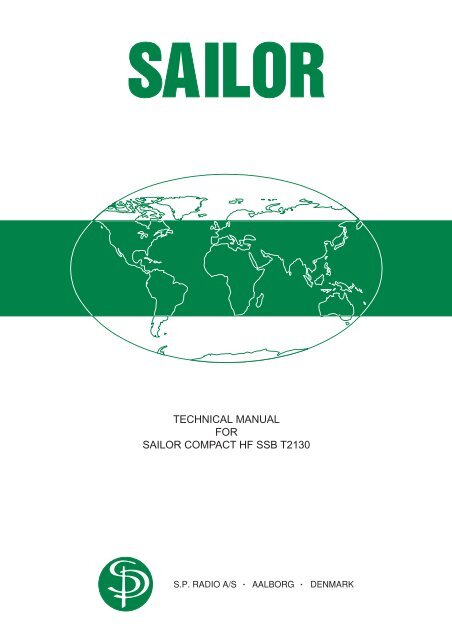
TECHNICAL MANUAL<br />
FOR<br />
SAILOR COMPACT HF SSB T2130<br />
S.P. RADIO A/S AALBORG DENMARK
Please note<br />
Any responsibility or liability <strong>for</strong> loss or damage in connection with the use of this product and the<br />
accompanying documentation is disclaimed.<br />
The in<strong>for</strong>mation in this <strong>manual</strong> is furnished <strong>for</strong> in<strong>for</strong>mational use only, is subject to change without<br />
notice, may contain errors or inaccuracies, and represents no commitment whatsoever.<br />
This agreement is governed by the laws of Denmark.<br />
Doc. no.: M2130GB Issue: A/0129
T2130<br />
CONTENTS<br />
1 GENERAL INFORMATION<br />
1.1 INTRODUCTION 1-1<br />
1.2 GENERAL DESCRIPTION 1-1<br />
1.3 TECHNICAL DATA 1-2<br />
1.4 PRINCIPLE OF OPERATION AND BLOCK DIAGRAM 1-4<br />
2 INSTALLATION MECHANICAL HF SSB TRANSMITTER T2130<br />
2.1 MOUNTING POSSIBILITIES/DIMENSIONS AND DRILLING PLAN 2-1<br />
2.1.1 INSTALLATION HINTS 2-4<br />
2.2.2 BATTERY REQUIREMENTS FOR GMDSS 2-5<br />
2.2.3 AERIAL AND RF GROUNDING REQUIREMENTS 2-7<br />
2.2.4 MAIN CABLE PLANE WHEN SUPPLIED FROM 24V BATTERY. 2-11<br />
2.2.5 MAIN CABLE PLANE WHEN SUPPLIED FROM 12V DC BATTERY,<br />
USING N2160 12V DC TO 24 V DC CONVERTER. 2-12<br />
2.2.6 MAIN CABLE PLAN WHEN SUPPLIED FROM AC,<br />
USING N2161 AC TO 24V DC POWER SUPPLY.<br />
MAIN CABLE PLAN WHEN SUPPLIED BOTH FROM AC<br />
AND DC (N2161). 2-13<br />
2.2.7 INSTALLATION WITH REMOTE CONTROL C2140 2-14<br />
2.2.8 INSTALLATION WITH DSC (TELEX) RM2150 2-16<br />
2.2.10 CONNECTIONS TO T2130 2-17<br />
2.2.11 CONNECTIONS TO RE2100 2-18<br />
2.2.12 CONNECTIONS TO AT2110 2-19<br />
2.2.13 CONNECTIONS TO N2161 2-20<br />
2.2.14 CONNECTIONS TO BATTERY CHARGER N2174 2-21<br />
2.3 SYSTEM DESCRIPTION AND TROUBLE SHOOTING 2-23<br />
2.3.3 SYSTEM FUNCTIONAL DESCRIPTION 2-24<br />
9724<br />
3 SERVICE<br />
3.1 MAINTENANCE 3-1<br />
3.2 ALIGNMENT INSTRUCTIONS 3-1<br />
3.3 PROPOSAL FOR NECESSARY MEASURING INSTRUMENTS 3-1<br />
3.4 TROUBLE SHOOTING 3-2<br />
3.4.1 POWER AMPLIFIER (MODULE 1) 3-5<br />
3.4.2 OUTPUT FILTER (MODULE 2) 3-6<br />
3.4.3 TX-PROCESSOR (MODULE 3) 3-7<br />
3.4.4 POWER SUPPLY (MODULE 4) 3-8<br />
3.4.5 NOT USED 3-10<br />
3.4.6 CONNECTION BOARD (MODULE 6) 3-10<br />
3.4.7 REPLACEMENT OF COMPONENTS 3-10<br />
3.4.8 REPLACEMENT OF MODULES 3-10<br />
3.5 PERFORMANCE CHECK 3-11<br />
3.5.1 POWER AMPLIFIER (MODULE 1) 3-12<br />
3.5.2 OUTPUT FILTER (MODULE 2) 3-13<br />
3.5.3 TX-PROCESSOR (MODULE 3) 3-14<br />
3.5.4 POWER SUPPLY (MODULE 4) 3-19<br />
3.5.5 NOT USED 3-20<br />
3.5.6 CONNECTION BOARD (MODULE 6) 3-20<br />
3.6 ADJUSTMENT PROCEDURE 3-21<br />
3.6.1 POWER AMPLIFIER (MODULE 1) 3-21
T2130<br />
3.6.2 ADJUSTMENT OF OUTPUT FILTER (MODULE 2) 3-21<br />
3.6.3 ADJUSTMENT OF DRIVE LEVEL 3-21<br />
3.7 NECESSARY ADJUSTMENTS AFTER REPAIR 3-23<br />
3.7.1 MODULES REPLACED 3-23<br />
3.7.2 COMPONENTS REPLACED 3-24<br />
3.8 FUNCTION CHECK 3-25<br />
3.8.1 FUNCTION CHECK FOR THE TRANSMITTER INSTALLED 3-25<br />
3.8.3 BATTERY CHECK 3-25<br />
3.8.4 OUTPUT POWER CHECK 3-25<br />
3.8.5 SWR CHECK 3-25<br />
3.8.6 CHECK OF POWER GAIN IN PA-MODULE (1) 3-25<br />
3.8.7 END OF SERVICE PROGRAMME 3-25<br />
3.9 SERVICE PROGRAMMES 3-27<br />
3.9.1 SERVICE PROGRAMMES IN T2130 3-27<br />
3.9.2 SERVICE PROGRAMMES RELATED TO AT2110 3-32<br />
4 MECHANICAL DISASSEMBLING<br />
4.1 MECHANICAL DISASSEMBLING AND MODULE LOCATION 4-1<br />
5 CIRCUIT DESCRIPTION AND SCHEMATIC DIAGRAMS<br />
5.1 POWER AMPLIFIER (MODULE 1) PART NO. 625641 5-1<br />
5.2 OUTPUT FILTER (MODULE 2) PART NO. 625642 5-2<br />
5.3 TX-PROCESSOR (MODULE 3) PART NO. 625643 5-5<br />
5.4 POWER SUPPLY I (MODULE 4) PART NO. 625644 5-7<br />
5.6 COMPONENT LOCATION CONNECTION BOARD MODULE 6 5-28<br />
5.9 INTERCONNECTION CABLE PLAN 5-31<br />
6 PARTS LIST<br />
9724
T2130<br />
CONTENTS<br />
1 GENERAL INFORMATION<br />
1.1 INTRODUCTION 1-1<br />
1.2 GENERAL DESCRIPTION 1-1<br />
1.3 TECHNICAL DATA 1-2<br />
1.4 PRINCIPLE OF OPERATION AND BLOCK DIAGRAM 1-4<br />
9724
1 GENERAL INFORMATION T2130<br />
1 GENERAL INFORMATION<br />
1.1 INTRODUCTION<br />
The SAILOR Compact HF SSB T2130 is a 250W PEP SSB transmitter <strong>for</strong> the SAILOR Compact HF SSB<br />
Programme 2000.<br />
SAILOR Compact HF SSB Programme 2000 is a powerful, advanced, high technology short wave<br />
communication system, which is extremely easy to operate.<br />
Is has been developed on the basis of S. P. Radio’s many years of experience with short wave<br />
communication equipment.<br />
Is has the same high reliability as all SAILOR equipment is known <strong>for</strong>.<br />
SAILOR HF SSB PROGRAMME 2000 CONSISTS OF THE FOLLOWING UNITS:<br />
RE2100:<br />
Control unit with integral receiver and exciter.<br />
T2130: 250W PEP SSB transmitter with integral power supply <strong>for</strong> RE2100.<br />
Supply voltage 24V.<br />
AT2110:<br />
250W PEP aerial coupler <strong>for</strong> use outdoors.<br />
N2160: 12V DC power supply <strong>for</strong> T2130.<br />
N2161: 110/220/240V AC, 50 Hz power supply <strong>for</strong> T2130.<br />
1.2 GENERAL DESCRIPTION<br />
SAILOR HF SSB T2130 is an all solid state constructed microcomputer controlled SSB shortwave<br />
transmitter.<br />
SAILOR HF SSB T2130 covers the frequency range from 1.6 MHz to 30 MHz.<br />
SAILOR HF SSB T2130 has an output power of 250W PEP.<br />
SAILOR HF SSB T2130 is constructed <strong>for</strong> continuous operation.<br />
SAILOR HF SSB T2130 has 50 ohm output impedance.<br />
SAILOR HF SSB T2130 is able to control the automatic aerial coupler AT2110.<br />
SAILOR HF SSB T2130 has built-in power supply <strong>for</strong> 24V DC.<br />
SAILOR HF SSB T2130 is able to supply the transceiver RE2100.<br />
SAILOR HF SSB T2130 has built-in protection system, so that it will not be damaged if the aerial<br />
is open circuited or short-circuited.<br />
9345<br />
PAGE 1-1
1 GENERAL INFORMATION T2130<br />
1.3 TECHNICAL DATA<br />
(complies with SOLAS, ITU, CEPT, MPT, DOC, FTZ, KSR, FCC)<br />
GENERAL<br />
Frequency Range: Receiver: 100 kHz to 30 MHz<br />
Transmitter: 1.6 MHz to 30 MHz<br />
Modes:<br />
Channel Capacity:<br />
Scanning Facilities:<br />
Distress Call:<br />
J3E (USB/LSB), R3E and H3E (AM)<br />
100 user defined quick-select channels and ITU defined channels<br />
in the maritime bands. Each channel contains both RX and TX frequency<br />
and mode settings.<br />
10 scanning prograammes, each able to contain<br />
128 pairs of frequencies.<br />
Quick selection of 2182 kHz<br />
Built-in two tone alarm: 1300 Hz and 2200 Hz<br />
with a duration of 45 secs.<br />
Operating Temperature Range:<br />
-15°C to +55°C<br />
Frequency Stability:<br />
Better than 0.34 ppm<br />
Primary Voltage: 24V DC - 10% +30%<br />
Current Drain: Receiver (standby) 0.9A<br />
Transmit voice 7A<br />
Transmit two-tone 13A<br />
Aerials:<br />
from 7 - 15 m<br />
TRANSMITTER T2130<br />
Power Output:<br />
Intermodulation:<br />
Spurious Emission:<br />
Harmonics:<br />
Carrier Suppression:<br />
Audio Response:<br />
250W PEP ± 1.4 dB (T2130/I 240W PEP max.)<br />
better than 32 dB below PEP<br />
better than 67 dB below PEP<br />
better than 43 dB below PEP or<br />
better than 67 dB below PEP with aerial coupler AT2110<br />
better than 46 dB below PEP<br />
350 Hz to 2700 Hz at -6 dB<br />
RECEIVER RE2100<br />
Receive System:<br />
Selectivity:<br />
Double conversion super heterodyne<br />
1st IF 70 MHz. 2nd 10.73 MHz<br />
J3E (SSB) 350 Hz to 2700 Hz at -6 dB<br />
H3E (AM) ±3.3 kHz at -6 dB<br />
PAGE 1-2<br />
9345
1 GENERAL INFORMATION T2130<br />
Sensitivity:<br />
Spurious and IF Rejection:<br />
Cross Modulaton:<br />
Desensitization:<br />
AGC:<br />
Intermodulation:<br />
Spurious Emission:<br />
Clarifier:<br />
Squelch:<br />
J3E (SSB)
1 GENERAL INFORMATION T2130<br />
1.4 PRINCIPLE OF OPERATION AND BLOCK DIAGRAM<br />
SAILOR Compact HF SSB T2130 is a 250W PEP transmitter in SAILOR Compact HF SSB Programme<br />
2000. It contains following circuits.<br />
POWER AMPLIFIER<br />
The power amplifier is a push-pull amplifier.<br />
The input signal from RE2100 is fed through a TX/RX switch on the output filter unit to the input of the<br />
power amplifier. The signal is amplified to approx. 280W PEP. The bias to the pre-driver, driver, and PA<br />
can be switched off from the TX microprocessor. When this is done, the output power will be attenuated<br />
more than 60 dB.<br />
OUTPUT FILTER<br />
The output filter consists of six lowpass filters, a directional coupler, a tune/transmit switch, and a TX/RX<br />
switch.<br />
From the power amplifier the signal is fed to a lowpass filter, which attenuates all harmonics. Then the<br />
signal passes a directional coupler, which gives in<strong>for</strong>mation about the standing wave ratio to the TXprocessor<br />
unit.<br />
After the directional coupler the signal is fed to a drive/transmit switch. In position drive the output power<br />
is fed to a 50 ohm load. This load is used to set the output power to the correct value.<br />
After this switch the signal is fed to the TX/RX switch.<br />
In position RX the signal from the aerial coupler AT2110 or the aerial is fed directly to RE2100.<br />
In position TX the signal from RE2100 is fed to the input of the power amplifier and the output power is<br />
fed to the aerial coupler AT2110 or the aerial.<br />
TX PROCESSOR<br />
The processor takes care of controlling the power amplifier, output filters, aerial coupler AT2110, and<br />
communication with RE2100.<br />
From RE2100 the TX-processor receives in<strong>for</strong>mation about frequency and receive/transmit mode. The<br />
TX-processor gives in<strong>for</strong>mation to RE2100 about tuning/tune ready and attenuator setting.<br />
During tune-up the TX-processor is controlling the aerial coupler. It tunes <strong>for</strong> best standing wave ratio<br />
measured with the directional coupler on the output filter module.<br />
During transmit the TX-processor is checking the temperature of the PA-transistors, supply voltage, and<br />
stating wave ratio. From these data the TX processor calculates the max. permissible power, and then<br />
sends this in<strong>for</strong>mation to the RE2100, where the processor unit sets the attenuator in the exciter unit to<br />
the correct value.<br />
POWER SUPPLY<br />
This unit consists of two power supplies and the AF-amplifier.<br />
The 24V DC is first fed to a relay which switches off/on the supply to the power supplies.<br />
One switch mode power supply is used to generate ±18V and 9V <strong>for</strong> all small signal circuits in T2130 and<br />
RE2100. The supply <strong>for</strong> the power amplifier and the AF-amplifier passes through a serial regulator, which<br />
limits the voltage to max. 28V.<br />
PAGE 1-4<br />
9345
1 GENERAL INFORMATION T2130<br />
CONNECTION BOARD<br />
The connection board is the interface to the aerial coupler AT2110, HF SSB RE2100, 24V mains, and<br />
other units e.g. loudspeaker, muting of ext. receivers etc.<br />
All input and output from ext. equipment are made through an optocoupler, a relay, or a trans<strong>for</strong>mer.<br />
BLOCK DIAGRAM T2130<br />
25888B<br />
9345<br />
PAGE 1-5
T2130<br />
CONTENTS<br />
2 INSTALLATION MECHANICAL HF SSB TRANSMITTER T2130<br />
2.1 MOUNTING POSSIBILITIES/DIMENSIONS AND DRILLING PLAN 2-1<br />
2.1.1 INSTALLATION HINTS 2-4<br />
2.2.2 BATTERY REQUIREMENTS FOR GMDSS 2-5<br />
2.2.3 AERIAL AND RF GROUNDING REQUIREMENTS 2-7<br />
2.2.4 MAIN CABLE PLANE WHEN SUPPLIED FROM 24V BATTERY. 2-11<br />
2.2.5 MAIN CABLE PLANE WHEN SUPPLIED FROM 12V DC BATTERY,<br />
USING N2160 12V DC TO 24 V DC CONVERTER. 2-12<br />
2.2.6 MAIN CABLE PLAN WHEN SUPPLIED FROM AC,<br />
USING N2161 AC TO 24V DC POWER SUPPLY.<br />
MAIN CABLE PLAN WHEN SUPPLIED BOTH FROM AC<br />
AND DC (N2161). 2-13<br />
2.2.7 INSTALLATION WITH REMOTE CONTROL C2140 2-14<br />
2.2.8 INSTALLATION WITH DSC (TELEX) RM2150 2-16<br />
2.2.10 CONNECTIONS TO T2130 2-17<br />
2.2.11 CONNECTIONS TO RE2100 2-18<br />
2.2.12 CONNECTIONS TO AT2110 2-19<br />
2.2.13 CONNECTIONS TO N2161 2-20<br />
2.2.14 CONNECTIONS TO BATTERY CHARGER N2174 2-21<br />
2.3 SYSTEM DESCRIPTION AND TROUBLE SHOOTING 2-23<br />
2.3.3 SYSTEM FUNCTIONAL DESCRIPTION 2-24<br />
2.3.3.1 SP BUS COMMUNICATION TO T2130 2-24<br />
2.3.3.2 AUTOMATIC POWER SETTING 2-26<br />
2.3.3.3 TUNING THE AT2110 2-30<br />
2.3.3.4 TRANSMIT SUPERVISING 2-32<br />
2.3.3.5 CALIBRATION OF THE T2130 2-34<br />
9724
T2130<br />
2 INSTALLATION MECHANICAL HF SSB TRANSMITTER T2130<br />
2.1 MOUNTING POSSIBILITIES/DIMENSIONS AND DRILLING PLAN<br />
25889B<br />
9630<br />
PAGE 2-1
2 INSTALLATION MECHANICAL HF SSB TRANSMITTER T2130<br />
Free space <strong>for</strong> air circulation.<br />
Ambient temperature:<br />
Max. 40 o C.<br />
Weight: T2130: 14 kg<br />
Free space <strong>for</strong> air circulation<br />
and cable entry.<br />
25891A<br />
25890A<br />
PAGE 2-2<br />
9630
2 INSTALLATION MECHANICAL HF SSB TRANSMITTER T2130<br />
26197A<br />
9630<br />
PAGE 2-3
2 INSTALLATION MECHANICAL HF SSB TRANSMITTER T2130<br />
2.1.1 INSTALLATION HINTS<br />
The HF SSB Transmitter T2130 has to be installed vertically because it is convection cooled.<br />
To ensure free airflow inside the transmitter, at least 100 mm free space is necessary at the top<br />
of the cover. At the bottom of the transmitter, 100 mm free space is necessary <strong>for</strong> cable lead-in.<br />
In order to facilitate the installation, dismantle the turnable inner chassis (see the section 4.0.<br />
MECHANICAL DISASSEMBLING). Then install the back plate with the connection board PCB<br />
as described in section 2.1. MOUNTING POSSIBILITIES/DIMENSIONS AND DRILLING<br />
PLAN.<br />
When all cables have been connected according to the cable plans in question, reinstall the<br />
turnable inner chassis and complete the installation by executing the function check (see the<br />
section 3.8. FUNCTION CHECK).<br />
25958D<br />
PAGE 2-4<br />
9630
2 INSTALLATION MECHANICAL HF SSB TRANSMITTER T2130<br />
2.2.2 BATTERY REQUIREMENTS FOR GMDSS<br />
6 HOURS REQUIREMENT:<br />
The radio batteries must have sufficient capacity to supply the radio station <strong>for</strong> 6 hours (3 hours transmit<br />
and 3 hours standby).<br />
When the battery is drained in 6 hours, instead of the normal 20 hours, you have add 20% to the capacity<br />
given be the manufacture.<br />
The three hours transmit has to be in telex mode ARQ.<br />
Equipment Mode Current Battery capacity<br />
T2130/DSC transmit 15A 45Ah<br />
T2130/DSC standby 1A 3Ah<br />
VHF/DSC transmit 7A 21Ah<br />
VHF/DSC standby .33A 1Ah<br />
EMERGENCY LIGHT on 1A 6Ah<br />
GPS RECEIVER on 1A 6Ah<br />
TOTAL 6 HOURS<br />
82,0Ah<br />
+20% 98.4Ah<br />
If you chose to make a installation without AC power supply N2161. Then you must have a battery charger<br />
large enough to ensure, that you not will drain your batteries during transmission. That gives a charger<br />
requirement of 25 amp.The maximum allowable charge current is 10% of the battery capacity. When the<br />
charger can give 25 amps the battery capacity must be 250Ah.<br />
We recommend 250Ah battery capacity.<br />
If you chose to make a installation with AC and DC power supply N2161. Then you must have a battery<br />
charger large enough to ensure, that you can charge your batteries, within 10 hours. That gives a charger<br />
requirement of 10 amp.<br />
The maximum allowable charge current is 10% of the battery capacity.<br />
We recommend 100Ah battery capacity.<br />
9315<br />
PAGE 2-5
2 INSTALLATION MECHANICAL HF SSB TRANSMITTER T2130<br />
1 HOUR REQUIREMENT:<br />
The radio batteries must have sufficient capacity to supply the radio station <strong>for</strong> 1 hour (0.5 hours transmit<br />
and 0.5 hours standby).<br />
When the battery is drained in 1 hour, instead of the 24 hours, you have add 50% to the capacity given<br />
be the manufacture.<br />
The half hour transmit has to be in telex mode ARQ.<br />
Equipment Mode Current Battery capacity<br />
T2130/DSC transmit 15A 7.5Ah<br />
T2130/DSC standby 1A 0.5Ah<br />
VHF/DSC transmit 7A 3.5Ah<br />
VHF/DSC standby .33A .17Ah<br />
EMERGENCY LIGHT on 1A 1Ah<br />
GPS RECEIVER on 1A 1Ah<br />
TOTAL 1 HOURS<br />
13.7Ah<br />
+50% 20.6Ah<br />
If you chose to make a installation without AC power supply N2161. Then you must have a battery charger<br />
large enough to ensure, that you not will drain your batteries during transmission. That gives a charger<br />
requirement of 25 amp.<br />
The maximum allowable charge current is 10% of the battery capacity. When the charger can give 25<br />
amps the battery capacity must be 250Ah.<br />
We recommend 250Ah battery capacity.<br />
If you chose to make a installation with AC and DC power supply N2161. Then you must have a battery<br />
charger large enough to ensure, that you can charge your batteries within 10 hours. That gives a charger<br />
requirement of 3 amp.<br />
The maximum allowable charge current is 10% of the battery capacity.<br />
We recommend 60Ah battery capacity.<br />
PAGE 2-6<br />
9315
2 INSTALLATION MECHANICAL HF SSB TRANSMITTER T2130<br />
2.2.3 AERIAL AND RF GROUNDING REQUIREMENTS<br />
AERIAL<br />
Most important <strong>for</strong> good communication is the aerial. The best efficiency of the aerial will be with the aerial<br />
coupler AT2110 mounted outdoors close to the footpoint of the aerial and the aerial placed as high and<br />
free as possible. The aerial coupler AT2110 has to be grounded carefully.<br />
AERIAL LENGTH<br />
Max. length 15 metres, min. length 7 metres. Aerial length measured from insulator on AT2110 to the top<br />
of the aerial.<br />
If the transmitter has to work mainly on frequencies below 4 MHz a total aerial length of 12-14 metres is<br />
recommended.<br />
If the transmitter has to work mainly on frequencies higher than 4 MHz an 8.5 m whip aerial is<br />
recommended.<br />
GROUND<br />
AT2110 has to be grounded at the footpoint of the aerial.<br />
If a metal wheel house, weld up a pillar <strong>for</strong> AT2110 and bolt it to the pillar. This is the best way of getting<br />
a good ground <strong>for</strong> the aerial system.<br />
If a wooden or fibre glass boat, connect all accessible metal parts together and connect them to the aerial<br />
coupler with a copper strip (100 x 0.5 m) making the copper strip as short as possible. You can also make<br />
an artificial ground under the aerial as shown in example 5.<br />
Example 1. AT2110 mounted on top of a wheel house with a whip aerial.<br />
AT2110 has to be grounded through<br />
the two lower mounting holes.<br />
PAGE 2-7
2 INSTALLATION MECHANICAL HF SSB TRANSMITTER T2130<br />
Example 2. AT2110 mounted on top of a wheel house with wire aerial.<br />
4-0-25235<br />
Example 3. AT2110 mounted on top or a mast.<br />
AT2110 has to be grounded to the mast if a metal<br />
mast.<br />
If h > 8 m then the coax cable works as ground<br />
and an acceptable per<strong>for</strong>mance will be obtained.<br />
If h < 8 m then a copper strip (10 x 0.5 mm) has<br />
to be connected from AT2110 to ground. (See<br />
chapter GROUND).<br />
PAGE 2-8<br />
4-0-25236
2 INSTALLATION MECHANICAL HF SSB TRANSMITTER T2130<br />
Example 4. AT2110 mounted on a sailing ship.<br />
4-0-25237<br />
AT2110 has to be grounded to the metal handrail or other metal parts.<br />
PAGE 2-9
2 INSTALLATION MECHANICAL HF SSB TRANSMITTER T2130<br />
Example 5. AT2110 mounted on top of building.<br />
4-0-25239A<br />
PAGE 2-10<br />
9315
2 INSTALLATION MECHANICAL HF SSB TRANSMITTER T2130<br />
2.2.4 MAIN CABLE PLANE WHEN SUPPLIED FROM 24V BATTERY.<br />
7<br />
< < = L = 15m<br />
AT 2110<br />
RF Ground<br />
RF Ground<br />
NOTE 5<br />
T 2130<br />
50 ohm’s<br />
H1213 trioxial cable<br />
(SP number E77.108)<br />
DC supply wires<br />
Note 1<br />
2 pc. RG 58/u coax<br />
(SP.number 77.509)<br />
H2054/74<br />
RE2100<br />
Factory supplied cables,<br />
lenght 10 meters<br />
Max allowed lenght 30 meters<br />
SP-BUS<br />
RF IN/OUT<br />
27143A<br />
NOTE 4<br />
9610<br />
PAGE 2-11
2 INSTALLATION MECHANICAL HF SSB TRANSMITTER T2130<br />
2.2.5 MAIN CABLE PLANE WHEN SUPPLIED FROM 12V DC BATTERY,<br />
USING N2160 12V DC TO 24 V DC CONVERTER.<br />
26110C<br />
PAGE 2-12<br />
9610
2 INSTALLATION MECHANICAL HF SSB TRANSMITTER T2130<br />
2.2.6 MAIN CABLE PLAN WHEN SUPPLIED FROM AC, USING N2161 AC<br />
TO 24V DC POWER SUPPLY.<br />
MAIN CABLE PLAN WHEN SUPPLIED BOTH FROM AC AND DC (N2161).<br />
26109B<br />
9610<br />
PAGE 2-13
2 INSTALLATION MECHANICAL HF SSB TRANSMITTER T2130<br />
2.2.7 INSTALLATION WITH REMOTE CONTROL C2140<br />
7 < L < = = 15m<br />
AT 2110<br />
T 2130<br />
H2054/74<br />
C2140<br />
RF Ground<br />
RF Ground<br />
NOTE 5<br />
50 ohm’s<br />
H1213 trioxial cable<br />
(SP number E77.108)<br />
DC supply wires<br />
Note 1<br />
2 pc. RG 58/u coax<br />
(SP.number 77.509)<br />
H2054/74<br />
H2054/74<br />
RE2100<br />
C2140<br />
Factory supplied cables,<br />
lenght 10 meters<br />
Max allowed lenght 30 meters<br />
SP-BUS<br />
RF IN/OUT<br />
SP-BUS<br />
RG 58/u coax<br />
SP-BUS RG 58/u coax<br />
10 x 0.5 multicable shielded<br />
(SP.number E62.405)<br />
NOTE 7 multicable shielded<br />
27145C<br />
NOTE 4<br />
PAGE 2-14<br />
9610
2 INSTALLATION MECHANICAL HF SSB TRANSMITTER T2130<br />
PAGE 2-15
2 INSTALLATION MECHANICAL HF SSB TRANSMITTER T2130<br />
2.2.8 INSTALLATION WITH DSC (TELEX) RM2150<br />
7 < L < = = 15m<br />
AT 2110<br />
T 2130<br />
N2165<br />
NOTE 6 multicable shielded<br />
Supply wires<br />
24 V DC and/or 220V AC<br />
RF Ground<br />
RF Ground<br />
NOTE 5<br />
50 ohm’s<br />
H1213 trioxial cable<br />
(SP number E77.108)<br />
DC supply wires<br />
Note 1<br />
2 pc. RG 58/u coax<br />
(SP.number 77.509)<br />
21x0.25° multicable shielded<br />
Factory supplied cable,<br />
lenght 10 metres<br />
H2054/74<br />
RE2100<br />
RM2150<br />
Factory supplied cables,<br />
lenght 10 metres<br />
Max allowed lenght 30 metres<br />
RF IN/OUT<br />
SP-BUS<br />
SP-BUS<br />
2 pc. RG 58/u coax<br />
Factory supplied cable,<br />
lenght 1 metre<br />
27144B<br />
NOTE 4<br />
PAGE 2-16<br />
9610
2 INSTALLATION MECHANICAL HF SSB TRANSMITTER T2130<br />
2.2.10 CONNECTIONS TO T2130<br />
1-2 Mute Out 9-10 Aux AF in Tx<br />
Relay contact closed when<br />
Trans<strong>for</strong>mer:<br />
transmitting.<br />
600 ohm, level 0 to 10 dBm<br />
Max. ratings: 30V/2A<br />
3-4 TX-key 11-12 Mute RX In<br />
Optocoupler:<br />
Relay Coil:<br />
12V < Vin High < 22V Max. voltage: 35V, 20°C<br />
10mA < Iin High < 20 mA Min. voltage: 9V, 20°C<br />
-1V < Vin Low < 2V Coil resistance: 2250 ohm ±300 ohm<br />
5-6 RF On/Off 13-14 Loudspeaker<br />
Optocoupler:<br />
8 ohm, max. power 10W<br />
12V < Vin High < 15V<br />
25 mA < Iin High < 35 mA<br />
-1V < Vin Low < 2V 14-16 Ext. Loudspeaker<br />
8 ohm, max. power 10W<br />
7-8 0 dBm out<br />
Trans<strong>for</strong>mer:<br />
600 ohm, 0 dBm<br />
9610<br />
PAGE 2-17
2 INSTALLATION MECHANICAL HF SSB TRANSMITTER T2130<br />
2.2.11 CONNECTIONS TO RE2100<br />
25816<br />
J03-5 J03-2<br />
Pin no. 1 Mute RX Black Pin no. 1 Telephone Red<br />
Pin no. 2 AF to AMP common Brown Pin no. 2 GND Yellow<br />
Pin no. 3 Pin no. 3 Signal GND White<br />
Pin no. 4 Pin no. 4 Mic Blue<br />
Pin no. 5 GND Shield Pin no. 5 Mic key Brown<br />
Pin no. 6 SP BUS interrupt Red Pin no. 6 Ext. SQ on/off<br />
Pin no. 7 Orange Pin no. 7 Distress<br />
Pin no. 8 Yellow Pin no. 8 Ser.+<br />
Pin no. 9 AUX AF to TX common Green Pin no. 9 +18V<br />
Pin no. 10 -18V Blue<br />
Pin no. 11 +9V Violet<br />
Pin no. 12 +18V Grey<br />
Pin no. 13 Supply on/off White<br />
Pin no. 14 Mic key Brown/pink<br />
Pin no. 15 VF/AE-current Brown/yellow<br />
Pin no. 16 AF to AMP Brown/green<br />
Pin no. 17 0 dBm out common Brown/grey<br />
Pin no. 18 0 dBm out White/pink<br />
Pin no. 19 Ext. RF control White/yellow<br />
Pin no. 20 AUX AF to TX White/green<br />
Pin no. 21 RF on/off White/blue<br />
Pin no. 22 GND White/grey<br />
Pin no. 23 +9V Violet<br />
Pin no. 24 +18V Grey/orange<br />
Pin no. 25 -battery Red/blue<br />
PAGE 2-18<br />
9315
2 INSTALLATION MECHANICAL HF SSB TRANSMITTER T2130<br />
2.2.12 CONNECTIONS TO AT2110<br />
9-3-26101<br />
WIRE STRIPPING FOR TRIAXIALCABLE H1213<br />
MULTICABLE: Max. diameter ø 14.5mm<br />
Length:<br />
Type:<br />
0 - 50m 10 x 0.5 mm 2<br />
50 -100m 10 x 1 mm 2 PAGE 2-19
2 INSTALLATION MECHANICAL HF SSB TRANSMITTER T2130<br />
2.2.13 CONNECTIONS TO N2161<br />
26199<br />
PAGE 2-20
2 INSTALLATION MECHANICAL HF SSB TRANSMITTER T2130<br />
2.2.14 CONNECTIONS TO BATTERY CHARGER N2174<br />
CABLE 9<br />
CABLE 19<br />
MAINS TO N2171:<br />
220V MAINS:Current: approx 6 Amp.<br />
Mains fuse min. 10 Amp.<br />
3 x 1.5 mm 2 max. length 12 metres<br />
110V MAINS:Current: approx 12 Amp.<br />
Mains fuse min. 16 Amp.<br />
3 x 2.5 mm 2 max. length 10 metres<br />
CONNECTION BOARD (5) SIGNAL<br />
ST1 and ST2<br />
1 GND<br />
2 LIVE<br />
3 NEUTRAL<br />
CABLE 12<br />
BATTERY TO T2131:<br />
N2174 TO H2180:<br />
Multicable: 6 x 0.75 mm 2 max. length 15 metres<br />
Multicable: 6 x 1.5 mm 2 max. length 30 metres<br />
N2174 H2180 SIGNAL<br />
ST7<br />
1 1 - SHUNT<br />
2 2 + SHUNT<br />
3 3 -VS<br />
4 4 MAN<br />
5 5 26V<br />
6 6 AUTO<br />
CABLE 20<br />
N2174 TO H2182/H2183 (SHUNT):<br />
4 x 1.0 mm 2 max. length 10 metres<br />
4 x 2.5 mm 2 max. length 25 metres<br />
5-0-26446<br />
ST4<br />
N2174<br />
BATTERY<br />
CHARGER<br />
(MASTER)<br />
When N2170 is in a separate cabinet.<br />
Use following cable: 2.5 mm² max. length<br />
10 metres.<br />
When N2170 is in the same cabinet as T2131.<br />
Use cable as shown in the table bellow:<br />
Current consumption: 50 Amp.<br />
N2174 SIGNAL<br />
ST6 ST4 ST10<br />
1 1 1 - VS<br />
2 2 2 + VS<br />
3 3 3 - SHUNT<br />
4 4 4 + SHUNT<br />
P5<br />
P7<br />
P6<br />
P8<br />
ST1<br />
ST3 ST7<br />
- + -<br />
+<br />
ST6<br />
ST2<br />
18<br />
21<br />
21<br />
LENGTH IN<br />
METRES 2 3.2 5 8 10 13 16 24 34<br />
CABLE<br />
DIMENSION 6 10 16 25 35 50 70 95 120<br />
CABLE 18<br />
MAINS TO N2174:<br />
220V MAINS:Current: approx 8 Amp.<br />
Mains fuses 16 Amp.<br />
3 x 1.5 mm 2 max. length 12 metres<br />
110V MAINS:Current: approx 16 Amp.<br />
Mains fuses 25 Amp.<br />
3 x 2.5 mm 2 max. length 10 metres<br />
CABLE 21<br />
N2174 TO H2182/ (BATTERY):<br />
+ BATT. and - BATT. cable dimensions in mm 2<br />
Current 30A<br />
LENGTH IN<br />
METRES 8 13 22 30 40<br />
CABLE<br />
DIMENSION 10 16 25 35 50<br />
CABLE 22<br />
H2182 to battery:<br />
+ BATT. and - BATT. Cable dimensions in mm 2<br />
Current approx. 70A<br />
H2180<br />
19<br />
H2182<br />
TX TX N2174 N2174 VHF LYS HF AUX AUX VS VS SHUNT<br />
+ - + - + + + + - + - + -<br />
220V AC<br />
MAINS INPUT.<br />
N2174 SIGNAL<br />
ST2<br />
1 GND<br />
2 LINE<br />
3 NEUTRAL<br />
LENGTH IN<br />
METRES 2.5 4 6 8 12<br />
CABLE<br />
DIMENSION 16 25 35 50 70<br />
CABLE 26<br />
28543<br />
- +<br />
BATTERY<br />
OUTPUT<br />
12<br />
12<br />
22<br />
22<br />
26<br />
20<br />
N2174 TO H2182/H2183<br />
(Temperature sensor):<br />
Multicable: 2 x 0.5 mm 2 max. length 50 metres<br />
N2174 SIGNAL<br />
ST4 ST2 ST8<br />
1 1 1 -TS<br />
2 2 2 +TS<br />
9610<br />
PAGE 2-21
2 INSTALLATION MECHANICAL HF SSB TRANSMITTER T2130<br />
CONNECTIONS TO BATTERY CHARGER N2174<br />
ST4<br />
ST7<br />
CONNECTIONBOARD<br />
626446 (MODULE 3)<br />
P12 P13 ST2<br />
N2174<br />
BATTERY CHARGER<br />
ST3<br />
ST6<br />
ST5<br />
- +<br />
26V<br />
MAN<br />
- VS<br />
+ SHUNT<br />
- SHUNT<br />
+ VS<br />
- VS<br />
J1<br />
5<br />
4<br />
3<br />
TO H2180<br />
6<br />
1<br />
2<br />
SHUNT<br />
INPUT CABLE<br />
- SHUNT<br />
+ SHUNT<br />
AUTO<br />
BLACK<br />
RED<br />
AC CABLE<br />
(H2182)<br />
H2180<br />
26446<br />
ST4<br />
P11<br />
P2<br />
D1<br />
D2<br />
P1<br />
5<br />
4<br />
3<br />
- +<br />
BATTERY<br />
P1<br />
ST1<br />
ST7<br />
P10<br />
ST2<br />
+<br />
A<br />
ME1<br />
S1<br />
+<br />
V<br />
ME2<br />
OFF<br />
S2<br />
MAN<br />
6<br />
1<br />
2<br />
PIN 1<br />
PIN 2<br />
PIN 3<br />
PIN 4<br />
PIN 5<br />
PIN 6<br />
: - SHUNT<br />
: + SHUNT<br />
: - VS<br />
: MAN<br />
: 26V<br />
: AUTO<br />
P5<br />
P7<br />
P6<br />
P8<br />
ST3<br />
ST6<br />
P9<br />
ST5<br />
28223<br />
ON<br />
AUTO<br />
TO TEMP. SENSOR<br />
TP H2180<br />
TO EXT.ALARM<br />
TO H2182 OR SHUNT<br />
AUX. OUTPUT/6A<br />
-<br />
TO BATTERY<br />
+<br />
TO BATTERY<br />
AC IN<br />
28117A<br />
CABLE 26<br />
CABLE 19<br />
CABLE 27<br />
CABLE 20<br />
CABLE 29<br />
CABLE 21<br />
CABLE 21<br />
CABLE 18<br />
PAGE 2-22<br />
9610
2 INSTALLATION MECHANICAL HF SSB TRANSMITTER T2130<br />
2.3 SYSTEM DESCRIPTION AND TROUBLE SHOOTING<br />
ERROR MESSAGES<br />
The error messages are displayed in the upper part of the display in the RE2100.<br />
Table 1 indicates the possibly faulty units. An asterisk in parenthesis indicates the alternative unit where<br />
the error also may be found.<br />
Table 1<br />
ERROR RE2100 T2130 AT2110<br />
70 * *<br />
71 * *<br />
72 * (*)<br />
73 (*) *<br />
74 *<br />
75 (*) *<br />
76 *<br />
77 *<br />
78 *<br />
The error messages numbered from 70 to 78 are generated by the TX-processor and mainly related to<br />
the T2130 and the AT2110. For the detailed error description please refer to the section 3.4.1.<br />
REPLACEMENT OF COMPONENT.<br />
9315<br />
PAGE 2-23
2 INSTALLATION MECHANICAL HF SSB TRANSMITTER T2130<br />
2.3.3 SYSTEM FUNCTIONAL DESCRIPTION<br />
This section describes mainly the overall functions of the software in the T2130.<br />
The main functions are described in sections, where section 2.3.3.1. SP-BUS COMMUNICATION TO<br />
2130 is a common section to be read in conjunction with the others.<br />
In order to have the full understanding of the mode of operation of the T2130, section 2.3.3. SYSTEM<br />
FUNCTIONAL DESCRIPTION has to be read together with section 5. CIRCUIT DESCRIPTION.<br />
This section describes the following functions:<br />
- 2.3.3.1 SP-BUS COMMUNICATION TO T2130<br />
- 2.3.3.2 AUTOMATIC POWER SETTING<br />
- 2.3.3.3 TUNING THE AT2110<br />
- 2.3.3.4 TRANSMIT SUPERVISING<br />
- 2.3.3.5 CALIBRATION OF THE T2130<br />
2.3.3.1 SP BUS COMMUNICATION TO T2130<br />
The SP-Bus is a time-multiplexed serial data bus. The RE2100 is the master and the T2130 is one of<br />
several slaves. The T2130 is assigned a given slave address. RE2100 initiates and controls all<br />
communication to the T2130. This means that all activities per<strong>for</strong>med in T2130 is controlled by the<br />
RE2100.<br />
The T2130 may receive a number of commands according to the expected action in the T2130. When the<br />
T2130 has received a message it must replay immediately. The T2130 has four different options to answer<br />
the RE2100:<br />
A: The received command is understood and is executed.<br />
B: The received command is understood and T2130 is busy executing the command.<br />
C: The received command is understood and is executed. The T2130 has in<strong>for</strong>mation <strong>for</strong> the<br />
RE2100.<br />
D: A communication error is detected. The command is not executed. The error can be a parity<br />
error or a message length error.<br />
The answer options A, B, and C may be followed by in<strong>for</strong>mation related to the specific command. If the<br />
T2130 does not answer the RE2100, the RE2100 is repeating the command a number of times.<br />
If the T2130 does still not answer, an error (Error 20) will occur in the display in the RE2100.<br />
COMMANDS AND ANSWERS.<br />
In the following the commands to the T2130 and the answers from T2130 are described.<br />
SYNCRONIZE/STATUS AND ERROR CODE<br />
This command/answer is used in two situations:<br />
PAGE 2-24<br />
9315
2 INSTALLATION MECHANICAL HF SSB TRANSMITTER T2130<br />
- When the power has been switched on at the RE2100, the RE2100 detects the existence of possible<br />
slaves.<br />
- When the T2130 has detected an error the T2130 has answered the previous message with the answer<br />
option (C). This results in a synchronized message from the RE2100.<br />
RECEIVER FREQUENCY<br />
Whenever the received frequency has been changed at the RE2100, the frequency is sent to the T2130.<br />
The T2130 ensures that a trans<strong>for</strong>mer is switched in at receiver frequencies below 4000 kHz and switched<br />
out at frequencies above 4000 kHz.<br />
KEY<br />
This command is sent continuously to the T2130 when the handset key is activated at the RE2100. The<br />
first time it is sent the command is followed by the actual transmitter frequency and the selected mode<br />
(telex etc.) at the RE2100. The answer is option (A). The following commands are sent without associated<br />
data. There are two different answers depending on the state of the T2130. In both states the T2130 has<br />
the full control of the step attenuator placed in the Exciter Unit (4) in the RE2100.<br />
- State one. Indicates that the T2130 and the AT2110 are NOT ready to transmit.<br />
The answers consist of the answer option (B) associated with an absolute step.<br />
The duration of this state is given by the duration of the automatic power setting and the tuning of the<br />
AT2110.<br />
- State two. The T2130 and the AT2110 are ready to transmit.<br />
The answers consist of the answer option (A) associated with an absolute step.<br />
This state continues until the key is released and the ‘Stop’ command is sent from the RE2100.<br />
TUNE<br />
This command is a subset of the ‘Key’ command. Only state one is per<strong>for</strong>med followed by the ‘Stop’<br />
command. The command is only sent from the RE2100 when the ‘TX’ and ‘Tune’ keys are activated.<br />
DUMMY LOAD KEY<br />
This command is equal to the ‘Key’ command except <strong>for</strong> the RF output power.<br />
The RF output power is delivered to the AT2110 built-in dummy load instead of the connected aerial.<br />
DUMMY LOAD TUNE<br />
This command is equal to the ‘Tune’ command except <strong>for</strong> the RF output power.<br />
The RF output power is delivered to the AT2110 built-in dummy load instead of the connected aerial.<br />
STOP TUNE/KEY<br />
This command always terminates the above mentioned 4 variants of the ‘Tune’ and ‘Key’ commands. The<br />
answer is option (A). The command is sent from the RE2100 at one of the following events:<br />
9315<br />
PAGE 2-25
2 INSTALLATION MECHANICAL HF SSB TRANSMITTER T2130<br />
- When the handset key is released after a transmit period.<br />
- When the T2130 is ready to transmit after the ‘TX’ and ‘Tune’ keys have been activated.<br />
- When the ‘Enter/Stop’ key is pressed while the Automatic Power setting or the tuning of the AT2110<br />
takes place.<br />
OPEN AERIAL<br />
This command sets the relays in the AT2110 so that the aerial is disconnected from the HF SSB<br />
radiotelephone.<br />
SERVICE<br />
This command is always given associated with a service subcommand. There are several service<br />
subcommands, each corresponding to a given Service Programme. The answer consists of option (A) or<br />
(B) followed by 5 ASCII characters which are displayed in the lower part of the display in the RE2100.<br />
2.3.3.2 AUTOMATIC POWER SETTING<br />
MOTIVE FOR THE AUTOMATIC POWER SETTING<br />
The automatic setting of the power level is done to ensure the maximum RF-level out of the transmitter<br />
T2130, regardless of<br />
- variations in the RF-level out of the RE2100 exciter,<br />
- RF-loss due to long cables between RE2100 and T2130,<br />
- variations in the gain in the Power Amplifier from one to another,<br />
- variations in the gain in the Power Amplifier due to the frequency,<br />
- variations in the loss in the Output Filter module from one to another,<br />
- variations in the loss in the Output Filter module due to the frequency,<br />
- battery voltage supplying the Power Amplifier.<br />
(variations in the DC loss in the Power Supply).<br />
PRINCIPLES FOR THE AUTOMATIC POWER SETTING<br />
The RF-level out of the RE2100 exciter is increased in steps until a predetermined maximum allowable<br />
V<strong>for</strong>ward level out of the Output Filter (2) is reached.<br />
EVENTS FOR STARTING THE AUTOMATIC POWER SETTING<br />
The automatic power setting is done because of one of the following events:<br />
- The TX-frequency is changed and the key on the handset has been activated.<br />
- The TX-Tune key on the keyboard is pushed.<br />
- The time elapsed since latest automatic power setting is more than approx. 4 minutes.<br />
NECESSARY SIGNALS AND PARAMETERS<br />
- V<strong>for</strong>ward.<br />
The RF-level is measured by SWR-detector circuitry on the Output Filter (2) and is mentioned as<br />
‘V<strong>for</strong>ward’. V<strong>for</strong>ward is measured by the TX-processor (3) by means of an analog to digital converter.<br />
PAGE 2-26<br />
9315
2 INSTALLATION MECHANICAL HF SSB TRANSMITTER T2130<br />
- V<strong>for</strong>ward maximum.<br />
The predetermined maximum allowable V<strong>for</strong>ward level is composed of a number of parameters. This<br />
composition of the maximum allowable V<strong>for</strong>ward is described in a section below. In the following it is<br />
assumed that the maximum allowable V<strong>for</strong>ward has already been calculated.<br />
The predetermined maximum allowable V<strong>for</strong>ward level will in the following sections be mentioned as<br />
Vf_ max (V<strong>for</strong>ward maximum).<br />
- RF level control.<br />
A digitally controlled step attenuator with 64 steps, each step is approx. 0.3 dB, is placed in the Exciter<br />
Unit (4) in the RE2100. During the automatic power setting the TX-processor (3) in the T2130 has the<br />
full control of the step attenuator via the SP-Bus and the Processor Module (5) in the RE2100.<br />
FUNCTIONAL DESCRIPTION OF THE AUTOMATIC POWER SETTING<br />
When the automatic power setting is about to start the step attenuator in the Exciter Unit (4) is preset to<br />
step 43 by the answer to the first ‘Tune’ command.<br />
The automatic power setting may now take place in 2 or 3 states, depending on the initial measured<br />
V<strong>for</strong>ward (step 31) related to the Vf_max.<br />
- State 1 is always run as the first state.<br />
- State 2 is run when the RF-level has to be increased one or several steps.<br />
- State 3 is always run as the last state in the automatic power setting.<br />
STATE 1<br />
The V<strong>for</strong>ward level (step 43) is measured by the TX-processor and compared to 4 different levels:<br />
- A minimum level.<br />
If V<strong>for</strong>ward is lower, then an error is generated. The V<strong>for</strong>ward level is too low.<br />
- Vf_max - 0.6 dB.<br />
If V<strong>for</strong>ward is lower, then a number of steps is calculated <strong>for</strong> increasing the RF-level out of the Exciter.<br />
The calculation is described below. The automatic power setting continues at state 2.<br />
- Vf_max.<br />
If V<strong>for</strong>ward is lower or equal to, then the step is increased with one, The automatic power setting<br />
continues at state 2.<br />
- Vf_max + 0.3 dB.<br />
If V<strong>for</strong>ward is lower, then the automatic power setting<br />
continues at state 3. Else an error is generated. The V<strong>for</strong>ward level is too high.<br />
STEP CALCULATION<br />
In order to reduce the time used <strong>for</strong> the automatic power setting the RFlevel is increased a number of steps<br />
initially. The number of steps ‘n’ is calculated in the following way:<br />
Vf_max = 10 ((A / 20)) * n<br />
------------<br />
V<strong>for</strong>ward<br />
Where A is the resolution of the step attenuator in dB. Theoretically A should be = 0.3 dB/step. However,<br />
there is some compression in the amplifiers, etc. involved. Iterations have shown that A = 0.43 dB/step<br />
is suitable in order to reach the correct power level in an acceptable time without overshooting.<br />
9315<br />
PAGE 2-27
2 INSTALLATION MECHANICAL HF SSB TRANSMITTER T2130<br />
STATE 2<br />
In this state the RF-level is increased one step at a time and compared to 2 different levels:<br />
- Vf_max.<br />
If V<strong>for</strong>ward is higher then the automatic power setting continues at state 3.<br />
- The previous measured V<strong>for</strong>ward + 0.12 dB.<br />
If V<strong>for</strong>ward is lower then the automatic power setting continues at state 3.<br />
Else state 2 is repeated.<br />
This specification compared to the previous V<strong>for</strong>ward + 0.12 dB is per<strong>for</strong>med to ensure that the<br />
increasing of the V<strong>for</strong>ward is stopped if there has been an increase less than 0.12 dB. This may occur<br />
when the Power Amplifier (1) has begun cumpressing the signal. The compressing of the signal gives<br />
distortion and reduces the intermodulation.<br />
STATE 3<br />
This state is run when the V<strong>for</strong>ward was measured to be one step too high. RF-level is reduced one step<br />
because the previous level was too high.<br />
Depending on which event has started the automatic power setting the RFlevel is reduced further. If an<br />
AT2110 is in the system, (jumper 5 is not inserted) V<strong>for</strong>ward is further reduced 20 steps (approx. 6 dB)<br />
in order to protect the Power Amplifier (1) while tuning the AT2110.<br />
CALCULATING VFORWARD MAXIMUM<br />
Vf_max is compounded of 4 parameters:<br />
- A value (Vf_max1) calculated from the V<strong>for</strong>ward - Vbattery equation (the graph in fig. 1).<br />
- An addition (Vf_max2) as a result of the calibration. The calibration procedure is described in section<br />
2.3.3.5 CALIBRATION OF THE T2130<br />
- An addition (Vf_max3) related to the frequency.<br />
- A reduction (Vf_max4) because of reduced power.<br />
Vf_max is found in the following way:<br />
- Vfmax5 = Vf_max1 + Vf_max2 + Vf_max3<br />
- Vf_max = the lowest of Vf_max4 and Vf_max5<br />
In the following the parameters are described separately.<br />
Vf_max1 (VFORWARD - VBATTERY EQUATION)<br />
The V<strong>for</strong>ward maximum is depending on the present Vbattery. The graph in fig. 1 shows the coherence<br />
of the Vbattery and the maximum allowable V<strong>for</strong>ward.<br />
PAGE 2-28<br />
9315
2 INSTALLATION MECHANICAL HF SSB TRANSMITTER T2130<br />
26190<br />
Fig. 1. Nominal values of Vbattery, V<strong>for</strong>ward maximum.<br />
The graph consists of two linear parts. Part 1 is valid <strong>for</strong> a Vbattery < 26.5 Volt and has the following<br />
equation:<br />
Vf_max1 = 0.33 * Vbattery + 0.20 (Volt)<br />
Part 2 is valid <strong>for</strong> a Vbattery >= 26.5 Volt and has the following equation:<br />
Vf_max1 = 9.00 (Volt)<br />
Vbattery is measured by the TX-processor. This is described in section 2.3.3.5. CALIBRATION OF THE<br />
T2130.<br />
Vf_max2<br />
The addition due to the result of the calibration may be either positive or negative. The principles <strong>for</strong> the<br />
calibration of the T2130 are described in section 2.3.3.5. CALIBRATION OF THE T2130.<br />
Vf_max3<br />
This addition is made in order to reduce the variations in the gain in the Power Amplifier (1) and the<br />
variations in the loss in the Output Filter (2).<br />
The addition may either be positive or negative. There are 6 different additions which may be added. One<br />
<strong>for</strong> each frequency range covered by the lowpass filters in the Output Filter Module (2). The addition <strong>for</strong><br />
the frequency range 1.6 - 2.599 MHz is always 0 as 1.6 MHz is used as a reference.<br />
Vf_max4<br />
This is in fact not an addition. It is possible to reduce the RF PEP power out of the transmitter in a few steps<br />
by means of the Service Programmes.<br />
When the power is not reduced the Vf_max4 has a value which is always higher than Vf_max5.<br />
When the power is reduced the Vf_max4 has a fixed value corresponding to the selected PEP power level.<br />
9315<br />
PAGE 2-29
2 INSTALLATION MECHANICAL HF SSB TRANSMITTER T2130<br />
2.3.3.3 TUNING THE AT2110<br />
The tuning may take place in 3 different procedures:<br />
- Uptune, where a tuning is done from basic data.<br />
- Retune, where the tuning is done from data saved at the latest Uptune.<br />
- No tune, which is done when there is no AT2110 in the system (jumper 5 is inserted).<br />
UPTUNE PROCEDURE<br />
This is the basic tune procedure <strong>for</strong> tuning the AT2110. The conditions <strong>for</strong> an uptune procedure are the<br />
following:<br />
- ’TX TUNE’ is entered on the keyboard on the RE2100.<br />
- The frequency has not been tuned be<strong>for</strong>e. This means that there is no valid data in the EEPROM’s<br />
<strong>for</strong> the specific 200 kHz band in which the frequency is.<br />
- The retune procedure did not work out. The retuning could not be done with the data saved in the<br />
EEPROM’s. The measured Standing Wave Ratio (SWR) was too high. The aerial conditions may have<br />
been changed since the latest uptune of a frequency in the 200 kHz band concerned, or the data saved<br />
in the EEPROM’s are deleted by use of the Service Programmes.<br />
The uptuning may take place in up to 6 states. The states are sequently executed until the uptuning is<br />
accepted.<br />
1. The relays in the AT2110 are set so the RF-signal is fed straight through the coupler. This means that<br />
no resonance (inductance, (L)) or load (capacitance, (C)) is active.If the SWR (Standing Wave Ratio)<br />
is better than or equal to 2.0 the tuning of the aerial is accepted. A possible previously saved<br />
combination is deleted from the EEPROM’s.<br />
If jumper 4 on the TX-processor (3) is inserted this ‘signal straight through’ combination will NOT be<br />
tested.<br />
2. A sequence of shifting the resonance and the load in a certain pattern is run through.<br />
For each frequency band (200 kHz) a number of combinations of fixed resonance values (L) and fixed<br />
load values (C) are switched in.<br />
For every combination of a fixed resonance and a fixed load the variable capacitor is run through the<br />
working range.<br />
Within the working range of the variable capacitor the SWR is measured and compared continuously<br />
to certain limits.<br />
The first combination always contains the highest value of the resonance (most L is in) and the lowest<br />
value of the load (least C is in).<br />
The next combinations contain each a decreasing value of the resonance and the lowest value of the<br />
load.<br />
PAGE 2-30<br />
9315
2 INSTALLATION MECHANICAL HF SSB TRANSMITTER T2130<br />
When the lowest value of resonance has been tested the next higher value of load is switched in and all<br />
the resonance values are tested again.<br />
The variable capacitor is activated by the tune motor MO1. The motor may run at high speed or al low<br />
speed. In the following mentioned as ‘high tune speed’ and ‘low tune speed’.<br />
With the tune speed high the SWR is measured and compared continuously to the following limits and<br />
different actions may take place:<br />
1.0 < SWR
2 INSTALLATION MECHANICAL HF SSB TRANSMITTER T2130<br />
RETUNE PROCEDURE<br />
This is the tune procedure normally used. The conditions <strong>for</strong> a retune procedure are the following:<br />
- A frequency within the same 200 kHz band has been tuned previously to an SWR<br />
2 INSTALLATION MECHANICAL HF SSB TRANSMITTER T2130<br />
Each of the watched parameters results in a number of steps. The steps are simply added to the step found<br />
when the Automatic Power Setting was per<strong>for</strong>med.<br />
act_step<br />
= APS_step + n1 + n2 + n3<br />
Where: act_step = actual step <strong>for</strong> the attenuator<br />
APS_step = the step found at the Automatic Power Setting<br />
n1 = deviation step related to SWR<br />
n2 = deviation step related to Temperature<br />
n3 = deviation step related to Battery Voltage<br />
The subsections below describe each of the parameters watched.<br />
SWR WATCHING<br />
When the T2130 is transmitting, the SWR is continuously watched. This means in terms that the TXprocessor<br />
(3) measures the Rho approx. 2500 times per second.<br />
Note: Rho and SWR are two expressions describing the same physics.<br />
SWR - 1<br />
1 + Rho<br />
Rho = ------------ SWR = ------------<br />
SWR + 1<br />
1 - Rho<br />
The measured Rho is compared to two limits.<br />
If SWR > 2.0 (Rho > 0.333) then a calculation takes place. The result of the calculation gives a number<br />
of 0.3 dB steps with which the RF-signal has to be reduced. The number of steps n1 is given by:<br />
(Rho - 0.333) * 18<br />
n1 = ------------------------ (n1 cannot be negative).<br />
0.3<br />
If SWR > 5.0 then the error message ‘Bad SWR’ is generated. The operator is in<strong>for</strong>med when the key is<br />
released.<br />
TEMPERATURE WATCHING<br />
The temperature at the power transistors in the Power Amplifier (1) is measured 4 times per second.<br />
The measured temperature is compared to two limits. If the temperature is above 98o Celcius a calculation<br />
takes place.<br />
The result of the calculation gives a number of 0.3 dB steps with which the RF-signal has to be reduced.<br />
The number of steps n2 is given by:<br />
Measured temperature - 98°C<br />
n2 = ----------------------------------------- (n2 cannot be negative)<br />
2<br />
This means that a temperature increase of 20°C to 118°C reduces the RF power approx. 3 dB.<br />
If the temperature is above 118° Celcius the Power Amplifier (1) is blocked and the RF-power is reduced<br />
further approx. 60 dB. An error message is generated and when the key is released the operator is<br />
in<strong>for</strong>med.<br />
When the temperature has fallen to 100° Celcius the Power Amplifier (1) is opened again.<br />
9315<br />
PAGE 2-33
2 INSTALLATION MECHANICAL HF SSB TRANSMITTER T2130<br />
SUPPLY VOLTAGE WATCHING<br />
The battery voltage is measured 4 times per second. The battery voltage is measured as described in<br />
section 2.3.3.5. CALIBRATION OF THE T2130.<br />
A V<strong>for</strong>ward maximum (Vf_max) is found as described in section 2.3.3.2. AUTOMATIC POWER<br />
SETTING. The Vf_max is compared to the maximal V<strong>for</strong>ward (Vf_max_tun) found when the Automatic<br />
Power Setting was per<strong>for</strong>med. When there is a certain difference (in dB) the step attenuator is controlled<br />
accordingly.<br />
As there is a certain compressing of the RF-signal in the Power Amplifier (1) a certain change (in dB) of<br />
the Vf_max (due to a change in the battery voltage) will give a small change of the input RF-signal to the<br />
Power Amplifier. This means that if the supply voltage has increased so much that the Vf_max is 0.6 dB<br />
higher than the Vf_max found at the Automatic Power Setting, the RF-input level must be increased by<br />
0.3 dB.<br />
The number of steps (n3) the step attenuator has to be changed due to change in the supply voltage is<br />
calculated in the following way:<br />
(Vf_max_tun - Vf_max) / Vf_max_tun<br />
n3 = -------------------------------------------------- (n3 can be negative,<br />
10(0.6/20) - 1 zero, or positive).<br />
In order to prevent fast oscillating in the automatic control of the step attenuator a decrease of the step<br />
due to higher battery voltage is delayed a few seconds.<br />
2.3.3.5 CALIBRATION OF THE T2130<br />
In practice the calibration is done by means of a Service Programme. Please refer to the Service<br />
Programmes. In the following the calibration is described functional.<br />
MOTIVE FOR THE CALIBRATION<br />
The calibration is done in order to eliminate tolerances in specific components related to the measuring<br />
of the battery voltage and the V<strong>for</strong>ward voltage.<br />
PRINCIPLES FOR THE CALIBRATION<br />
The principle <strong>for</strong> the calibration is as follows. With a given battery supply voltage the RF-output is<br />
increased until a specific distortion is reached. The battery voltage and the corresponding V<strong>for</strong>ward are<br />
measured and the differences between the measured and the nominal values are calculated.<br />
NECESSARY SIGNALS AND PARAMETERS<br />
- Vbattery. This is measured by the TX-processor (3). The technique used by the TX-processor to<br />
measure the 24 Volt battery is discussed in a separate subsection below.<br />
- V<strong>for</strong>ward. This is measured by the TX-processor (3).<br />
- Nominal values. This covers the coherence between the battery supply voltage and the maximum<br />
allowable V<strong>for</strong>ward. For the description of the graph please refer to the subsection ‘Calculating<br />
V<strong>for</strong>ward maximum’ in section 2.3.3.2. AUTOMATIC POWER SETTING.<br />
PAGE 2-34<br />
9315
2 INSTALLATION MECHANICAL HF SSB TRANSMITTER T2130<br />
26190<br />
Fig. 2. Nominal values of the Vbattery, V<strong>for</strong>ward maximum.<br />
FUNCTIONAL DESCRIPTION OF THE CALIBRATION<br />
A Vbattery = 24,000 Volt must be present at the ‘+’ and the ‘-’ 24 Volt battery terminals on the Connection<br />
Board (6).<br />
The Service Programme <strong>for</strong> calibrating ensures that the two tone RF-signal is present at the internal<br />
dummy load in the T2130. The level of the two RF-signal is now increased by use of the keyboard on the<br />
RE2100 until specific requirements <strong>for</strong> the intermodulation is just fulfilled.<br />
At this point the TX-processor is ordered to measure the actual battery voltage and the actual V<strong>for</strong>ward<br />
voltage. When this is done some calculations take place.<br />
Concerning the Vbattery an offset is calculated. This offset is the difference between the nominal Vbattery<br />
and the meaured Vbattery.<br />
Concerning the V<strong>for</strong>ward an offset is calculated. The offset is mentioned in the subsection above as<br />
Vf_max2.<br />
Vf_max2 is the difference between the nominal value of Vf_max1 at Vbatt = 24,000 Volt and the measured<br />
V<strong>for</strong>ward.<br />
MEASURING THE BATTERY VOLTAGE<br />
As the battery is galvanic isolated from the ground it is not possible <strong>for</strong> the TX-processor to measure the<br />
battery voltage direct.<br />
The TX-processor (3) is measuring the voltage ‘+24V Sense’ and an offset is added. The offset added<br />
is a result of the calibration described in section 2.3.3.5. CALIBRATION OF THE T2130.<br />
In the Power Supply (4) the ‘+24V Sense’ is generated.<br />
The DC to DC converter in the Power Supply is working after the ‘Pulse Width Modulation’ principle. The<br />
peak voltage on the secondary turn of the isolation trans<strong>for</strong>mer is then proportional to the voltage switched<br />
on the primary turn. The ‘+24V Sense’ is then proportional to the battery voltage.<br />
9315<br />
PAGE 2-35
2 INSTALLATION MECHANICAL HF SSB TRANSMITTER T2130<br />
In the Service Programmes the measured ‘+24V Sense’ is converted to voltage and read out to the display<br />
on the RE2100.<br />
The relation between the battery voltage and the ‘+24V Sense’ is determined empirical and is given by<br />
the following equation:<br />
‘+24V Sense’ + Cal_offset = Vbattery * 1.31 - 0.95 (Volt)<br />
giving:<br />
’24V Sense’ + Cal_offset + 0.95<br />
Vbattery = ----------------------------------------- (Volt)<br />
1.31<br />
PAGE 2-36<br />
9315
T2130<br />
CONTENTS<br />
9724<br />
3 SERVICE<br />
3.1 MAINTENANCE 3-1<br />
3.2 ALIGNMENT INSTRUCTIONS 3-1<br />
3.3 PROPOSAL FOR NECESSARY MEASURING INSTRUMENTS 3-1<br />
3.4 TROUBLE SHOOTING 3-2<br />
3.4.1 POWER AMPLIFIER (MODULE 1) 3-5<br />
3.4.2 OUTPUT FILTER (MODULE 2) 3-6<br />
3.4.3 TX-PROCESSOR (MODULE 3) 3-7<br />
3.4.4 POWER SUPPLY (MODULE 4) 3-8<br />
3.4.5 NOT USED 3-10<br />
3.4.6 CONNECTION BOARD (MODULE 6) 3-10<br />
3.4.7 REPLACEMENT OF COMPONENTS 3-10<br />
3.4.8 REPLACEMENT OF MODULES 3-10<br />
3.5 PERFORMANCE CHECK 3-11<br />
3.5.1 POWER AMPLIFIER (MODULE 1) 3-12<br />
3.5.2 OUTPUT FILTER (MODULE 2) 3-13<br />
3.5.3 TX-PROCESSOR (MODULE 3) 3-14<br />
3.5.4 POWER SUPPLY (MODULE 4) 3-19<br />
3.5.5 NOT USED 3-20<br />
3.5.6 CONNECTION BOARD (MODULE 6) 3-20<br />
3.6 ADJUSTMENT PROCEDURE 3-21<br />
3.6.1 POWER AMPLIFIER (MODULE 1) 3-21<br />
3.6.2 ADJUSTMENT OF OUTPUT FILTER (MODULE 2) 3-21<br />
3.6.3 ADJUSTMENT OF DRIVE LEVEL 3-21<br />
3.7 NECESSARY ADJUSTMENTS AFTER REPAIR 3-23
T2130<br />
3.7.1 MODULES REPLACED 3-23<br />
3.7.2 COMPONENTS REPLACED 3-24<br />
3.8 FUNCTION CHECK 3-25<br />
3.8.1 FUNCTION CHECK FOR THE TRANSMITTER INSTALLED 3-25<br />
3.8.3 BATTERY CHECK 3-25<br />
3.8.4 OUTPUT POWER CHECK 3-25<br />
3.8.5 SWR CHECK 3-25<br />
3.8.6 CHECK OF POWER GAIN IN PA-MODULE (1) 3-25<br />
3.8.7 END OF SERVICE PROGRAMME 3-25<br />
3.9 SERVICE PROGRAMMES 3-27<br />
3.9.1 SERVICE PROGRAMMES IN T2130 3-27<br />
3.9.2 SERVICE PROGRAMMES RELATED TO AT2110 3-32<br />
9724
T2130<br />
3 SERVICE<br />
3.1 MAINTENANCE<br />
PREVENTIVE MAINTANANCE<br />
If SAILOR T2130 has been installed in a proper way the maintenance can be reduced to an overhaul at<br />
each visit of the service staff.<br />
Then inspect the set, the antenna, cables, and plugs <strong>for</strong> mechanical damages, salt deposits, corrosion,<br />
and any <strong>for</strong>eign material.<br />
Owing to its traditional structure, the SAILOR T2130 has a long lifetime, but it must always be carefully<br />
checked at intervals not exceeding 12 months - dependent on the conditions under which the set is<br />
working.<br />
Along with each set a TEST-SHEET is delivered in which all the measurements, made in the test<br />
department of the factory, are listed. If the control measurings made in the service workshop should not<br />
show the same values as those listed in the test-sheet, the set must be adjusted as specified in chapter<br />
3.6. ADJUSTMENT PROCEDURE.<br />
3.2 ALIGNMENT INSTRUCTIONS<br />
INTRODUCTION<br />
The measuring values indicated in chapter 5. CIRCUIT DESCRIPTION AND SCHEMATIC DIAGRAMS<br />
are typical values and as indicated it will be necessary to use instruments in absolute con<strong>for</strong>mity with the<br />
below list:<br />
3.3 PROPOSAL FOR NECESSARY MEASURING INSTRUMENTS<br />
Tone Generator type PM5107<br />
Electronic Multimeter type PM2505<br />
RF Directional Wattmeter Model 43<br />
250W Load with type<br />
Oscilloscope type PM3216<br />
Dummy load 50 ohm/250W<br />
Power Supply 21-32V, 20A<br />
PHILIPS<br />
PHILIPS<br />
BIRD<br />
BIRD<br />
PHILIPS<br />
9822<br />
PAGE 3-1
3 SERVICE T2130<br />
3.4 TROUBLE SHOOTING<br />
SAILOR Compact HF SSB system has built-in self-diagnostic service system, which is a great help in<br />
locating a fault.<br />
When a fault is detected an error message will be displayed in the RE2100 display.<br />
The following description will help you to find the defective unit or module.<br />
Trouble-shooting should only be per<strong>for</strong>med by persons with sufficient <strong>technical</strong> knowledge, who have the<br />
necessary measuring instruments at their disposal, and who have carefully studied the operation<br />
principles and structure of SAILOR T2130.<br />
The first thing to check is whether the fault is somewhere in the antenna circuit or power source.<br />
When measuring in the units, short-circuits must be avoided as the transistors would then be spoiled.<br />
LOCATING THE FAULTY MODULE<br />
ERROR MESSAGES, DESCRIPTION<br />
The error messages displayed in the RE2100 display are <strong>technical</strong>ly described in the following.<br />
70. MOTOR CIRCUIT ERROR (AT2110)<br />
An error is detected in the circuitry controlling the tune motor MO1 in the AT2110. The TX-processor has<br />
not detected the ‘180o pulse’ from the AT2110.<br />
The error may be one of several possibilities:<br />
If the tune motor MO1 starts running immediately after the power is switched on at the RE2100:<br />
- Check the level of the ‘180 o PULSE/AE-CURRENT’ at ST01 pin 3, on the Connection Board (6) in<br />
T2130.<br />
If the level is high (approx. 15 Volt):<br />
The error is probably in the AT2110:<br />
- Check the ‘180 o PULSE/AE-CURRENT’ connection between T2130 and AT2110.<br />
- Check the ‘180 o PULSE/AE-CURRENT’ connection in the AT2110.<br />
- Check the light in the optocoupler OC01 on the Main Board (1) in the AT2110. This may be done<br />
by measuring the voltage drop across the resistor R26 in the Connection and Interface module<br />
(3) in the AT2110.<br />
If the level is low:<br />
The error is probably in the T2130:<br />
- Check the ‘180 o PULSE/AE-CURRENT’ connection between the Connection Board (6) and the<br />
TX-processor (3) in the T2130.<br />
If the tune motor MO1 does NOT start running immediately after the power is switched on at the RE2100:<br />
- Check the voltage at ST01 pin 7 when the power is tuned on at RE2100. The voltage should be approx.<br />
16 Volt.<br />
PAGE 3-2
3 SERVICE T2130<br />
If the 16 Volt is ok:<br />
The error is probably in the AT2110:<br />
- Check the connection to the tune motor MO1 in AT2110.<br />
- Check the ‘Motor +’ connection between the T2130 and the AT2110.<br />
If the 16 Volt is NOT present:<br />
The error is probably in the T2130:<br />
- Check the connection between the TX-processor (3) and the Connection Board (6) in T2130.<br />
71. VFORWARD LOW<br />
The level of the V<strong>for</strong>ward voltage is low (< 0.7 Volt) measured at the output of the SWR detector on the<br />
Output Filter (2).<br />
SP-22-0 displays the latest measured V<strong>for</strong>ward.<br />
The RF-signal is probably<br />
72. VFORWARD HIGH<br />
The level of the V<strong>for</strong>ward voltage is high.<br />
SP 22-0 displays the latest measured V<strong>for</strong>ward.<br />
Check the output level of the Exciter Unit (4) in the RE2100.<br />
The error may also occur if the T2130 has been improperly calibrated.<br />
73. HIGH SWR IN THE TUNING OF THE AT2110<br />
It is not possible to tune the AT2110 to an SWR better than 2.5.<br />
- Check the aerial.<br />
- Check the RF-signal path from the Power Amplifier (1) in the T2130 to the aerial.<br />
- Check the SWR detector on the Output Filter (2). Please refer to section 3.4.2. in the instruction <strong>manual</strong><br />
<strong>for</strong> T2130.<br />
74. TRANSMITTER TEMPERATURE HIGH<br />
Ensure a free air flow at the bottom and at the top of the T2130 chassis.<br />
SP 21-0 displays the state of the temperature protection function. Please refer to the Service Programmes.<br />
- Check the idle current in the Power Amplifier (1). Please refer to section 3.4.1. in the instruction <strong>manual</strong><br />
<strong>for</strong> T2130.<br />
- Check the temperature measuring circuit. Please refer to section 3.5.3.1. A/D CONVERTER in the<br />
instruction <strong>manual</strong> <strong>for</strong> T2130.<br />
75. HIGH SWR WHEN TRANSMITTING<br />
This error may occur if the aerial has become bad since the latest uptune on the frequency or has become<br />
bad during a transmit period.<br />
SP-23-0 displays the latest measured SWR.<br />
76. BATTERY VOLTAGE LOW<br />
The Power Amplifier (1) has been blocked due to low battery voltage.<br />
During the period of the automatic power setting or when the transmitter has been keyed, the battery<br />
voltage has been measured to be lower than approx. 18 Volt.<br />
- Check the battery, specially the charging state.<br />
- Check the cable installation from the battery to the Connection Board (6) in the T2130.<br />
PAGE 3-3
3 SERVICE T2130<br />
If the error has appeared because of an error in the measuring circuit, please refer to section 3.5.3.1. A/<br />
D CONVERTER, +24 Volt Sense Measuring, in the instruction <strong>manual</strong> <strong>for</strong> T2130.<br />
77. TEMPERATURE SENSOR ERROR<br />
The temperature is measured to be very high or very low, indicating an error in the temperature measuring<br />
circuit. Please refer to section 3.5.3.1. A/D CONVERTER, Temperature Measuring in the instruction<br />
<strong>manual</strong> <strong>for</strong> T2130.<br />
78. INTERNAL SWR TOO HIGH<br />
The SWR in the internal dummy load used <strong>for</strong> the automatic power setting is higher than certain limits.<br />
For frequencies lower than 20 MHz the SWR is 1.2.<br />
For frequencies above 20 MHz the SWR limit is 1.6.<br />
Please refer to the circuit description <strong>for</strong> the Output Filter (2) section 3.4.2. in the instruction <strong>manual</strong> <strong>for</strong><br />
T2130.<br />
PAGE 3-4
3 SERVICE T2130<br />
3.4.1 POWER AMPLIFIER (MODULE 1)<br />
Connect a 50 ohm load to RF in/out (ST04) on the Connection Board (6).<br />
3.4.1.1 ERROR 71. VFORWARD LOW<br />
This means that there is no output from the PA-module.<br />
Select service programme SP-29, see section 3.9.1.<br />
3.4.1.2<br />
Check the RF-input level on the PA-module (1).<br />
Approx. 1.2 Vpp.<br />
3.4.1.3<br />
Check the RF-output level on the PA-module (1).<br />
Approx. 200 Vpp.<br />
3.4.1.4<br />
Check of bias. Note only when the output is zero. See chapter 3.6. ADJUSTMENT PROCEDURE,<br />
sections 3.6.1.1 to 3.6.1.4.<br />
3.4.1.5<br />
If the measurement above is ok, then the fault is probably to be found in the Output Filter (2).<br />
3.4.1.6 ERROR 74. TRANSMITTER TEMPERATURE HIGH<br />
The temperature on the output transistors is too high.<br />
3.4.1.7<br />
Check that there are free air circulation around the transmitter and the ambient temperature is not more<br />
than 40°C. If the temperature is higher the per<strong>for</strong>mance will be reduced.<br />
3.4.1.8<br />
Check R45 (temperature sensor) located on one of the screws holding Q10 (see component location <strong>for</strong><br />
Power Amplifier (1) in chapter 5.1). When it is 25°C the resistance is 2.00 Kohm.<br />
3.4.1.9<br />
Check if the output transistors have a good thermal contact to the heatsink.<br />
IMPORTANT! Always use thermal compound <strong>for</strong> the power transistors. (e.g. Wakefield part No.<br />
120-8 or equivalent).<br />
PAGE 3-5
3 SERVICE T2130<br />
3.4.2 OUTPUT FILTER (MODULE 2)<br />
3.4.2.1 ERROR 71. VFORWARD LOW<br />
3.4.2.2<br />
Check if the error comes up on all frequencies (one in each filter). Fault is probably in relay RE14-2 or<br />
in the cabling from module 2 to the Connection Board (6).<br />
If the error only comes up in one filter, check the input/output relays (eg. RE01-2, RE07-2), and then the<br />
filter capacitors.<br />
3.4.2.3<br />
Check of the V<strong>for</strong>ward detector.<br />
Select service programme SP-29, see chapter 3.9.<br />
3.4.2.4<br />
Measure the RF-output voltage on the Connection Board (6) with an oscilloscope approx. 200 Vp-p.<br />
Then check the DC voltage on U01/1 pin 1 approx. 6.5V.<br />
3.4.2.5 ERROR 78. INTERNAL SWR TOO HIGH<br />
3.4.2.6<br />
Check R27 and R28 (the power resistors to the left of module 6) with an ohmmeter value 50 ohm ±10%.<br />
3.4.2.7<br />
Check relay RE14.<br />
3.4.2.8 ERROR 73 AND 75<br />
Connect a 50 ohm load to the output terminal on the Connection Board (6).<br />
Select service mode SP-29, see chapter 3.9.<br />
3.4.2.9<br />
Check<br />
V<strong>for</strong>ward U1 pin 1 approx. 6.5 V<br />
Vreverse U1 pin 7 approx. 10.5 mV.<br />
3.4.2.10<br />
IF V<strong>for</strong>ward and Vreverse are ok. Then the fault is in TX-Processor (3)<br />
PAGE 3-6
3 SERVICE T2130<br />
3.4.3 TX-PROCESSOR (MODULE 3)<br />
Check all incoming and outgoing voltages.<br />
A. Supply voltages. Measured with voltmeter.<br />
Incoming: Pin Plug Meas. ref.<br />
--------------------------------------------------------------------------------<br />
GND 1,2,3 6<br />
+5 Volt A 6 6 GND<br />
+5 Volt B 7 6 GND<br />
-5 Volt 5 6 GND<br />
+15 Volt 10 6 GND<br />
-15 Volt 9 6 GND<br />
+18 Volt 11 6 GND<br />
OVA 9 5 Battery minus<br />
+21 Volt 1 5 OVA<br />
Outgoing: Pin Plug Meas. ref<br />
--------------------------------------------------------------------------------<br />
GND 10,11,12 4<br />
+15 Volt 9 4 GND<br />
B. Signal voltages.<br />
Incoming Pin Plug Please see section<br />
-----------------------------------------------------------------------------------------------------------------<br />
V<strong>for</strong>ward 7 4 3.5.3.1. A/D CONVERTER<br />
Vreverse 8 4 3.5.3.1. A/D CONVERTER<br />
AE-current 3 5 3.5.3.5. AE-CURRENT, Vf.cond.<br />
180o pulse 3 5 3.4. ERROR MESSAGES (70)<br />
Man. Tune 10 5 3.5.3.10.MANUAL TUNE<br />
+24V sense 4 6 3.5.3.1. A/D CONVERTER<br />
Temperature 13,14 6 3.5.3.1. A/D CONVERTER<br />
Outgoing: Pin Plug Please see section<br />
-----------------------------------------------------------------------------------------------------------------<br />
Control 1-6 1-6 4 3.5.3.2. OUTPUT FILTER DRIVER<br />
RX/TX 13 4 3.5.3.2. OUTPUT FILTER DRIVER<br />
RX-TX/drive 14 4 3.5.3.2. OUTPUT FILTER DRIVER<br />
TLX on/off 2 5 3.5.3.4. TELEX OPEN<br />
Mute 4 5 3.5.3.2. OUTPUT FILTER DRIVER<br />
Clock 5 5 3.5.3.6. AT2110 DRIVER<br />
Data 6 5 3.5.3.6. AT2110 DRIVER<br />
Vf/AE-current 8 5 3.5.3.3. AE-CURRENT, Vf.Cond.<br />
RF on/off 8 6 3.5.3.3. RF ON/OFF<br />
PAGE 3-7
3 SERVICE T2130<br />
3.4.4 POWER SUPPLY (MODULE 4)<br />
3.4.4.1<br />
If all output supplies are missing, check the main fuses F02 and F03 (20A) located on the Connection<br />
Board (6).<br />
3.4.4.2<br />
If only the +18V, -18V, +9V are missing the fault is in the switch mode power supply.<br />
3.4.4.3<br />
Check the voltage on U01 pin 13, 12V (heatsink as common).<br />
3.4.4.4<br />
If zero voltage, check fuse F01 (3.15A) on the Connection Board (6).<br />
3.4.4.5<br />
If it is ok, disconnect the gate and source on switching Fet’s on Q02 and Q03.<br />
3.4.4.6<br />
Then check the wave<strong>for</strong>ms on U01 pin 11 and 12, see below.<br />
3.4.4.7<br />
If not ok, then the fault is in U01.<br />
3.4.4.8<br />
If ok, then reconnect the gate and source and check the wave<strong>for</strong>ms on U01 pin 11/12, see below.<br />
PAGE 3-8
3 SERVICE T2130<br />
3.4.4.9<br />
If the wave<strong>for</strong>ms look like that, the drain/source current is too high, Check <strong>for</strong> a defect rectifier diode or<br />
a defect regulator (U02 to U06).<br />
3.4.4.10<br />
If the wave<strong>for</strong>ms look like under point 3.4.4.6, then Q2 or Q3 is defect, It might also be a fault in the feedback<br />
circuit (D23, OC01)<br />
PAGE 3-9
3 SERVICE T2130<br />
3.4.5 NOT USED<br />
3.4.6 CONNECTION BOARD (MODULE 6)<br />
No hints.<br />
3.4.7 REPLACEMENT OF COMPONENTS<br />
When replacing transistors, diodes, resistors, capacitors and similar components you must use a small<br />
„pencil“ soldering iron of 30 to 75 Watt rating. The soldering must be per<strong>for</strong>med rapidly to avoid overheating,<br />
and the use of a tin sucker is recommended, as otherwise there is a risk that both the components<br />
and the printed circuit will be spoiled.<br />
After replacement of components look-up the chapter 3.7.2 COMPONENTS REPLACED.<br />
3.4.8 REPLACEMENT OF MODULES<br />
If a fault has been found in a module, it may often be worthwhile to replace it and then repair it later on.<br />
After replacement of a module look-up the chapter 3.7.1 MODULES REPLACED.<br />
PAGE 3-10
3 SERVICE T2130<br />
3.5 PERFORMANCE CHECK<br />
All tests are done with an RE2100 connected, and a supply voltage of exactly 24.00V.<br />
In the subsections in this section is referred to the following test setup<br />
modes:<br />
Mode 1:<br />
Mode 2:<br />
Mode 3:<br />
Standby. Receive mode, with aerial connected.<br />
50 ohm dummy load connected to the output of T2130. Jumper 5 is inserted into<br />
plug PO2-5 in the TX-processor (3) in the T2130.<br />
50 ohm dummy load connected to the output of the AT2110.<br />
PAGE 3-11
3 SERVICE T2130<br />
3.5.1 POWER AMPLIFIER (MODULE 1)<br />
Presettings. Note 2.<br />
3.5.1.1 BIAS CURRENT<br />
Select service programme SP-33, see section 3.9.1.<br />
3.5.1.2<br />
Connect an ammeter (F.S. 100 mA) in series with P1, and check that the current is 80 mA<br />
±30 mA.<br />
3.5.1.3<br />
Select normal receive mode. Check that the current is zero.<br />
3.5.1.4<br />
Connect an ammeter (F.S. 1A) in series with P2, and check that the current is 450 mA<br />
±100 mA.<br />
3.5.1.5<br />
Select normal receive mode. Check that the current is zero.<br />
3.5.1.6 POWER GAIN.<br />
Select service programme SP-29, see section 3.9.1.<br />
3.5.1.7<br />
Connect an oscilloscope with 1:10 probe (0.2V/div) across J01. Adjust the level to 1 Vpp by means of<br />
the buttons ‘up’ and ‘down’.<br />
3.5.1.8<br />
Connect the oscilloscope with 1:10 probe (20V/div) to J02. Check that the level is 170 Vpp ±50V.<br />
3.5.1.9 CHECK OF FULL POWER OUTPUT<br />
Select normal transmit mode, frequency approx. 1.6 MHz. Connect the handset to RE2100.<br />
3.5.1.10<br />
Connect an oscilloscope with 1:10 probe (50V/div) to J02.<br />
3.5.1.11<br />
Key the transmitter and whistle into the microtelephone- Check that the level is more than<br />
245 Vpp.<br />
3.5.1.12<br />
Select a transmitter frequency near to 25 MHz.<br />
3.5.1.13<br />
Key the transmitter and whistle into the microtelephone. Check that the level is more than<br />
228 Vpp.<br />
PAGE 3-12<br />
9724
3 SERVICE T2130<br />
3.5.2 OUTPUT FILTER (MODULE 2)<br />
Presettings. Note 2.<br />
3.5.2.1 SWR-DETECTOR<br />
Select service programme SP-29, see section 3.9.1.<br />
3.5.2.2<br />
Adjust the output to 200 Vpp across the external 50 ohm load by means of the buttons ‘up’ and ‘down’.<br />
3.5.2.3<br />
Check that the voltage on pin 7, U01 is less than 400 mV.<br />
3.5.2.4<br />
Check that the voltage on pin 1, U01 is 6.3V ±0.5V.<br />
3.5.2.5 FILTER SECTION<br />
Select service programme SP-11, see section 3.9, and note the last digit. Then press 1 . The<br />
display will now show ‘SP-11-1’.<br />
Select service programme SP-12 and note the last digit. Then press 3 . The display will now show<br />
‘SP-12-3’.<br />
Press and select H3E mode.<br />
3.5.2.6<br />
Check the output power <strong>for</strong> each filter in the low and high end in accordance with the table below. Key<br />
the transmitter by means of the handset key.<br />
Low High Max.<br />
Frequency Frequency Power Difference<br />
kHz kHz dB<br />
1605 2599 1<br />
2600 4199 1<br />
4200 6799 1<br />
6800 11099 1<br />
11100 18099 1.4<br />
18100 29999 1.7<br />
3.5.2.7<br />
When the test is finished do the following.<br />
Select service programme SP-11. Then key-in the noted digit and press .<br />
Select SP-12 and key-in the noted digit and press . Then press .<br />
PAGE 3-13
3 SERVICE T2130<br />
3.5.3 TX-PROCESSOR (MODULE 3)<br />
3.5.3.1 A/D CONVERTER<br />
REFERENCE VOLTAGE<br />
Test set-up: Mode 1.<br />
A. Connect a Voltmeter to pin 13 on U15, (4053).<br />
Voltage is +2.5 Volt +/- 1.5%.<br />
B. Connect a Voltmeter to pin 7 on U16/2, (TL072).<br />
Voltage is +5.0 Volt +/- 1.7%.<br />
VFORWARD MEASURING<br />
Test set-up: Mode 2.<br />
A. Select a frequency near 1650 kHz.<br />
Connect a voltmeter to the upper end of R56, (3K92). Key the microphone and whistle into the<br />
microphone. Note the voltmeter reading (approx. 10V) Release the key while whistling.<br />
B. Enter SP-22-0.<br />
Compare the displayed V<strong>for</strong>ward to the measured voltage. Maximum deviation from the measured<br />
voltage is +/-4%.<br />
SWR MEASURING<br />
Test set-up: Mode 2.<br />
A. Enter SP-29.<br />
Connect a Voltmeter to the upper end of R56, (3K92). V<strong>for</strong>ward voltage should be approx. 7.3 Volt<br />
DC.<br />
B: Connect a Voltmeter to the upper end of R65, (3K92). Vreverse voltage should be<br />
approx. 0.12 Volt DC. Leave SP-29 by entering the ‘ENT’ key.<br />
C: Calculate the SWR.<br />
V<strong>for</strong>ward + Vreverse<br />
SWR = ----------------------------<br />
V<strong>for</strong>ward - Vreverse<br />
D. Enter SP-23-0 >ENTENT
3 SERVICE T2130<br />
NOTE:<br />
This is just checking the measuring circuit - NOT the absolute battery voltage present at the<br />
Connection Board (6).<br />
The special sequence of SP-29 followed by SP-20-0 may give a different battery voltage<br />
compared to a normal read of SP-20-0 caused by an offset added by the calibration of the<br />
T2130.<br />
TEMPERATURE MEASURING<br />
Test set-up: Mode 1.<br />
A: Disconnect the PO1 on the Power Supply (4). This is the cable to the temperature sensor R45 on the<br />
Power Amplifier (1).<br />
Connect a resistor of 2 Kohm on the PO1 on the Power Supply (4).<br />
B: Connect a Voltmeter to the lower end of R60, (8K2). Voltage is 2.5 Volt +/-1.7% +/- tolerances on the<br />
2 Kohm resistor.<br />
C: Calculate an adctemp:<br />
Measured voltage * 255<br />
adctemp = ----------------------------------<br />
5.0 Volt<br />
D: Enter SP-21-1 >ENT
3 SERVICE T2130<br />
3.5.3.3 RF ON/OFF<br />
Test set-up: Mode 1<br />
A: Connect a voltmeter to the collector of Q11 or at P06 pin 8.<br />
B: Key the transmitter. Voltage is < 0.8 Volt.<br />
3.5.3.4 TELEX OPEN<br />
Test set-up: Mode 1<br />
A: Connect pin 6 ST03 on the Connection Board (6) to ST02 pin 16 SP-BUS INTERRUPT, and connect<br />
pin 5 ST03 to ST02 pin 4 +18V.<br />
B: Connect a voltmeter to the collector of Q10.<br />
C: Select „TLX“ mode on the RE2100 and key the transmitter.<br />
Check that Q10 is on (low).<br />
D: Select „J3E“ mode on the RE2100.<br />
Check that Q10 is off (high).<br />
3.5.3.3 AE-CURRENT/VFORWARD CONDITIONING<br />
AE-CURRENT<br />
Test set-up: Mode 1. Turn „RF“ fully clockwise.<br />
A: Connect a voltmeter to ST02 pin 2 on the Connection Board (6).<br />
B Disconnect the wire at pin 3 at ST01 on the Connection Board (6) and connect a variable power supply<br />
to pin 3 at ST01 with a 1 Kohm in series (negative terminal to chassis).<br />
C: Vary the power supply and check the voltmeter according to the table below:<br />
Vin (ST01, pin 3): Vout (ST02, pin 2):<br />
0.0V 0.87V ±10%<br />
5.0V 4.27V ±10%<br />
10.0V 7.77V ±10%<br />
15.0V 8.00V ±10%<br />
18.5V 9.80V ±10%<br />
VFORWARD<br />
Test set-up: Mode 1.<br />
A: Insert jumper 5 in the TX-processor.<br />
B: Switch off/on the RE2100.<br />
C: Connect a voltmeter to U06 pin 7 or at ST02 pin 2 on the Connection Board (6).<br />
D: Key the transmitter and modulate. Read the voltmeter. Voltage follows the modulation.<br />
E: Remove the jumper.<br />
3.5.3.6 AT2110 DRIVER<br />
CLOCK DRIVER<br />
Test set-up: Mode 2.<br />
A: Connect an oscilloscope (0.5 msec/div, 5 Volt/div) to ST01, pin 5 on the Connection<br />
Board (6), ground to ST01, pin 10.<br />
Voltage is low, < approx. 1 Volt.<br />
B: Set the RE2100 to scan two frequencies, one below 3900 kHz, and the other above<br />
4100 kHz.<br />
24 clock pulses appear. The high level is approx. +21 Volt.<br />
PAGE 3-16<br />
0129
3 SERVICE T2130<br />
DATA DRIVER<br />
Test set-to: Mode 2.<br />
A: Connect an oscilloscope, (0.5 msec/div, 5 Volt/div) to ST01, pin 6 on the Connection Board (6), ground<br />
to ST01, pin 10.<br />
B: Set the RE2100 to scan two frequencies, one below 3900 kHz, and the other above<br />
4100 kHz.<br />
One data pulse appears. The high level is approx. +21 Volt.<br />
3.5.3.7 EEPROM’S<br />
A: See Service Programme SP-24-0.<br />
3.5.3.8 SP-BUS<br />
Test set-up: Mode 1.<br />
A: Ensure that exactly two termination jumpers are inserted in two of the units connected to the SP-Bus.<br />
B: Switch on the power on the RE2100.<br />
If ‘Error 20’ is NOT displayed, the SP-Bus is working.<br />
If ‘Error 20’ appears on the RE2100, the RE2100 cannot establish the communication link to the<br />
T2130.<br />
C: Check the cable connection between the RE2100 and the TX-processor (3) in the T2130.<br />
D: Ensure that jumper 1 (the leftmost) is removed on TX-processor (3).<br />
RECEIVER<br />
Test set:up: Mode 1.<br />
A: Remove the SP-Bus cable from J01 on the TX-processor (3).<br />
B: Connect an oscilloscope.<br />
Ch 1 to the left end of L01. (2 Volt/div), ground to chassis.<br />
Ch 2 at pin 3 on U05 (74HC08). (2 Volt/div), ground to chassis.<br />
C: Connect a variable power supply to J01 instead of the SP-Bus, chassis as reference.<br />
D: Vary the voltage from +5 Volt to -5 Volt and reverse. Check the trigger voltage = +/- 3 Volt +/-10%.<br />
DRIVER<br />
Test set-up: Mode 1.<br />
It is assumed that the receiver is checked and found ok.<br />
A: Connect an oscilloscope. 0.5 msec/div.<br />
Ch 1 to U04 pin 5 as trigger+ (Driver Enable). (2 Volt/div), ground to chassis.<br />
Ch 2 to or with a ‘T’ on the SP-Bus. (2 Volt/div), ground to chassis.<br />
B: Let the RE2100 scan two frequencies, one below 3900 kHz, the other above 4100 kHz. Remove the<br />
aerial from RE2100.<br />
C: Check the output levels <strong>for</strong> the driver when the TX-processor ‘answers’ the RE2100.<br />
Levels: Positive: +4.0 up to 4.8 Volt.<br />
Negative: -4.0 down to -4.8 Volt.<br />
PAGE 3-17
3 SERVICE T2130<br />
3.5.3.9 TUNE MOTOR CONTROL<br />
HIGH SPEED<br />
Test set-up: Mode 1.<br />
A: Connect a voltmeter (positive) at pin 7 at ST01, negative at pin 10 at ST01 on the Connection Board<br />
(6).<br />
B: Switch off and on the RE2100.<br />
The tune motor is then being reset at high speed. The motor runs approx. 1.5 sec. Voltage is approx.<br />
16 Volt.<br />
LOW SPEED<br />
Test set-up: Mode 1.<br />
A: Enter SP-32-3 >ENT17.3 Volt.<br />
B: Check the ‘Power fail output’ at pin 5 on U03 (MAX690). Voltage >4.5 Volt.<br />
WATCH DOG<br />
Test set-up: Mode 1.<br />
A: Connect an oscilloscope to the ‘watch dog input’ at pin 6 on U03 (MAX690). (0.2 sec/div and 2 Volt/<br />
div). Check that the level is shifted <strong>for</strong> every 0.8 sec. If it is not, then the microprocessor does not<br />
execute the programme properly.<br />
PAGE 3-18
3 SERVICE T2130<br />
3.5.4 POWER SUPPLY (MODULE 4)<br />
3.5.4.1<br />
Check of supply voltages to RE2100.<br />
Check the voltages on the Connection Board (6) in accordance with the table below.<br />
Pin No. Name Lower Upper<br />
ST2 limit limit<br />
3 +9V 8V 10V<br />
4 +18V 18V 20V<br />
14 -18V -18V -20V<br />
16 GND<br />
3.5.4.2<br />
Check of supply voltages to TX-Processor (3).<br />
All voltages are with GND as reference. Note the heatsink is connected to -battery (0VA) and is not<br />
grounded.<br />
U02, Vout = +5V ±5%<br />
U03, Vout = +5V ±5%<br />
U04, Vout = +15V ±5%<br />
U05, Vout = -15V ±5%<br />
U06, Vout = -5V ±5%<br />
3.5.4.3<br />
Check of supply voltage to the AT2110 aerial coupler.<br />
The voltage is measured on the Connection Board (6).<br />
ST1 pin 1 to pin 10 22V ±2V.<br />
3.5.4.4<br />
Check of supply voltage to PA-amplifier (1) with input (battery) voltage = 24.0V.<br />
Check that the collector supply to the output transistors at PO2 on module 1 is 23.7V ±0.2V. (Heatsink<br />
as negative reference).<br />
3.5.4.5<br />
Key the transmitter and whistle in the microphone. The collector voltage must not drop more than max.<br />
0.5V.<br />
3.5.4.6<br />
With input (battery) voltage 30V, check that the collector supply to the output transistors at PO2 on module<br />
1 is 27.25V ±0.75V.<br />
3.5.4.7<br />
Check of audio amplifier U07.<br />
Connect an 8 ohm load to loudspeaker output on the Connection Board (6) ST3 No. 15 and 16.<br />
Connect an audio generator 1700 Hz, 300 mVpp to ST2 No. 7 and 8 (AF to AMP common, AF to AMP).<br />
3.5.4.8<br />
Check with an oscilloscope that the output accross the 8 ohm is undistorted and has a peak to peak value<br />
of 17V ±3V.<br />
PAGE 3-19
3 SERVICE T2130<br />
3.5.5 NOT USED<br />
3.5.6 CONNECTION BOARD (MODULE 6)<br />
3.5.6.1 MUTE RX OUT<br />
Key the transmitter with the microtelephone key.<br />
3.5.6.2<br />
Check by means of an ohmmeter that there is contact from ST03 pin 1 to 2.<br />
3.5.6.3 MUTE RX IN<br />
Connect a power supply +15V from pin 11 to pin 12 on ST03.<br />
3.5.6.4<br />
Check that the receiver is muted.<br />
3.5.6.5 TX-KEY AND RF ON/OFF<br />
Only if supplied with telex.<br />
3.5.6.6<br />
Select TLX mode on RE2100.<br />
3.5.6.7 TX-KEY<br />
Connect pin 3 on ST03 to GND and pin 4 to +18V on ST02 pin 4.<br />
3.5.6.8<br />
Check that the relays on the Output Filter (2) are activated.<br />
3.5.6.9 RF ON/OFF<br />
Connect also pin 5 on ST03 to GND and pin 6 to +18V on ST02 pin 4.<br />
Connect an audio generator (1700 Hz, 760 mV) to pin 9 and pin 10 on ST03.<br />
3.5.6.10<br />
Check that the transmitter is now transmitting with full power<br />
PAGE 3-20
3 SERVICE T2130<br />
3.6 ADJUSTMENT PROCEDURE<br />
3.6.1 POWER AMPLIFIER (MODULE 1)<br />
3.6.1.1 ADJUSTMENT OF ZERO SIGNAL CURRENT<br />
Presettings:<br />
a. Turn R14 and R30 fully counter clockwise.<br />
b. Disconnect P3 (driver supply) and P2 (output transistor supply).<br />
c. Select service programme SP-33, see chapter 3.9.1.<br />
3.6.1.2 ADJUSTMENT OF DRIVER ZERO SIGNAL CURRENT<br />
Connect an ammeter (F.S. 100 mA) in series with J01 and P01. Adjust R14 to a meter reading of 80 mA.<br />
3.6.1.3 ADJUSTMENT OF THE OUTPUT TRANSISTOR ZERO SIGNAL CURRENT<br />
Connect an ammeter (F.S. 1A) in series with J02 and P02. Adjust R30 to a meter reading of 450 mA.<br />
NOTE! the current will be drifting the first minute or so.<br />
3.6.1.4<br />
After adjustment of zero signal currents connect the plugs P3 and P2.<br />
3.6.2 ADJUSTMENT OF OUTPUT FILTER (MODULE 2)<br />
3.6.2.1 INITIAL SETTINGS:<br />
Select service programme SP-25, see chapter 3.9.1.<br />
3.6.2.1 ADJUSTMENT OF SWR DETECTOR<br />
Adjust C31 to minimum voltage on U01 pin 7 (must be less than 0.7V).<br />
NOTE! the transmitter is only transmitting <strong>for</strong> 2 secs, then it is off <strong>for</strong> 2 secs and so on. You can only adjust<br />
C31 when the transmitter is transmitting.<br />
3.6.3 ADJUSTMENT OF DRIVE LEVEL<br />
3.6.3.1 INITIAL SETTINGS:<br />
a. Connect an oscilloscope with 1: 10 probe (50V/div) across R27 module 2.<br />
b. Select service programme SP-25, see chapter 3.9.1.<br />
c. Adjust input voltage to 24.00V.<br />
3.6.3.2<br />
By means of the buttons<br />
FREQ<br />
FREQ<br />
adjust the signal, so that flat topping<br />
just occurs on the oscilloscope.<br />
9315<br />
PAGE 3-21
3 SERVICE T2130<br />
IMPORTANT! the input voltage (battery supply) must be 24.00V <strong>for</strong> calibration.<br />
Then press<br />
1<br />
to store the drive level setting. See also chapter 3.9.1.<br />
PAGE 3-22<br />
9315
3 SERVICE T2130<br />
3.7 NECESSARY ADJUSTMENTS AFTER REPAIR<br />
3.7.1 MODULES REPLACED<br />
3.7.1.1 POWER AMPLIFIER (MODULE 1)<br />
Adjust the Power Amplifier (1) as described in section 3.6.1.<br />
Per<strong>for</strong>m a calibration of T2130. Please refer to chapter 3.9. SERVICE PROGRAMMES, SP-25.<br />
3.7.1.2 OUTPUT FILTER (MODULE 2)<br />
Adjust the Output Filter (2) as described in section 3.6.2.<br />
3.7.1.3 TX-PROCESSOR (MODULE 3)<br />
New module delivered direct from S. P. Radio A/S:<br />
Calibrate the T2130. Please refer to section 3.9. SERVICE PROGRAMMES, SP-25.<br />
An exchanged module:<br />
1. Check the EEPROM’s by entering SP-24-0.<br />
2. Initialize the EEPROM’s by entering SP-24-2.<br />
3. Calibrate the T2130. Please refer to chapter 3.9. SERVICE PROGRAMMES,<br />
SP-25.<br />
3.7.1.4 POWER SUPPLY (MODULE 4)<br />
No adjustments.<br />
3.7.1.6 CONNECTION BOARD (MODULE 6)<br />
No adjustments.<br />
PAGE 3-23
3 SERVICE T2130<br />
3.7.2 COMPONENTS REPLACED<br />
3.7.2.1 POWER AMPLIFIER (MODULE 1)<br />
After replacing the components, per<strong>for</strong>m adjustment procedure section 3.6.1 POWER AMPLIFIER and<br />
3.6.3 ADJUSTMENT OF DRIVE LEVEL.<br />
3.7.2.2 OUTPUT FILTER (MODULE 2)<br />
After replacing the components in the filter section, no adjustment is necessary.<br />
After replacing components in the directional coupler, per<strong>for</strong>m adjustment procedure section 3.6.2<br />
ADJUSTMENT OF OUTPUT FILTER (MODULE 2) and 3.6.3 ADJUSTMENT OF DRIVE LEVEL.<br />
3.7.2.3 TX-PROCESSOR (MODULE 3)<br />
U11 or U12:<br />
1. Test the replaced EEPROM’s <strong>for</strong> read and write.<br />
Please refer to chapter 3.9 SERVICE PROGRAMMES, SP-24-0.<br />
2. Initialize EEPROM’s from scratch.<br />
Please refer to chapter 3.9 SERVICE PROGRAMMES, SP-24-1.<br />
3. Calibrate the T2130.<br />
Please refer to chapter 3.9 SERVICE PROGRAMMES, SP-25.<br />
U17:<br />
1. Calibrate the T2130. Please refer to chapter 3.9 SERVICE PROGRAMMES, SP-25.<br />
3.7.2.4 POWER SUPPLY (MODULE 4)<br />
No adjustment necessary.<br />
3.7.2.6 CONNECTION BOARD (MODULE 6)<br />
No adjustment necessary.<br />
PAGE 3-24
3 SERVICE T2130<br />
3.8 FUNCTION CHECK<br />
The function check is divided into two sections, one <strong>for</strong> the transmitter installed and one <strong>for</strong> the transmitter<br />
at your workshop.<br />
3.8.1 FUNCTION CHECK FOR THE TRANSMITTER INSTALLED<br />
3.8.2<br />
Select the lowest transmitting frequency and press . When the tune lamp extinguishes,<br />
press the handset key and whistle into the microphone. While whisteling release the handset key.<br />
3.8.3 BATTERY CHECK<br />
Press and simultaneously. The display will now show ‘SP-’.<br />
Then key .<br />
The TX display will now show what the battery voltage was when transmitting (must be more than 22V).<br />
3.8.4 OUTPUT POWER CHECK<br />
Key .<br />
The TX display shows the latest measured V<strong>for</strong>ward (must be more than 9V).<br />
3.8.5 SWR CHECK<br />
Key .<br />
The TX display shows the SWR (must be better than 2).<br />
3.8.6 CHECK OF POWER GAIN IN PA-MODULE (1)<br />
Key .<br />
The TX display shows the drive setting (must be more than 12).<br />
3.8.7 END OF SERVICE PROGRAMME<br />
Key .<br />
3.8.8<br />
Check that it is possible to tune and to transmit in all marine bands.<br />
3.8.9<br />
Make a control call to a coast station.<br />
3.8.10 FUNCTION CHECK AT WORKSHOP<br />
Connect a 50 ohm load in series with a Bird in line power meter and a power supply 28V, 20A.<br />
3.8.11<br />
Per<strong>for</strong>m function check 3.8.2 to 3.8.7.<br />
PAGE 3-25
3 SERVICE T2130<br />
3.8.12 OUTPUT POWER CHECK<br />
Make a power check in each marine band.<br />
Check, by whisteling into the microphone, if the power is within the limits given below.<br />
Low limit<br />
High limit<br />
1.6 - 3.8 158 W 270 W<br />
4 MHz band 158 W 270 W<br />
6 MHz band 158 W 270 W<br />
8 MHz band 158 W 270 W<br />
12 MHz band 158 W 270 W<br />
16 MHz band 158 W 270 W<br />
18 MHz band 158 W 270 W<br />
22 MHz band 158 W 270 W<br />
25 MHz band 130 W 270 W<br />
3.8.13 MODULATION CHECK<br />
Connect an oscilloscope accross the load, modulate the transmitter with speech.<br />
3.8.14<br />
Check that the signal looks allright.<br />
PAGE 3-26
3 SERVICE T2130<br />
3.9 SERVICE PROGRAMMES<br />
In the following it is assumed that the Service Programme jumper is inserted in the RE2100.<br />
In general, if the RE2100 displays ‘Err.0’ in a Service Programme, the selected SP does not exist.<br />
Example:<br />
Operator: Key: 20-7 <br />
RE2100: Displays: ‘SP-20-7’<br />
‘ Err.0’<br />
Legend:<br />
Err.0 = The entered service programme does not exist.<br />
3.9.1 SERVICE PROGRAMMES IN T2130<br />
SP-20-0<br />
Displays the latest measured Vbattery voltage.<br />
Example:<br />
Operator: Key: 20-0 <br />
RE2100: Displays: ‘SP-20-0’<br />
‘ 25.3’<br />
Legend:<br />
Measured in Volt<br />
SP-20-1<br />
Measures and displays the present Vbattery voltage.<br />
Example:<br />
Operator: Key: 20-1 <br />
RE2100: Displays: ‘SP-20-1’<br />
‘ 26.2’<br />
Legend:<br />
Measured in Volt.<br />
SP-21-0<br />
Displays the state of the temperature protection.<br />
Example:<br />
Operator: Key: 21-0 <br />
RE2100: Displays: ‘SP-21-0’<br />
‘ 00.1’<br />
Legend: 00.0 There has been no reduction of V<strong>for</strong>ward due to high temperature.<br />
00.1 There has been a reduction of V<strong>for</strong>ward due to high temperature.<br />
00.2 The Power Amplifier has been blocked due to very high temperature.<br />
9315<br />
PAGE 3-27
3 SERVICE T2130<br />
SP-22-0<br />
Displays the latest measured V<strong>for</strong>ward voltage.<br />
The voltage is only valid after the transmitter has been keyed.<br />
Example:<br />
Operator: Key: 22-0 <br />
RE2100: Displays: ‘SP-22-0’<br />
‘ 10.7’<br />
Legend:<br />
Measured in Volt<br />
SP-22-1<br />
Measures and displays the present V<strong>for</strong>ward.<br />
Example:<br />
Operator: Key: 22-1 <br />
RE2100: Displays: ‘SP-22-0’<br />
‘ 10.9’<br />
Legend:<br />
Measured in Volt.<br />
SP-22-2<br />
Displays the latest measured V<strong>for</strong>ward maximum voltage.<br />
The voltage is only valid after the transmitter has been keyed.<br />
Example:<br />
Operator: Key: 22-2 <br />
RE2100: Displays: ‘SP-22-0’<br />
‘ 11.2’<br />
Legend:<br />
Measured in Volt.<br />
SP-23-0<br />
Displays the latest measured SWR.<br />
Example:<br />
Operator: Key: 23-0 <br />
RE2100: Displays: ‘SP-23-0’<br />
‘ 1.6’<br />
SP-23-2<br />
Displays the measured SWR when the tuning has finished.<br />
Example:<br />
Operator: Key: 23-2 <br />
RE2100: Displays: ‘SP-23-0’<br />
‘ 1.7’<br />
PAGE 3-28<br />
9315
3 SERVICE T2130<br />
SP-24-0<br />
Tests the EEPROM’s <strong>for</strong> write and read.<br />
Example:<br />
Operator: Key: 24-0 <br />
RE2100: Displays: ‘SP-24-0’<br />
---<br />
---<br />
RE2100: Displays: ‘SP-24-0’<br />
‘ A. ‘<br />
Legend: A. = No errors found<br />
Err.1 = Error found in U11<br />
Err.2 = Error found in U12.<br />
NOTE! the duration of the test is approx. 8 seconds.<br />
SP-24-1<br />
Deletes all stored Retune Data from the EEPROM’s.<br />
Example:<br />
Operator: Key: 24-1 <br />
RE2100: Displays: ‘SP-24-1’<br />
---<br />
---<br />
RE2100: Displays: ‘SP-24-1’<br />
A.<br />
Legend: A. = Deleting finished<br />
SP-24-2<br />
Initializes EEPROM’s from scratch. Stores standard data in the EEPROM.<br />
Example:<br />
Operator: Key: 24-2 <br />
RE2100. Displays: ‘SP-24-2’<br />
---<br />
---<br />
RE2100: Displays: ‘SP-24-1’<br />
A.<br />
Legend:<br />
A. = Initializing finished.<br />
NOTE! The T2130 must be turned off and on after the execution of this Service Programme. The T2130<br />
MUST be calibrated after this Service Programme.<br />
SP-25<br />
Calibrates the T2130.<br />
Example:<br />
Operator: Connect an oscilloscope to the internal Dummy Load in the T2130.<br />
Operator:<br />
Connect a Voltmeter to the battery supply pins at the Connection Board (6) in the bottom of<br />
the T2130.<br />
9315<br />
PAGE 3-29
3 SERVICE T2130<br />
Operator: Key: 25<br />
RE2100: Displays: ‘SP-25-’<br />
‘ CAL.’<br />
RE2100:<br />
Delivers a two-tone RF-signal continuously (same as tune tones).<br />
TX-frequency: 1600.0 kHz.<br />
T2130: Opens and closes <strong>for</strong> the two-tone RF-signal. Open <strong>for</strong> 2 seconds and<br />
closed <strong>for</strong> 2 seconds.<br />
Operator:<br />
Operator:<br />
Ensure continuously that the battery voltage is 24.0 Volt in the open period.<br />
Adjust the RF-level of the two-tones by using the keys <br />
and until the RF-signal on the oscilloscope is just not distorted.<br />
Operator: Key: 1 <br />
RE2100: Displays: ‘SP-25-1’<br />
‘ A.’<br />
Legend: A. = Accepted. T2130 is calibrated.<br />
Err. 1 = Battery voltage is high. Please check.<br />
Err. 2 = Battery voltage is low. Please check.<br />
Err. 3 = Forward Voltage is high. See the description of Error Message 72.<br />
Err. 4 = Forward Voltage low. See the description of Error Message 71.<br />
Err. 5 = Bad SWR in the internal dummy load.<br />
Note! If any ‘Err.’ comes up the T2130 is NOT calibrated.<br />
UNINTENTIONAL CALL OF SP-25<br />
If the operator unintentionally has keyed ‘25’ it is possible to leave Service Programme 25 without<br />
calibrating the T2130 in the following way:<br />
Operator: Key: or <br />
SP-25 may also be left by switching off the power on the RE2100.<br />
SP-26-0<br />
Displays the maximum step of the Step Attenuator in the RE2100 Exciter.<br />
Example:<br />
Operator: Key: 26-0 <br />
RE2100: Displays: ‘SP-26-0’<br />
‘ 14.’<br />
SP-26-1<br />
Displays the actual step of the Step Attenuator in the RE2100 Exciter.<br />
Example:<br />
Operator: Key: 26-1 <br />
RE2100: Displays: ‘SP-26-1’<br />
‘ 18.’<br />
PAGE 3-30<br />
9315
3 SERVICE T2130<br />
SP-27<br />
Displays the version and the release of the software in the TX-processor (3) in the T2130.<br />
Example:<br />
Operator: Key: 27-0 <br />
RE2100: Displays: ‘SP-27-0’<br />
‘ 1083.A’<br />
Legend:<br />
‘1083’ is S. P. Radio’s identification of the version of the software.<br />
On the label of the<br />
EEPROM is written: C1083A.<br />
‘ ‘ = 1. release<br />
‘A’ = 2. release<br />
‘B’ = 3. release<br />
etc.<br />
SP-28<br />
Sets RF-power level (reduced power).<br />
Power levels:<br />
0 = Normal, 250 W<br />
1 = 150 W<br />
2 = 125 W<br />
3 = 100 W<br />
Example:<br />
Operator: Key: 28-(0-3)<br />
‘SP-28-(0-3)’<br />
---<br />
RE2100: Displays: ‘SP-28-2’<br />
‘ 125. ‘<br />
Legend: 125. = Set to 125 W.<br />
SP-29<br />
Trouble shooting service programme.<br />
Example:<br />
Operator: Key: 29<br />
RE2100: Displays: ‘SP-29-0’<br />
‘ SE. ‘<br />
RE2100: Delivers a two-tone RF-signal continuously (same as tune tones).<br />
TX-frequency: 1600.0 kHz.<br />
T2130: The corresponding lowpass filter is switched in and the transmitter is keyed.<br />
It is advisable to connect a 50 ohm dummy load instead of the aerial coupler.<br />
Operator: May now trouble shoot the transmitter without being disturbed by error messages etc.<br />
Adjustment of the RF-level of the two-tones is done by using the keys <br />
and . When the trouble shooting is finished:<br />
Operator: Key: <br />
RE2100: Displays: ‘SP-29-0’<br />
‘ A.’<br />
9315<br />
PAGE 3-31
3 SERVICE T2130<br />
SP-33<br />
Adjustment of the bias current in the power transistors in the Power Amplifier (1).<br />
Example:<br />
Operator: Key: 33<br />
RE2100: Displays: ‘SP-33-0’<br />
‘ SE. ‘<br />
T2130: The transmitter is keyed.<br />
There are no RF-signals applied to the Power Amplifier (1).<br />
Operator:<br />
May now adjust the bias current in accordance with the adjustment procedure.<br />
When the adjustment is finished:<br />
Operator: Key: <br />
RE2100: Displays: ‘SP-33-0’<br />
‘ A. ‘<br />
3.9.2 SERVICE PROGRAMMES RELATED TO AT2110<br />
SP-30<br />
Activates AT2110 relays 1-9 one by one, and releases any relay.<br />
Example:<br />
Operator: Key: 30 - (0-9) <br />
RE2100: Displays: ‘SP-30-(0-9)’<br />
‘ A. ‘<br />
Legend: 0 = No relays activated.<br />
1-9 = Relays 1-9 activated.<br />
A. = Accepted.<br />
The T2130 activates the entered AT2110 relay no., other relays are released.<br />
SP-31<br />
Activates AT2110 relays 10-19 one by one.<br />
Example:<br />
Operator: Key: 31 - (0-9) <br />
RE2100: Displays: ‘SP-31-(0-9)’<br />
‘ A. ‘<br />
Legend:<br />
0-9 = Relays 10-19 activated.<br />
A. = Accepted.<br />
The T2130 activates the entered AT2110 relay no., other relays are released.<br />
If the AT2110 is in the systen (jumper 5 is inserted in the TX-processor) the following is displayed:<br />
RE2100: Displays: ‘SP-25 ‘<br />
‘ Err.1 ‘<br />
SP-32-0<br />
Resets the AT2110 ‘Clock’ line, ‘Data’ line and the ‘Motor +’ line to their normal state.<br />
Example:<br />
Operator: Key: 32 - 0 <br />
RE2100: Displays: ‘SP-32-0’<br />
‘ A. ‘<br />
PAGE 3-32<br />
9315
3 SERVICE T2130<br />
SP-32-1<br />
Sets the AT2110 clock line high.<br />
Example:<br />
Operator: Key: 32 - 1 <br />
RE2100: Displays: ‘SP-32-1’<br />
‘ A. ‘<br />
SP-32-2<br />
Sets the AT2110 data line high.<br />
Example:<br />
Operator: Key: 32-2 <br />
RE2100: Displays: ‘SP-32-2’<br />
‘ A. ‘<br />
SP-32-3<br />
Sets supply on the AT2110 ‘Motor +’ line, (low speed).<br />
Example:<br />
Operator: Key: 32 - 3 <br />
RE2100: Displays: ‘SP-32-3’<br />
‘ A. ‘<br />
--<br />
9315<br />
PAGE 3-33
T2130<br />
CONTENTS<br />
4 MECHANICAL DISASSEMBLING<br />
4.1 MECHANICAL DISASSEMBLING AND MODULE LOCATION 4-1<br />
9724
T2130<br />
4 MECHANICAL DISASSEMBLING<br />
4-0-25892<br />
4-0-25893<br />
After disconnecting all cables on the connection board, remove the inner chassis by dismounting the 2<br />
screws marked *<br />
PAGE 4-1
4 MECHANICAL DISASSEMBLING T2130<br />
4.1 MECHANICAL DISASSEMBLING AND MODULE LOCATION<br />
Output-Filter (Module 2)<br />
FOTO NO. 50995, 50997, 501009, 501010, 501012, 501041, 501042, 501043, 501045,<br />
Remove<br />
Remove<br />
Remove<br />
Turnable<br />
Chassis<br />
Connection Board (Module 6)<br />
TX-Processor (Module 3)<br />
Remove<br />
Turnable<br />
Chassis<br />
Remove<br />
Remove<br />
Remove<br />
Remove<br />
Small Cover<br />
PAGE 4-2
4 MECHANICAL DISASSEMBLING T2130<br />
Mounting Plate<br />
Connection Cables<br />
Mounting Plate<br />
Connection Board (Module 6)<br />
Connection Board<br />
(Module 6)<br />
Remove screw to<br />
disassemble Turnable Chassis<br />
Remove screw to<br />
disassemble Turnable Chassis<br />
Power Amplifier<br />
(Module 1)<br />
Turnable<br />
Chassis<br />
Power Supply<br />
(Module 4)<br />
Heat Zink<br />
Power Amplifier (Module 1)<br />
Power Supply (Module 4)<br />
Connection Board (Module 6)<br />
P1<br />
J3<br />
J2<br />
P2<br />
P3<br />
Mounting Plate<br />
J1<br />
Connection Board (Module 6)<br />
PAGE 4-3
T2130<br />
CONTENTS<br />
5 CIRCUIT DESCRIPTION AND SCHEMATIC DIAGRAMS<br />
5.1 POWER AMPLIFIER (MODULE 1) PART NO. 625641 5-1<br />
5.2 OUTPUT FILTER (MODULE 2) PART NO. 625642 5-2<br />
5.3 TX-PROCESSOR (MODULE 3) PART NO. 625643 5-5<br />
5.4 POWER SUPPLY I (MODULE 4) PART NO. 625644 5-7<br />
5.6 COMPONENT LOCATION CONNECTION BOARD MODULE 6 5-28<br />
5.9 INTERCONNECTION CABLE PLAN 5-31<br />
9724
T2130<br />
5 CIRCUIT DESCRIPTION AND SCHEMATIC DIAGRAMS<br />
5.1 POWER AMPLIFIER (MODULE 1) PART NO. 625641<br />
The power amplifier has a gain of 50 dB ±3 dB.<br />
The power input is approx. 0 dBm and the output is approx. 250W.<br />
The power amplifier has three stages each working as a class B push-pull amplifier.<br />
The pre-amplifier consists of two 2N3553 (Q03, Q04) transistors working in push-pull. The bias supply<br />
<strong>for</strong> the pre-driver consists of Q01, D01 and R01, R02. R01, R02 divide the 15V down to 9.6V and Q01<br />
is a current amplifier.<br />
Q02 is used to switch off the bias and D01 produces the basis-emitter diode of Q01 from reverse breakdown<br />
when Q02 is in saturation.<br />
The signal from the pre-driver is fed through the impedance matching trans<strong>for</strong>mer TR02 to the driver. The<br />
two driver transistors MRF426 (Q06, Q07) are working as push-pull class B. There is a current feed-back<br />
from TR03 through R26 to the basis of Q06, Q07. C10, R21, and C11, R22 <strong>for</strong>m an input impedance<br />
matching network.<br />
The bias supply is built around U01/1 OP.Amp.<br />
D02 is a temperature compensating diode and is thermal connected to Q06. When Q06 gets hotter the<br />
voltage drop over D02 gets lower and thus the output of U01/1 and Q08 is lowered (Q08 is a current<br />
amplifier <strong>for</strong> U01/1). The result is that the current through Q06, Q07 is stabilized or lowered.<br />
The bias current through Q06, Q07 is adjusted by means of the potentiometer R14.<br />
Q05 is used to switch off the bias of Q06, Q07.<br />
The output from Q06, Q07 is fed through the impedance matching trans<strong>for</strong>mer TR04 to the output stage<br />
which consists of two TH416 (Q09, Q10) transistors working in class B.<br />
Current feed-back is taken from TR05 through R38, R39 to the basis of Q09, Q10.<br />
C17, R31, R32, R33, and C18, R34, R35, R56 <strong>for</strong>m an input impedance matching network <strong>for</strong> Q09, Q10.<br />
The biasing network is built around U01/2 and is in principle equal to the circuit <strong>for</strong> the driver. D03 is<br />
thermal connected to Q10 and the bias is adjusted by means of the potentiometer R30.<br />
Q11 is used to switch off the bias to Q09, Q10.<br />
TR06 is trans<strong>for</strong>ming the low collector impedance of Q09, Q10 up to 50 ohm.<br />
The power output is approx. 250W PEP.<br />
A temperature sensor R45 sensors the temperature of one of the output transistors. The sensor is<br />
connected to the TX processor which takes care of reducing the power when the transistors get too hot.<br />
PAGE 5-1
5 CIRCUIT DESCRIPTION AND SCHEMATIC DIAGRAMS T2130<br />
COMPONENT LOCATION POWER AMPLIFIER MODULE 1<br />
Seen from component side with upper side tracks<br />
PCB rev. 25641I<br />
PAGE 5-2<br />
Seen from component side with lower side tracks<br />
9802
T2130<br />
5 CIRCUIT DESCRIPTION AND SCHEMATIC DIAGRAMS T2130<br />
POWER AMPLIFIER MODULE 1<br />
0V<br />
0V<br />
0V<br />
0V<br />
0V<br />
Y=200mV/DIV<br />
X=500uSec/DIV<br />
Y=500mV/DIV<br />
X=500uSec/DIV<br />
REF: -BATT.<br />
Y=2V/DIV<br />
X=500uSec/DIV<br />
REF: -BATT.<br />
Y=5V/DIV<br />
X=500uSec/DIV<br />
REF: -BATT.<br />
Y=20V/DIV<br />
X=500uSec/DIV<br />
This diagram is valid <strong>for</strong> PCB rev. 25641I<br />
9802<br />
PAGE 5-3
5 CIRCUIT DESCRIPTION AND SCHEMATIC DIAGRAMS T2130<br />
PAGE 5-4
5.2 OUTPUT FILTER (MODULE 2) PART NO. 625642<br />
From the power amplifier the signal is fed to the output filters. There are six seventh order filters.<br />
These filters attunes all harmonics so that they are more than 43 dB below the fundamental frequency.<br />
The filters cover the following frequency bands:<br />
filter No. 1 covers 1.6 - 2.5999 MHz<br />
filter No. 2 covers 2.6 - 4.1999 MHz<br />
filter No. 3 covers 4.2 - 6.7999 MHz<br />
filter No. 4 covers 6.8 - 11.0999 MHz<br />
filter No. 5 covers 11.1 - 18.0999 MHz<br />
filter No. 6 covers 18.1 - 29.9999 MHz<br />
Each filter is a duplex filter. The filters allow the fundamental frequency to pass through and feed the<br />
harmonics to the 100 ohm loads. This gives a good load match <strong>for</strong> the power amplifier.<br />
From the filter the signal is fed through a directional coupler TR01. C31 is used <strong>for</strong> adjustment of the<br />
balance of the directional coupler.<br />
The <strong>for</strong>ward voltage and the reverse voltage is first rectified in a quasi effective value rectifier (VF: D09,<br />
R07, R09, and C32. VR: D10, R08, R35, and C33), then in a peak rectifier (VF: U01/3, D11, R15, R13,<br />
R11, and C36. VR: U01/4, D12, R16, R14, R12, and C37). Finally they are buffered in a unity gain amplifier<br />
(VF: U01/2, VR: U01/2). The signal from the two buffers is then fed to the TX processor.<br />
From the directional coupler the signal is fed to RE13, RE14.<br />
The function of the relays is:<br />
1. RE13 and R14 not activated (receive mode).<br />
Connects the RE2100 (RX) J03 to the antenna (AT2110) J04.<br />
2. RE13 activated and RE14 not activated (transmit mode).<br />
Connects the RE2100 (TX) J03 to PA input J02.<br />
3. RE13 and R14 activated (output power setting).<br />
Connects the RE2100 (TX) J03 to R27, R28 50 ohm dummy load. This function is used <strong>for</strong><br />
automatic power setting. See also circuit description <strong>for</strong> TX processor module 3.<br />
PAGE 5-5
T2130<br />
5 CIRCUIT DESCRIPTION AND SCHEMATIC DIAGRAMS T2130<br />
COMPONENT LOCATION OUTPUT FILTER MODULE 2<br />
Seen from component side with upper side tracks. Seen from component side with lower side tracks.<br />
PCB rev. 25642J<br />
PAGE 5-6<br />
9634
T2130<br />
5 CIRCUIT DESCRIPTION AND SCHEMATIC DIAGRAMS T2130<br />
OUTPUT FILTER MODULE 2<br />
This diagram is valid <strong>for</strong> PCB rev.25642J<br />
9802<br />
PAGE 5-7
5 CIRCUIT DESCRIPTION AND SCHEMATIC DIAGRAMS T2130<br />
PAGE 5-9
5 CIRCUIT DESCRIPTION AND SCHEMATIC DIAGRAMS T2130<br />
5.3 TX-PROCESSOR (MODULE 3) PART NO. 625643<br />
FUNCTIONAL DESCRIPTION<br />
The TX-processor has the following main functions:<br />
- communicates with the RE2100<br />
- switches-in the correct lowpass filter<br />
- sets drive level<br />
- tunes the AT2110 to an acceptable SWR<br />
- remembers the AT2110 relay combination <strong>for</strong> an acceptable found SWR<br />
- protects the Power Amplifier (1) against high temperatures<br />
- protects the Power Amplifier (1) against bad SWR<br />
- ensures that the RF-output level of the PA-stage is in conjunction with the<br />
present battery voltage<br />
- activates the AT2110 RX-relay according to selected RX-frequency<br />
These functions are implemented partially in hardware and partially in software.<br />
The TX-processor hardware is separated in a number of circuits, referring to the diagram:<br />
- SUPPLY VOLTAGES<br />
- MICROCOMPUTER<br />
- WATCH DOG & BATTERY LOW DETECTOR<br />
- COMMUNICATION BUS DRIVER & RECEIVER (SP-BUS)<br />
- SERIAL DEVICE BUS DRIVER & SELECTOR<br />
- EEPROMS<br />
- FILTER MODULE DRIVER<br />
- A/D CONVERTER AND SURROUNDING CIRCUITS<br />
- TELEX OPEN AND RF ON/OFF<br />
- AT2110 BUS DRIVER<br />
- TUNE MOTOR CONTROL<br />
- AE-CURRENT AND Vf CONDITIONING<br />
- OPTION SELECTIONS (JUMPERS)<br />
SUPPLY VOLTAGES<br />
The board is supplied with the following voltages via P06. These voltages are galvanic isolated from the<br />
battery:<br />
+5A General purpose 5 Volt<br />
+5VB Back-up voltage. This supply is kept stable <strong>for</strong> a period after there has been a switch off on<br />
the RE2100, or the battery voltage has fallen accidentally.<br />
-5V Used <strong>for</strong> the SP-Bus driver<br />
+15V Supply <strong>for</strong> op-amps and <strong>for</strong> the output filter (module 2).<br />
-15V Supply <strong>for</strong> op-amps<br />
+18V This is only used <strong>for</strong> sensing as the +5VB is generated from this supply.<br />
+24V Sense. This voltage is only used <strong>for</strong> measuring. The +24V sense is proportional to the<br />
Battery Voltage.<br />
GND Common to the above supplies.<br />
The following supply has a direct connection to the battery and is NOT galvanic isolated:<br />
+21V Battery voltage. Supplies the circuits related to the AT2110.<br />
0VA Return <strong>for</strong> the +21V.<br />
9315<br />
PAGE 5-9
5 CIRCUIT DESCRIPTION AND SCHEMATIC DIAGRAMS T2130<br />
MICROCOMPUTER<br />
The purpose of the microcomputer block is to run the programme properly. It consists of the following<br />
units:<br />
- an 8 bit Hitachi microprocessor U02<br />
- an EPROM carrying the programme U01<br />
- chip select circuit <strong>for</strong> the EPROM P01 and U13/2<br />
- a watch dog & battery low detector U03.<br />
There are several options when configuring the microcomputer. The options are selectable in the jumper<br />
block area, ref. P01.<br />
- P01 selects where the microprocessor has to find the programme.<br />
I - Mode:<br />
E - Mode:<br />
Internal mode, (U02, pin 5 at +5V)<br />
This means that the programme must be masked and the processor is an<br />
HD6301Y type.<br />
The remaining jumpers P01/2, P01/3, and P01/4 have then no sense.<br />
External mode, (U02, pin 5 at 0V).<br />
The programme must reside in an EPROM (PROM) ref. U01. The processor<br />
type can either be HD6301Y or HD6303Y.<br />
- P01/2 sets the EPROM size<br />
- P01/3 &<br />
- P01/4 select in conjunction the address where the EPROM is to be seen<br />
<strong>for</strong> the microprocessor.<br />
27C64 starts address E000 Hex:<br />
Figure 1: P01 connections <strong>for</strong> 27C64<br />
27C128 starts address C000 Hex:<br />
Figure 2: P01 connections <strong>for</strong> 27C128<br />
26043 1/9<br />
PAGE 5-10<br />
9315
5 CIRCUIT DESCRIPTION AND SCHEMATIC DIAGRAMS T2130<br />
27C256 starts 8000 Hex:<br />
Figure 3: P01 connections <strong>for</strong> 27C256.<br />
26043 1/9<br />
WATCH DOG & BATTERY LOW DETECTOR<br />
The MAX 690 (U03) has the following purposes:<br />
- ensures a proper reset <strong>for</strong> the microprocessor when the +5VB is stable<br />
- senses the +18V (PFI, pin 4), and gives an early warning when the supply is failing. The limits <strong>for</strong><br />
the battery low detector are the following:<br />
- The PFO (pin 5) must be high (+5V) at 17.231 Volt or higher on the +18V.<br />
- The PFO must be low (0V) at 14.148 Volt or less on the +18V supply.<br />
- Watch dog.<br />
During normal operation the microprocessor resets the watch dog at known locations in the<br />
programme.<br />
If the microprocessor stays too long in an unintentional loop, without resetting the watch dog,<br />
the watch dog will activate the reset pin on the microprocessor.<br />
This may happen if the microprocessor is waiting <strong>for</strong> an external event which never occurs<br />
(failure in hardware), or noise has disturbed the programme execution.<br />
COMMUNICATION BUS DRIVER & RECEIVER (SP-BUS)<br />
The communication to the RE2100 is time multiplexed data bus. It is implemented with one 50 ohm coax<br />
cable terminated in each end and a driver and a receiver in each connected unit. The RE2100 is the master<br />
and a number of slaves may be connected to the SP-Bus.<br />
The driver and the receiver circuits are identical in each unit connected to the SP-Bus.<br />
The driver output is normally in high impedance state except when transmitting on the<br />
SP-Bus.<br />
The driver consists of two gates, U04/1 & U04/2 (74HC132), a transistor Q01 (BC558) <strong>for</strong> level shifting<br />
and two complementary output transistors Q02, Q03.<br />
The driver is connected to the microprocessor U02, pin 13 (Port 2, bit 4, transmit data), and pin 10 (port<br />
2, bit 1, driver enable).<br />
The receiver consists of an op-amp, U06/1 (1458) which is configurated as a Schmitt Trigger and a gate<br />
U05/1 (74HC08) <strong>for</strong> level conditioning.<br />
The receiver is connected to the microprocessor U02, pin 12 (port 2, bit 3, receive data).<br />
9737<br />
PAGE 5-11
5 CIRCUIT DESCRIPTION AND SCHEMATIC DIAGRAMS T2130<br />
As the level on the SP-Bus approximately matches the RS232C standard, it is possible to connect an<br />
RS232C to the SP-Bus. The cable terminations (jumper P04) must be removed when the external<br />
RD232C is to transmit on the SP-Bus.<br />
SERIAL DEVICE BUS DRIVER & SELECTOR<br />
The serial device bus consists of:<br />
- clock<br />
- Data Out<br />
- Data In<br />
- several select lines<br />
- special select <strong>for</strong> the A/D converter<br />
The serial bus occupies 6 bits of port 6 on the microprocessor. Bit 0, bit 1, and bit 2 are connected to the<br />
serial device selector, bit 3 is the special select <strong>for</strong> the A/D converter, bit 6 is the clock, and bit 7 is data.<br />
The serial device selector is a 3 to 8 line decoder 74HC237 (U07). The 3 input lines give 8 selects on the<br />
output, one selected at a time. The following codes are used:<br />
0 - none is selected<br />
1 - EEPROM U11<br />
2 - EEPROM U12<br />
3 - shift register U10, filter module driver<br />
4 - shift register U14, tune motor control<br />
5 - AT2110 driver<br />
6 - not used<br />
7 - A/D converter, reference voltage switch<br />
The serial device selector is supplied by +5VB.<br />
The serial device bus driver consists of 3 lines:<br />
- clock, port 6, bit 6<br />
- Data Out, port 6, bit 7<br />
- Data In<br />
In order to have a safe communication, the clock and Data Out are buffered. The buffers are 74HC08<br />
(U08/3 and U08/4) supplied by +5VB.<br />
The Data In line is connected direct to Port 6, bit 7. R04 ensures a definite impedance on the Data In line.<br />
To inhibit an unknown current sink in the serial device bus when the supply is failing, the buffers are gated<br />
with PFO signal from the battery low detector (U03, pin 5).<br />
EEPROMS<br />
U11 and U12 EEPROMS are supplied by the back-up voltage +5VB. They are connected to the serial<br />
device bus direct to the microprocessor as the serial device bus closes down when the +18V is failing.<br />
U11 and U12 EEPROMS remember the data <strong>for</strong> the fast retune of the AT2110.<br />
By use of service programmes it is possible to delete these retune data.<br />
PAGE 5-12<br />
9315
5 CIRCUIT DESCRIPTION AND SCHEMATIC DIAGRAMS T2130<br />
U11 and U12 EEPROMS are from S. P. Radio initialized and programmed with certain constants related<br />
to the specific T2130, where the TX-processor is located. The constants are saved in the EEPROMS by<br />
means of service programmes.<br />
When any of the EEPROMS are replaced both must be initialized again and the T2130 must be calibrated.<br />
Refer to the service programmes.<br />
When the TX-processor board is replaced or is moved to another T2130, the T2130 must be calibrated<br />
again. Refer to the service programme.<br />
FILTER MODULE DRIVER<br />
The filter module driver activates all relays on the Output Filter (2). It consists of a serial to parallel shift<br />
register U10, 74HC595 and 8 open collector Darlington drivers located in U08 and U09 (MC1413/<br />
ULN2003).<br />
The filter module driver is connected to the serial device bus and is supplied from the +5VA. The +15V<br />
is connected to U08 and U09 <strong>for</strong> protection purposes.<br />
A/D CONVERTER AND SURROUNDING CIRCUITS<br />
The A/D converter (ADC) converts the following analog signals to digital values:<br />
- <strong>for</strong>ward voltage, (V<strong>for</strong>w)<br />
- reverse voltage, (Vrev)<br />
- +24V sense<br />
- temperature in PA (converted to a voltage)<br />
The ADC (U17, ADCO834) is an 8 bit converter and a 4 channel multiplexer (MUX). Data in and out are<br />
serial.<br />
The ADC is connected to the serial device bus and to a reference voltage, +5.00V to the Vref input (pin<br />
9). It is possible to switch the V<strong>for</strong>w to the Vref input (pin 9) on the ADC and to make a rathiometric<br />
measuring with V<strong>for</strong>w and Vref as inputs giving the parameter RHO direct.<br />
Figure 4: Measuring V<strong>for</strong>ward, +24V Sense and Temperature.<br />
26043 2/9<br />
9315<br />
PAGE 5-13
5 CIRCUIT DESCRIPTION AND SCHEMATIC DIAGRAMS T2130<br />
When measuring a voltage, the Vref (pin 9) is at +5.0 Volt. The reference diode D14 (LM385) gives +2.5<br />
Volt. The analog switch U15/3 (MC14053) is controlled by the serial device selector and connects the 2.5<br />
Volt reference to the non-inverting input of the op-amp. U16/2. The op-amp. has a gain of 2, giving the<br />
5.0 Volt reference to the ADC, pin 9.<br />
-V<strong>for</strong>w (P04, pin 7) is connected to channel 0 of the MUX in the ADC via a divider, R56, R55, R54.<br />
-Vrev (P04, pin 8) is connected to channel 1 of the MUX in the ADC via a divider, R65, R64.<br />
-24V sense (P06, pin 4) is connected to channel 3 of the MUX in the ADC via a divider, R63, R62.<br />
-Temperature. The temperature sensor R25 (KTY11-2B) is placed near the output transistors in the<br />
Power Amplifier (1) and is connected to the TX-processor in P06, pin 13 and pin 14.<br />
Figure 5: Temperature Sensor connections.<br />
26043 3/9<br />
The sensor is a nonlinear resistant element having 2.000 Kohm at 1 mA and 25oC. The op-amp. U16/<br />
1 is a voltage-to-current converter. The input voltage is the 2.5 Volt reference divided by the resistors R57<br />
and R58, giving 0.500 Volt at the noninverting input of the op-amp. The resistor from the inverting input<br />
to ground is 449 ohm and gives a constant current flow (1 mA) in the sensor connected from the output<br />
to the inverting input of the op-amp.<br />
R60 and C41 inhibits the op-amp. from oscillating.<br />
PAGE 5-14<br />
9315
5 CIRCUIT DESCRIPTION AND SCHEMATIC DIAGRAMS T2130<br />
Figure 6: Measuring RHO<br />
26043 4/9<br />
When measuring RHO the V<strong>for</strong>ward is connected to reference input of the ADC (U17, pin 9). Vreverse<br />
is connected to pin 4. The result of the rathiometric measuring is the parameter RHO, defined by Vreverse<br />
divided by V<strong>for</strong>ward. RHO = Vreverse/V<strong>for</strong>ward.<br />
TELEX OPEN AND RF ON/OFF<br />
The transistor Q10 is the telex open function and Q11 is the RF on/off function. Both are controlled direct<br />
from the microprocessor (port 6, bit 4 and bit 5).<br />
The RF on/off controls the bias <strong>for</strong> the power transistors by use of the transistors Q02, Q05 amd Q11 in<br />
the power amplifier.<br />
Figure 7: RF and Telex Control<br />
26043A 5/9<br />
9315<br />
PAGE 5-15
5 CIRCUIT DESCRIPTION AND SCHEMATIC DIAGRAMS T2130<br />
RF off and telex closed: Q10 is off and Q11 is off. This means that the transistors Q02, Q05, Q11 in power<br />
amplifier are at saturation state by a current flow from +15V through R57 in the Power Supply Unit (4).<br />
RF on: (During tune and „key“ from the handset). Q10 is off and Q11 is on. The transistors Q02, Q05, Q11<br />
in the power amplifier are at off state.<br />
Telex open („key“ from the telex equipment): Q10 is on and Q11 is off. This allows the optocoupler OC02<br />
in the Connection and Interface Board (6) to control the RF on/off function to the power amplifier.<br />
AT2110 BUS DRIVER<br />
The serial communication to the AT2110 consists of two identical driver stages. One driving the clock and<br />
one driving the data of the serial device bus.<br />
Each driver stage consists of a gate U13/3 & U13/1 (74HC10), an open collector Darlington driver U09/<br />
6 & U09/7 (MC1413/ULN2003) an optocoupler and an output transistor.<br />
The gates per<strong>for</strong>m the select of the driver. The optocouplers insulate between the ground and the battery.<br />
The output transistors have their collector resistors placed on the Connection and Interface Board (3) in<br />
the AT2110.<br />
When the AT2110 driver is not selected, the output of the gates is high (+5V) which gives light in the LED<br />
of the optocoupler so that the output transistors are in the saturation state.<br />
Figure 8: Clock and Data to AT2110.<br />
26043 6/9<br />
The clock and data lines between the T2130 and AT2110 are then held at a very low impedance which<br />
reduces the possibility <strong>for</strong> noise introducing unintentional clock and data pulses.<br />
PAGE 5-16<br />
9315
5 CIRCUIT DESCRIPTION AND SCHEMATIC DIAGRAMS T2130<br />
TUNE MOTOR CONTROL<br />
The main functions of this circuit are to control the motor MO1 in the AT2110 at two speeds, high and low,<br />
and detect when the variable capacitor has rotated one half turn.<br />
The speed of the motor is selected from the microprocessor via the serial device bus and the shift register<br />
U14 (74HC595).<br />
Two identical circuits are connected to two outputs of U14.<br />
QA, pin 15 controls the low speed as the D07 zener diode is a 9.1 Volt type.<br />
QB, pin 1 controls the high speed as the D08 zener diode is an 18 Volt type.<br />
The selected zener voltage is buffered by the output transistors Q05 and Q06.<br />
When the motor is running as it does when the power is turned on (high speed) or when tuning the AT2110<br />
(high or low speed), a current flows in the emitting light diode in the optocoupler OC01 on the Main Board<br />
(1) in the AT2110. R05 and U10/2 on the Connection and Interface Board (2) and R25 on the Main Board<br />
(1) in the AT2110 ensure this. The detector in the optocoupler OC01 and Q01 on the Main Board (1) are<br />
both in saturation state caused by the light from the LED in the OC01.<br />
The transistor Q07 on the TX-processor (3) is on (controlled by the microprocessor). This ensures a<br />
current flow in R41 on the TX-processor (3) and in Q01 (and the detector in OC01) on the Main Board<br />
(1) in the AT2110.<br />
The collector of the Q01 on the main board in the AT2110 is sensed by the divider R40 and R39 and the<br />
Schmitt Trigger U04/4 (74HC132) which is connected to the microprocessor, port 5, bit 7, (U02, pin 24).<br />
The light is broken in the open type optocoupler OC01 on the Main Board (1) when the variable capacitor<br />
C01 in AT2110 has maximum capacity and when it has minimum capacity (every 180°).<br />
When the light is broken in the optocoupler OC01, the current flow stops in the detector in OC01 and Q01<br />
on the Main Board (1) in AT2110. This gives a level shift which is detected by Schmitt Trigger U04/4 and<br />
the microprocessor is in<strong>for</strong>med. The microprocessor turns off the supply voltage to the motor MO1 and<br />
the rotation stops.<br />
When the motor MO1 must run at low speed (the AT2110 is tuning) it is always started at high speed and<br />
reduced to low speed when the rotation has begun. The high speed time period is the time it takes to rotate<br />
the variable capacitor C01 so far that the light from the light emitter diode in OC01 turns on the detector<br />
in OC01 and the transistor Q01 on the Main Board (1). This is detected and the microprocessor will<br />
immediately change to low speed.<br />
9315<br />
PAGE 5-17
5 CIRCUIT DESCRIPTION AND SCHEMATIC DIAGRAMS T2130<br />
Figure 9: Motor Control Circuit<br />
26043B 7/9<br />
PAGE 5-18<br />
9315
5 CIRCUIT DESCRIPTION AND SCHEMATIC DIAGRAMS T2130<br />
AE CURRENT AND Vf CONDITIONING<br />
The signal „AE-current“ and the signal „180° pulse“ share one wire between the AT2110 and the T2130.<br />
This means that the AE-current cannot be transferred to the bar-graph in the RE2100 when the AT2110<br />
is tuning. The V<strong>for</strong>ward is transferred to the bar-graph when the AT2110 is tuning.<br />
When the T2130 is keyed (the tuning has finished) the AE-current is displayed on the bar-graph.<br />
If the jumper 5 is inserted in the P02 and the T2130 is keyed the V<strong>for</strong>ward is displayed on the bar-graph.<br />
Figure 10: AE current/V<strong>for</strong>ward - bar-graph.<br />
26043C 8/9<br />
9315<br />
PAGE 5-19
5 CIRCUIT DESCRIPTION AND SCHEMATIC DIAGRAMS T2130<br />
The analog switch U15/2 which is controlled by the microprocessor via the serial device bus and the shift<br />
register U14 and the driver U09/3 switches between the AE-current and the V<strong>for</strong>ward.<br />
AE-current comes in from the AT2110 to the TX-processor in P05, pin 3 and is divided by the resistors<br />
R42 and R44. When the level exceeds approx. 5.7 Volt the diode D20 opens and the dividing ratio is<br />
changed. This ensures that the level corresponds to the logarithmic scale on the RE2100.<br />
V<strong>for</strong>ward comes in from the Output Filter (3) at P04, pin 7 and is divided by the resistors R49 and R44.<br />
The selected signal is buffered by U06/2. The output is fed to P05, pin 8 and runs to the processor unit<br />
(8) in the RE2100 where it is conditioned and lead to the display unit (7) in the RE2100 where it is mixed<br />
with the AGC-signal from the Receiver (1). Please refer to the circuit description <strong>for</strong> the RE2100 modules.<br />
OPTION SELECTIONS (JUMPERS)<br />
ALL SOFTWARE VERSIONS HIGHER THAN OR EQUAL TO C1083O<br />
Figure 11: Jumper Identifications<br />
26043 9/9<br />
Jumper Inserted Out<br />
1 The communication on the SP-bus Normal communication<br />
is without parity bit.<br />
with RE2100.<br />
2 New aerial coupler AT2110 No. Old aerial coupler<br />
430454 or higher. AT2110 up to No. 430453.<br />
3 Do not insert. For future use. Normal operation.<br />
4 The „Signal Straight through“ Normal operation.<br />
relay set-up in the AT2110 is<br />
NOT tested when tuning the<br />
AT2110.<br />
5 This tells the microprocessor Normal operation. The<br />
that a T2110 does not exist in<br />
AT2112 is in the system.<br />
the system. All communication<br />
to the AT2110 is disabled.<br />
PAGE 5-20<br />
9315
5 CIRCUIT DESCRIPTION AND SCHEMATIC DIAGRAMS T2130<br />
OPTION SELECTIONS (JUMPERS) ALL SOFTWARE VERSIONS UPTO INCL. C1083N<br />
Figure 11: Jumper Identifications<br />
26043 9/9<br />
Jumper Inserted Out<br />
1 The communication on the SP-bus Normal communication<br />
is without parity bit.<br />
with RE2100.<br />
2 Watch dog reset disabled. Normal communication<br />
of the watch dog.<br />
3 Do not insert. For future use. Normal operation.<br />
4 The „Signal Straight through“ Normal operation.<br />
relay set-up in the AT2110 is<br />
NOT tested when tuning the<br />
AT2110.<br />
5 This tells the microprocessor Normal operation. The<br />
that a T2110 does not exist in<br />
AT2112 is in the system.<br />
the system. All communication<br />
to the AT2110 is disabled.<br />
9315<br />
PAGE 5-21
5 CIRCUIT DESCRIPTION AND SCHEMATIC DIAGRAMS T2130<br />
COMPONENT LOCATION TX-PROCESSOR MODULE 3<br />
View from component side with View from component side with<br />
upper side tracks. lower side tracks.<br />
PCB rev. 25643M<br />
PAGE 5-22
T2130<br />
5 CIRCUIT DESCRIPTION AND SCHEMATIC DIAGRAMS T2130<br />
TX-PROCESSOR MODULE 3<br />
This diagram is valid <strong>for</strong> PCB rev. 25643M<br />
9630<br />
PAGE 5-23
5 CIRCUIT DESCRIPTION AND SCHEMATIC DIAGRAMS T2130<br />
PAGE 5-24
T2130<br />
5 CIRCUIT DESCRIPTION AND SCHEMATIC DIAGRAMS T2130<br />
5.4 POWER SUPPLY I (MODULE 4) PART NO. 625644<br />
This unit contains power supplies <strong>for</strong> RE2100, AT2110, and T2130. It also contains the audio amplifier<br />
<strong>for</strong> RE2100.<br />
SWITCH MODE POWER SUPPLY<br />
The power supply is a <strong>for</strong>ward switch mode converter. It converts the 24V DC battery voltage to ±18V DC<br />
and +9V DC. ±18V DC and 9V DC are fed to RE2100.<br />
The output voltage of the +18V DC output is sensed and compared with a reference voltage by an<br />
operational amplifier resulting in an error voltage. The current running in the output transistors is sensed<br />
over a resistor. The error voltage from the operational amplifier is then compared with the current signal<br />
by a comparator.<br />
The oscillator produces a synchronization pulse. This pulse is triggering two flip-flops. One flip-flop is used<br />
to alter between the two output MOS transistors working as a push-pull trans<strong>for</strong>mer coupled output stage.<br />
The other flip-flop turns on the selected output transistors. This flip-flop is turned off by the comparator.<br />
So every time the current has reached the level set by the error voltage, the output transistors are turned<br />
off. If the output voltage falls, the output supply current is allowed to raise, the pulse width is enlarged,<br />
and the output voltage is then reestablished. The regulator is then working in a current mode instead of<br />
the usual voltage mode. This is of great advantage <strong>for</strong> the stability of the control loop, (first order instead<br />
of second order loop).<br />
Current limiting is easily done by limiting the error voltage to a fixed maximum voltage. The current is<br />
limited to approx. 3.5A<br />
The pulse width regulated voltages from the secondaries of the trans<strong>for</strong>mer are then rectified and<br />
smoothed by inductors and capacitors.<br />
The sum of the three currents are sensed by a resistor. If this voltage is outside ±0.35V DC approx. (equal<br />
to ±1.5V DC approx.), the converter is stopped and goes into soft start. This is to protect the rectifier diode<br />
against output short-circuit.<br />
All the necessary amplifiers, flip-flops, etc. are contained in the IC U01.<br />
L01, C02-C05 are the input filter.<br />
The 12V DC supply voltage <strong>for</strong> U01 is made by R01, D02, C06, and C07. If the supply voltage is lower<br />
than approx. 7.5V DC the internal under voltage lock-out is in action.<br />
R02 and C08 determine the oscillator frequency to approx. 50 kHz.<br />
The non-inverting input of the error amplifier is connected to the voltage 12V DC by R03. The inverting<br />
input is connected to the reference voltage by R05.<br />
D23 and OC01 are the feed-back loop of the error amplifier. R48, C46, and R45, C53 are frequency<br />
compensation in the feed-back loop to avoid self oscillations.<br />
R08, R09, and C11 are the feed-back loop of the error amplifier.<br />
The output MOS transistor current is sensed by R16-R20, 5 resistors in parallel to minimize the induction.<br />
The current signal is then led to current sense amplifier input, pin 4. The R14 and C12 make a lowpass<br />
filter to remove noise. The emitter of Q01 follows the ramp voltages on the oscillator capacitor C08. R07<br />
adds some of this ramp signal to the current signal. This is necessary to avoid sub-harmonic oscillations<br />
when the duty-cycle is higher than 50 per cent.<br />
The voltage on pin 1 determines the clamp voltage <strong>for</strong> the error voltage. This voltage is determined by<br />
R04 and R06. The capacitor C10 is the soft start capacitor, making the duty-cycle and the output voltages<br />
raise slowly.<br />
The two pulse width modulated outputs are led to the two output MOS transistors by R10 and R11. These<br />
two resistors slow down the rise times of the MOS transistors to prevent spurious oscillations. R12 and<br />
R13 secure that the transistors always stay off when the IC U01 is off.<br />
R27, C14, R29, C15, R28, and C16 are snuppers, reducing oscillation due to stray capacitors and stray<br />
inductions in the trans<strong>for</strong>mer.<br />
D06 to D11, L02 to L04, and C17 to C22 are the three output rectifiers and filters.<br />
R30 and R31 limit the voltage in case of no load conditions.<br />
The switch mode power supply is followed by regulators <strong>for</strong> ±15V and ±5V. These voltages are used to<br />
supply the modules in T2130. The +5VA is used to back-up the microprocessor, when switching off. D12<br />
prevents current to flow from C23 to other circuits than U03.<br />
24VA REGULATOR<br />
The regulator is regulating the battery supply so it is limited to 28V. It also protects the AF-amplifier and<br />
the power amplifier from transients on the battery supply.<br />
The output voltage is sensed by the voltage divider R44, R43 and fed back to the shunt regulator D18.<br />
If the output voltage rises above 28V, D18 starts to conduct and the gate of Q06 and Q07 goes lower.<br />
When the gate goes lower the drain to source resistance rises and the output voltage is kept on 28V. If<br />
the output is less than 28V, D18 is not conducting and the gate is high (+50V), thus keeping the drain to<br />
source resistance low (voltage drop D-S = 0.5V).<br />
D17 is protecting D18 from over voltage.<br />
D21 is protecting the gate/source from break-down. The on/off switching is done with RE01 and RE02,<br />
controlled from on/off switch in RE2100.<br />
21V REGULATOR<br />
The 21V regulator is stabilizing the supply <strong>for</strong> the aerial coupler. The regulator is a low drop regulator. D24<br />
is reference voltage <strong>for</strong> the regulator. R60 and R61 determine the output voltage.<br />
AF AMPLIFIER<br />
The AF amplifier is built-up around U07.<br />
The amplifier is supplied from the battery via the 28V regulator. In the input there is a trans<strong>for</strong>mer to obtain<br />
insulation between -battery and chassis. It also suppresses common mode noise from the multicable to<br />
RE2100.<br />
The input impedance is 600 ohm.<br />
R39 and R38 are setting the voltage gain to 37 dB.<br />
At the output, R40, C36, FP01, FP02, and C37 prevent U07 from oscillating.<br />
When loaded with 8 ohm, output power will be 5 Watt, when loaded with 4 ohm, output power will be 10<br />
Watt<br />
9315<br />
PAGE 5-25
T2130<br />
5 CIRCUIT DESCRIPTION AND SCHEMATIC DIAGRAMS T2130<br />
COMPONENT LOCATION POWER SUPPLY MODULE 4<br />
Seen from component side with upper side tracks.<br />
Seen from component side with lower side tracks.<br />
PCB rev. 25644K<br />
PAGE 5-26<br />
9315
T2130<br />
5 CIRCUIT DESCRIPTION AND SCHEMATIC DIAGRAMS T2130<br />
POWER SUPPLY UNIT MODULE 4<br />
0V<br />
0V<br />
Y=10V/DIV<br />
X=5uSec/DIV<br />
REF: 0VA<br />
Y=10V/DIV<br />
X=5uSec/DIV<br />
REF: 0VA<br />
This diagram is valid <strong>for</strong> PCB rev. 25644K<br />
9520<br />
PAGE 5-27
5 CIRCUIT DESCRIPTION AND SCHEMATIC DIAGRAMS T2130<br />
5.6 COMPONENT LOCATION CONNECTION BOARD MODULE 6<br />
Seen from component side with upper side tracks.<br />
Seen from component side with lower side tracks.<br />
PCB rev. 25646I<br />
PAGE 5-28<br />
9724
T2130<br />
5 CIRCUIT DESCRIPTION AND SCHEMATIC DIAGRAMS T2130<br />
CONNECTION BOARD MODULE 6<br />
This diagram is valid <strong>for</strong> PCB rev. 25646 I<br />
9520<br />
PAGE 5-29
5 CIRCUIT DESCRIPTION AND SCHEMATIC DIAGRAMS T2130<br />
PAGE 5-30
T2130<br />
5 CIRCUIT DESCRIPTION AND SCHEMATIC DIAGRAMS T2130<br />
5.9 INTERCONNECTION CABLE PLAN<br />
25895A<br />
9315<br />
PAGE 5-31
T2130<br />
5 CIRCUIT DESCRIPTION AND SCHEMATIC DIAGRAMS T2130
T2130<br />
CONTENTS<br />
6 PARTS LIST<br />
9724
T2130<br />
6 PARTS LIST<br />
HF SSB T2130 MF/HF TRANSMITTER ECI A/S HF SSB T2130 802130<br />
POSITION DESCRIPTION MANUFACTOR TYPE PART NO.<br />
VARIOUS COVER WITH STREAMER T2130 ECI A/S 3-0-25968 225968<br />
VARIOUS COAX CABLE RE2100 (RED) LENGTH 10m ECI A/S 3-0-27081 527081<br />
VARIOUS COAX CABLE RE2100 (BLUE) LENGHT 10m ECI A/S 3-0-27082 527082<br />
VARIOUS STICKER MANUAL TUNE T2130 HESTBECH 9-0-25819 53.304<br />
VARIOUS SPARE FUSES FOR T2130 T2130 ECI A/S 0-0-26121 726121<br />
VARIOUS LASHING KIT FOR T2130 AND N2160 / N2161 ECI A/S 0-0-26141 726141<br />
VARIOUS GLOW DISCHARG.LAMP AT2110 S.P.RADIO A/S 0-0-27740 727740<br />
VARIOUS JUMPER KIT 6/1200W 726391 HF SSB 600/1200W ECI A/S 0-0-27767 727767<br />
VARIOUS MANUAL T2130 ENGLISH S.P.RADIO A/S Ver.: M2130GB<br />
BASE UNIT T2130 T2130 S.P.RADIO A/S 712130<br />
POSITION DESCRIPTION MANUFACTOR TYPE PART NO.<br />
VARIOUS INTERCONNECTION CABLE 8-8 POLES L=100mm ECI A/S 3-0-26012A 526012<br />
VARIOUS INTERCONNECTION CABLE 8-4+2+2 POLES L=120mm ECI A/S 3-0-26013A 526013<br />
VARIOUS COAX CABLE •3x37,5cm/RED ECI A/S 3-0-26075 526075<br />
VARIOUS COAX CABLE •3x37,5cm/YELL ECI A/S 3-0-26076 526076<br />
VARIOUS COAX CABLE •3x23cm/BLUE ECI A/S 3-0-26077 526077<br />
VARIOUS COAX CABLE •3x59,5cm/BLAC ECI A/S 3-0-26078 526078<br />
VARIOUS COAX CABLE •3x52,3cm ECI A/S 3-0-26079 526079<br />
VARIOUS INTERCONNECTION CABLE 2 POLES L= 50mm ECI A/S 3-0-26092A 526092<br />
VARIOUS INTERCONNECTION CABLE 26 POLES L=95mm 3M 3-0-26080A 56.018<br />
VARIOUS INTERCONNECTION CABLE 14 POLES L=120mm 3M 3-0-26081A 56.019<br />
VARIOUS INTERCONNECTION CABLE 14 POLES L=45mm 3M 3-0-26082A 56.020<br />
VAROIUS INTERCONNECTION CABLE 10 POLES L=305mm 3M 3-0-26083A 56.021<br />
-1 PA MODULE 1 T2130 ECI A/S 4-6-25641J / 4-0-25641H 625641<br />
-2 OUT-PUT FILTER MODULE 2 T2130 ECI A/S 5-0-25642J / 4-0-25642M 625642<br />
-3 TX-PROCESSOR MODULE 3 T2130 ECI A/S 5-0-25643M / 4-0-25643O 625643<br />
-4 POWER SUPPLY I MODULE 4 T2130 ECI A/S 5-0-25644K / 4-0-25644J 625644<br />
-6 CONNECTION BOARD MODULE 6 T2130 ECI A/S 5-0-25646I / 4-0-25646L 625646<br />
PA MODULE 1 T2130 ECI A/S 4-6-25641J / 4-0-25641H 625641<br />
9822<br />
POSITION DESCRIPTION MANUFACTOR TYPE PART NO.<br />
C1-1 CAPACITOR MKT 100nF 10% 100VDC ERO MKT 1818-410/01 5-G 11.180<br />
C2-1 CAPACITOR MKT 100nF 10% 100VDC ERO MKT 1818-410/01 5-G 11.180<br />
C3-1 CAPACITOR MKT 100nF 10% 100VDC ERO MKT 1818-410/01 5-G 11.180<br />
C4-1 CAPACITOR CERAMIC 10nF -20/+80% CL2 50VDC KCK RT-HE70 SK YF 103 Z 15.170<br />
C5-1 CAPACITOR MKT 100nF 10% 100VDC ERO MKT 1818-410/01 5-G 11.180<br />
C6-1 CAPACITOR POLYSTYRENE 620PF 1% 630V #PHILIPS 2222 431 86201 10.435<br />
C7-1 CAPACITOR MKT 100nF 10% 100VDC ERO MKT 1818-410/01 5-G 11.180<br />
C8-1 CAPACITOR ELECTROLYTIC 10uF -10/+50% 63VDC PHILIPS 2222 030 38109 14.546<br />
C9-1 CAPACITOR CERAMIC 10nF -20/+80% CL2 50VDC KCK RT-HE70 SK YF 103 Z 15.170<br />
C12-1 CAPACITOR CERAMIC 10nF -20/+80% CL2 50VDC KCK RT-HE70 SK YF 103 Z 15.170<br />
C13-1 CAPACITOR MKT 100nF 10% 100VDC ERO MKT 1818-410/01 5-G 11.180<br />
C14-1 CAPACITOR MKT 100nF 10% 100VDC ERO MKT 1818-410/01 5-G 11.180<br />
C15-1 CAPACITOR MKT 100nF 10% 100VDC ERO MKT 1818-410/01 5-G 11.180<br />
C16-1 CAPACITOR ELECTROLYTIC 100uF -10/+50% 25VDC ERO EKM 00 CC 310 E G5 14.610<br />
C17-1 CAPACITOR MKP 10n 10% 400V ERO MRP 1841-310/40 5 G 13.425<br />
C18-1 CAPACITOR MKP 10n 10% 400V ERO MRP 1841-310/40 5 G 13.425<br />
C19-1 CAPACITOR CERAMIC 10nF -20/+80% CL2 50VDC KCK RT-HE70 SK YF 103 Z 15.170<br />
C20-1 CAPACITOR MKT 100nF 10% 100VDC ERO MKT 1818-410/01 5-G 11.180<br />
C21-1 CAPACITOR MKT 470nF 5% 63VDC ERO MKT 1826-447/06 4-G 11.187<br />
C22-1 CAPACITOR ELECTROLYTIC 10uF -10/+50% 63VDC PHILIPS 2222 030 38109 14.546<br />
C23-1 CAPACITOR MKT 100nF 10% 100VDC ERO MKT 1818-410/01 5-G 11.180<br />
C24-1 CAPACITOR MKT 100nF 10% 100VDC ERO MKT 1818-410/01 5-G 11.180<br />
C25-1 CAPACITOR MKT 100nF 10% 100VDC ERO MKT 1818-410/01 5-G 11.180<br />
C26-1 CAPACITOR ELECTROLYTIC 10uF -10/+50% 63VDC PHILIPS 2222 030 38109 14.546<br />
C27-1 CAPACITOR MKT 100nF 10% 100VDC ERO MKT 1818-410/01 5-G 11.180<br />
C28-1 CAPACITOR MKT 100nF 10% 100VDC ERO MKT 1818-410/01 5-G 11.180<br />
C29-1 CAPACITOR MKT 100nF 10% 100VDC ERO MKT 1818-410/01 5-G 11.180<br />
C30-1 CAPACITOR MKT 100nF 10% 100VDC ERO MKT 1818-410/01 5-G 11.180<br />
PAGE 6-1
6 PARTSLIST T2130<br />
POSITION DESCRIPTION MANUFACTOR TYPE PART NO.<br />
C31-1 CAPACITOR MKT 100nF 10% 100VDC ERO MKT 1818-410/01 5-G 11.180<br />
C32-1 CAPACITOR MKT 100nF 10% 100VDC ERO MKT 1818-410/01 5-G 11.180<br />
C33-1 CAPACITOR ELECTROLYTIC 470uF -20/+50% 10VDC ELNA RJ2-10-V-471-M-F 14.633<br />
C34-1 CAPACITOR ELECTROLYTIC 10uF 20% 35VDC ELNA RJ2-35-V-100-M-T58 14.512<br />
C37-1 CAPACITOR MKT 100nF 10% 100VDC ERO MKT 1818-410/01 5-G 11.180<br />
C38-1 CAPACITOR CERAMIC 160pF 5% N150 50VDC KCK RT-HE90-SK PH 161 J 15.842<br />
C40-1 CAPACITOR MKT 47nF 10% 250VDC ERO MKT 1818-347/25 5G 11.166<br />
C41-1 CAPACITOR MKT 47nF 10% 250VDC ERO MKT 1818-347/25 5G 11.166<br />
C42-1 CAPACITOR MKT 47nF 10% 250VDC ERO MKT 1818-347/25 5G 11.166<br />
C43-1 CAPACITOR MKT 47nF 10% 250VDC ERO MKT 1818-347/25 5G 11.166<br />
C44-1 CAPACITOR MKT 4.7NF 100V 10% ERO MKT1818-247/01-5G 11.145<br />
C45-1 CAPACITOR MKT 4.7NF 100V 10% ERO MKT1818-247/01-5G 11.145<br />
C46-1 CAPACITOR MICA 82pF 5% 500VDC N-T-D DM20 C 820 J 5 16.593<br />
C49-1 CAPACITOR MICA 750pF 5% 500VDC N-T-D DM20 C 751 J 5 16.616<br />
D1-1 DIODE HIGH SPEED 1N4448 PHILIPS 1N4448 25.147<br />
D2-1 DIODE HIGH SPEED 1N4448 PHILIPS 1N4448 25.147<br />
D3-1 DIODE HIGH SPEED 1N4448 PHILIPS 1N4448 25.147<br />
FP4-1 FERRITE BEAD INDUCTOR MURATA BLO1RN1-A62T5 35.188<br />
J1-1 SOCKET COAX 45 DEG. PCB VERSION TAIKO TMP-J01X-A2 78.517<br />
J2-1 SOCKET COAX 45 DEG. PCB VERSION TAIKO TMP-J01X-A2 78.517<br />
L1-1 CHOKE FIXED 180nH 10% SIEMENS B78108-T3181-K 20.338<br />
L2-1 COIL TL067 ECI A/S 6-0-20854A 400067<br />
L3-1 COIL TL067 ECI A/S 6-0-20854A 400067<br />
L4-1 COIL TL067 ECI A/S 6-0-20854A 400067<br />
L5-1 COIL TL067 ECI A/S 6-0-20854A 400067<br />
L6-1 CHOKE FIXED 180nH 10% SIEMENS B78108-T3181-K 20.338<br />
L7-1 COIL TL067 ECI A/S 6-0-20854A 400067<br />
P1-1 PLUG 2POLES MOLEX 39-28-1023 78.215<br />
P2-1 PLUG 2POLES MOLEX 39-28-1023 78.215<br />
P3-1 PLUG 2 POLES AMP 0-826375-2 78.102<br />
P4-1 PLUG 4 POLES MOLEX 39-28-1043 78.216<br />
Q1-1 TRANSISTOR AF PNP TO-92 BC328 MOTOROLA BC328 28.050<br />
Q2-1 TRANSISTOR AF BC547B NPN TO-92 PHILIPS BC547B-126 28.067<br />
Q3-1 TRANSISTOR RF MED.POWER NPN TO-39 2N3553 PHILIPS 2N3553 29.315<br />
Q4-1 TRANSISTOR RF MED.POWER NPN TO-39 2N3553 PHILIPS 2N3553 29.315<br />
Q5-1 TRANSISTOR AF BC548 NPN TO-92 PHILIPS BC548 (-A/-B/-C)126 28.070<br />
Q6-1 TRANSISTOR RF POWER MRF426 MATCHED PAIR (hFE) MOTOROLA MRF 426 hFE SORTED 29.266<br />
Q7-1 TRANSISTOR RF POWER MRF426 MATCHED PAIR (hFE) MOTOROLA MRF 426 hFE SORTED 29.266<br />
Q8-1 TRANSISTOR AF POWER NPN DARLINGTON BD645/BDX53 MOTOROLA BDX53 29.122<br />
Q9-1 TRANSISTOR RF POWER MATCHED PAIR (HFE) THOMSON SD1729-12 PAR 29.267<br />
Q10-1 TRANSISTOR RF POWER MATCHED PAIR (HFE) THOMSON SD1729-12 PAR 29.267<br />
Q11-1 TRANSISTOR AF BC548 NPN TO-92 PHILIPS BC548 (-A/-B/-C)126 28.070<br />
Q12-1 TRANSISTOR AF POWER NPN DARLINGTON BD645/BDX53 MOTOROLA BDX53 29.122<br />
R1-1 RESISTOR MF 68 OHM 5% 0.4W PHILIPS 2322 181 53689 01.170<br />
R2-1 RESISTOR MF 680 OHM 5% 0.4W PHILIPS 2322 181 53681 01.195<br />
R3-1 RESISTOR MF 1k8 OHM 5% 0.4W PHILIPS 2322 181 53182 01.206<br />
R4-1 RESISTOR MF 10 OHM 5% 0.4W PHILIPS 2322 181 53109 01.150<br />
R5-1 RESISTOR MF 10k OHM 5% 0.4W PHILIPS 2322 181 53103 01.225<br />
R6-1 RESISTOR MF 470 OHM 5% 0.4W PHILIPS 2322 181 53471 01.191<br />
R7-1 RESISTOR MF 470 OHM 5% 0.4W PHILIPS 2322 181 53471 01.191<br />
R8-1 RESISTOR MF 820 OHM 5% 0.4W PHILIPS 2322 181 53821 01.197<br />
R9-1 RESISTOR PMF 120 OHM 5% 2W PHILIPS 2322 191 31201 04.178<br />
R10-1 RESISTOR PMF 120 OHM 5% 2W PHILIPS 2322 191 31201 04.178<br />
R11-1 RESISTOR MF 820 OHM 5% 0.4W PHILIPS 2322 181 53821 01.197<br />
R12-1 RESISTOR MF 15 OHM 5% 0.4W PHILIPS 2322 181 53159 01.154<br />
R13-1 RESISTOR MF 9k1 OHM 5% 0.4W PHILIPS 2322 181 53912 01.224<br />
R14-1 PRESET CERMET 200 OHM 10% 0.5W BOURNS 3386P-Y91-201 07.884<br />
R15-1 RESISTOR MF 10k OHM 5% 0.4W PHILIPS 2322 181 53103 01.225<br />
R16-1 RESISTOR MF 3k3 OHM 5% 0.4W PHILIPS 2322 181 53332 01.212<br />
R17-1 RESISTOR MF 4k7 OHM 5% 0.4W PHILIPS 2322 181 53472 01.216<br />
R18-1 RESISTOR MF 10k OHM 5% 0.4W PHILIPS 2322 181 53103 01.225<br />
R19-1 RESISTOR MF 10k OHM 5% 0.4W PHILIPS 2322 181 53103 01.225<br />
R20-1 RESISTOR MF 10k OHM 5% 0.4W PHILIPS 2322 181 53103 01.225<br />
R23-1 RESISTOR MF 4k7 OHM 5% 0.4W PHILIPS 2322 181 53472 01.216<br />
R24-1 RESISTOR MF 470k OHM 5% 0.4W PHILIPS 2322 181 53474 01.266<br />
R25-1 RESISTOR MF 3k3 OHM 5% 0.4W PHILIPS 2322 181 53332 01.212<br />
R26-1 RESISTOR MF 47 OHM 5% 0.4W PHILIPS 2322 181 53479 01.166<br />
R27-1 RESISTOR MF 12k OHM 5% 0.4W PHILIPS 2322 181 53123 01.227<br />
R28-1 RESISTOR MF 22 OHM 5% 0.4W PHILIPS 2322 181 53229 01.158<br />
R29-1 RESISTOR MF 9k1 OHM 5% 0.4W PHILIPS 2322 181 53912 01.224<br />
R30-1 PRESET CERMET 200 OHM 10% 0.5W BOURNS 3386P-Y91-201 07.884<br />
R31-1 RESISTOR PMF 3R3 OHM 5% 2W PHILIPS 2322 194 13338 04.124<br />
R32-1 RESISTOR PMF 3R3 OHM 5% 2W PHILIPS 2322 194 13338 04.124<br />
R35-1 RESISTOR PMF 3R3 OHM 5% 2W PHILIPS 2322 194 13338 04.124<br />
PAGE 6-2<br />
9802
6 PARTSLIST T2130<br />
POSITION DESCRIPTION MANUFACTOR TYPE PART NO.<br />
R36-1 RESISTOR PMF 3R3 OHM 5% 2W PHILIPS 2322 194 13338 04.124<br />
R37-1 RESISTOR MF 10k OHM 5% 0.4W PHILIPS 2322 181 53103 01.225<br />
R38-1 RESISTOR PMF 22 OHM 5% 2W PHILIPS 2322 194 13229 04.141<br />
R39-1 RESISTOR PMF 22 OHM 5% 2W PHILIPS 2322 194 13229 04.141<br />
R40-1 RESISTOR MF 3k3 OHM 5% 0.4W PHILIPS 2322 181 53332 01.212<br />
R41-1 RESISTOR MF 10k OHM 5% 0.4W PHILIPS 2322 181 53103 01.225<br />
R42-1 RESISTOR MF 10k OHM 5% 0.4W PHILIPS 2322 181 53103 01.225<br />
R43-1 RESISTOR MF 10k OHM 5% 0.4W PHILIPS 2322 181 53103 01.225<br />
R44-1 RESISTOR MF 4k7 OHM 5% 0.4W PHILIPS 2322 181 53472 01.216<br />
R45-1 RESISTOR TEMP.SENSOR 2k0 2.5% AT 25 CENTIGRADE SIEMENS Q62705-K245, -K247 07.151<br />
R46-1 RESISTOR MF 470k OHM 5% 0.4W PHILIPS 2322 181 53474 01.266<br />
R47-1 RESISTOR MF 3k3 OHM 5% 0.4W PHILIPS 2322 181 53332 01.212<br />
R48-1 RESISTOR MF 2R2 OHM 5% 0.4W PHILIPS 2322 181 53228 01.133<br />
R49-1 RESISTOR MF 12k OHM 5% 0.4W PHILIPS 2322 181 53123 01.227<br />
R50-1 RESISTOR MF 22 OHM 5% 0.4W PHILIPS 2322 181 53229 01.158<br />
R51-1 RESISTOR MF 8R2 OHM 5% 0.4W PHILIPS 2322 181 53828 01.147<br />
R52-1 RESISTOR MF 150 OHM 5% 0.4W PHILIPS 2322 181 53151 01.179<br />
R53-1 RESISTOR MF 33 OHM 5% 0.4W PHILIPS 2322 181 53339 01.162<br />
R54-1 RESISTOR MF 150 OHM 5% 0.4W PHILIPS 2322 181 53151 01.179<br />
R55-1 RESISTOR MF 100 OHM 5% 0.4W PHILIPS 2322 181 53101 01.175<br />
R56-1 RESISTOR MF 100 OHM 5% 0.4W PHILIPS 2322 181 53101 01.175<br />
TR1-1 TRANSFORMER TL514 ECI A/S 6-0-25770B 400514<br />
TR2-1 TRANSFORMER TL514 ECI A/S 6-0-25770B 400514<br />
TR3-1 TRANSFORMER TL497 ECI A/S 6-0-25782A 400497<br />
TR4-1 TRANSFORMER TL498 ECI A/S 6-0-25783A 400498<br />
TR5-1 TRANSFORMER TL499 ECI A/S 6-0-25784A 400499<br />
TR6-1 COIL TL299 ECI A/S 6-0-23121A 400299<br />
TR7-1 TRAFO TL528 S.P.RADIO 6-0-25896B 400528<br />
U1-1 DUAL OP AMP LM358N MOTOTOLA LM 358N 31.100<br />
COIL TL299 ECI A/S 6-0-23121A 400299<br />
POSITION DESCRIPTION MANUFACTOR TYPE PART NO.<br />
C2 CAPACITOR MICA 15nF 10% 100VDC N-T-D SDM20 C 153 K 1 18.145<br />
C3 CAPACITOR MICA 15nF 10% 100VDC N-T-D SDM20 C 153 K 1 18.145<br />
TR1 COAX CABLES FOR TL299 ECI A/S 500299 CABLES FOR TL299 500299<br />
TR1 TOROIDE *PHILIPS 4322 020 97200 35.027<br />
OUT-PUT FILTER MODULE 2 T2130 ECI A/S 5-0-25642J / 4-0-25642M 625642<br />
POSITION DESCRIPTION MANUFACTOR TYPE PART NO.<br />
C1-2 CAPACITOR MKT 100nF 10% 100VDC ERO MKT 1818-410/01 5-G 11.180<br />
C2-2 CAPACITOR MKT 100nF 10% 100VDC ERO MKT 1818-410/01 5-G 11.180<br />
C3-2 CAPACITOR MKT 100nF 10% 100VDC ERO MKT 1818-410/01 5-G 11.180<br />
C4-2 CAPACITOR MKT 100nF 10% 100VDC ERO MKT 1818-410/01 5-G 11.180<br />
C5-2 CAPACITOR MKT 100nF 10% 100VDC ERO MKT 1818-410/01 5-G 11.180<br />
C6-2 CAPACITOR MKT 100nF 10% 100VDC ERO MKT 1818-410/01 5-G 11.180<br />
C7-2 CAPACITOR MKT 100nF 10% 100VDC ERO MKT 1818-410/01 5-G 11.180<br />
C8-2 CAPACITOR MICA 1n8F 5% 500VDC N-T-D DM20 C 182 J 5 16.625<br />
C9-2 CAPACITOR MICA 1n1F 5% 500VDC N-T-D DM20 C 112 J 5 16.620<br />
C10-2 CAPACITOR MICA 680pF 5% 500VDC N-T-D DM20 C 681 J 5 16.615<br />
C11-2 CAPACITOR MICA 430pF 5% 500VDC N-T-D DM20 C 431 J 5 16.609<br />
C12-2 CAPACITOR MICA 240pF 5% 500VDC N-T-D DM20 C 241 J 5 16.604<br />
C13-2 CAPACITOR MICA 150pF 5% 500VDC N-T-D DM20 C 151 J 5 16.599<br />
C14-2 CAPACITOR MICA 2n0F 5% 500VDC N-T-D DM20 C 202 J 5 16.626<br />
C15-2 CAPACITOR MICA 1n3F 5% 500VDC N-T-D DM20 C 132 J 5 16.622<br />
C16-2 CAPACITOR MICA 750pF 5% 500VDC N-T-D DM20 C 751 J 5 16.616<br />
C17-2 CAPACITOR MICA 510pF 5% 500VDC N-T-D DM20 C 511 J 5 16.611<br />
C18-2 CAPACITOR MICA 270pF 5% 500VDC N-T-D DM20 C 271 J 5 16.603<br />
C19-2 CAPACITOR MICA 160pF 5% 500VDC N-T-D DM20 C 161 J 5 16.600<br />
C20-2 CAPACITOR MICA 1n8F 5% 500VDC N-T-D DM20 C 182 J 5 16.625<br />
C21-2 CAPACITOR MICA 1n1F 5% 500VDC N-T-D DM20 C 112 J 5 16.620<br />
C22-2 CAPACITOR MICA 680pF 5% 500VDC N-T-D DM20 C 681 J 5 16.615<br />
C23-2 CAPACITOR MICA 430pF 5% 500VDC N-T-D DM20 C 431 J 5 16.609<br />
C24-2 CAPACITOR MICA 240pF 5% 500VDC N-T-D DM20 C 241 J 5 16.604<br />
C25-2 CAPACITOR MICA 150pF 5% 500VDC N-T-D DM20 C 151 J 5 16.599<br />
C26-2 CAPACITOR MKT 100nF 10% 100VDC ERO MKT 1818-410/01 5-G 11.180<br />
9802<br />
PAGE 6-3
6 PARTSLIST T2130<br />
POSITION DESCRIPTION MANUFACTOR TYPE PART NO.<br />
C27-2 CAPACITOR MKT 10nF 5% 250VDC ERO MKT 1818-310/25 4-G 11.167<br />
C28-2 CAPACITOR CERAMIC 12pF 5% NPO 500VDC KCK RT-HM60-SK CH 120 J 15.575<br />
C29-2 CAPACITOR CERAMIC 51pF 5% NPO 50VDC KCK RT-HE60-SK CH 510 J 15.110<br />
C30-2 CAPACITOR CERAMIC 110pF 10% NPO 500VDC KCK RT-HM11-SK CH 111 K 15.140<br />
C31-2 CAPACITOR TRIMMING 5-60pF PTFE •9 DAU 109.4901.060 17.210<br />
C32-2 CAPACITOR MKT 2n2F 10% 400VDC ERO MKT 1818-222/63 5-G 11.143<br />
C33-2 CAPACITOR MKT 2n2F 10% 400VDC ERO MKT 1818-222/63 5-G 11.143<br />
C34-2 CAPACITOR CERAMIC 1n0F 10% CL2 500VDC KCK RT-HM60 SK YB 102 K 15.160<br />
C35-2 CAPACITOR CERAMIC 1n0F 10% CL2 500VDC KCK RT-HM60 SK YB 102 K 15.160<br />
C36-2 CAPACITOR MKT 1u0F 10% 63VDC ERO MKT 1818-510/06 5-G 11.138<br />
C37-2 CAPACITOR MKT 1u0F 10% 63VDC ERO MKT 1818-510/06 5-G 11.138<br />
C38-2 CAPACITOR MKT 10nF 5% 250VDC ERO MKT 1818-310/25 4-G 11.167<br />
C39-2 CAPACITOR MKT 10nF 5% 250VDC ERO MKT 1818-310/25 4-G 11.167<br />
C40-2 CAPACITOR MKT 10nF 5% 250VDC ERO MKT 1818-310/25 4-G 11.167<br />
C41-2 CAPACITOR MKT 10nF 5% 250VDC ERO MKT 1818-310/25 4-G 11.167<br />
C42-2 CAPACITOR MKT 100nF 10% 100VDC ERO MKT 1818-410/01 5-G 11.180<br />
C43-2 CAPACITOR MKT 100nF 10% 100VDC ERO MKT 1818-410/01 5-G 11.180<br />
C44-2 CAPACITOR MKT 100nF 10% 100VDC ERO MKT 1818-410/01 5-G 11.180<br />
C45-2 CAPACITOR MKT 100nF 10% 100VDC ERO MKT 1818-410/01 5-G 11.180<br />
C46-2 CAPACITOR MKT 100nF 10% 100VDC ERO MKT 1818-410/01 5-G 11.180<br />
C47-2 CAPACITOR MKT 100nF 10% 100VDC ERO MKT 1818-410/01 5-G 11.180<br />
C48-2 CAPACITOR MKT 100nF 10% 100VDC ERO MKT 1818-410/01 5-G 11.180<br />
C49-2 CAPACITOR MICA 360pF 5% 500VDC N-T-D DM20 C 361 J 5 16.605<br />
C50-2 CAPACITOR MICA 270pF 5% 500VDC N-T-D DM20 C 271 J 5 16.603<br />
C51-2 CAPACITOR MICA 220pF 5% 500VDC N-T-D DM20 C 221 J 5 16.602<br />
C52-2 CAPACITOR MICA 180pF 5% 500VDC N-T-D DM20 C 181 J 5 16.601<br />
C53-2 CAPACITOR MICA 150pF 5% 500VDC N-T-D DM20 C 151 J 5 16.599<br />
C54-2 CAPACITOR MICA 100pF 5% 500VDC N-T-D DM20 C 101 J 5 16.595<br />
C55-2 CAPACITOR MICA 82pF 5% 500VDC N-T-D DM20 C 820 J 5 16.593<br />
C56-2 CAPACITOR MICA 68pF 5% 500VDC N-T-D DM20 C 680 J 5 16.591<br />
C57-2 CAPACITOR MICA 47pF 5% 200VDC N-D-T DM20 C 470 J 5 16.587<br />
C58-2 CAPACITOR MICA 39pF 5% 500VDC N-T-D DM20 C 390 J 5 16.585<br />
C59-2 CAPACITOR MICA 33pF 5% 500VDC N-T-D DM20 C 330 J 5 16.583<br />
C60-2 CAPACITOR MICA 22pF 5% 500VDC N-T-D DM20 C 220 J 5 16.579<br />
C61-2 CAPACITOR MKT 100nF 10% 100VDC ERO MKT 1818-410/01 5-G 11.180<br />
C62-2 CAPACITOR MKT 100nF 10% 100VDC ERO MKT 1818-410/01 5-G 11.180<br />
C63 CAPACITOR MICA 33pF 5% 500VDC N-T-D DM20 C 330 J 5 16.583<br />
D9-2 DIODE SCHOTTKY BARRIER 70V/15mA 1N5711/5082-2800 SGS-THOMSON 1N5711 27.500<br />
D10-2 DIODE SCHOTTKY BARRIER 70V/15mA 1N5711/5082-2800 SGS-THOMSON 1N5711 27.500<br />
D11-2 DIODE HIGH SPEED 1N4448 PHILIPS 1N4448 25.147<br />
D12-2 DIODE HIGH SPEED 1N4448 PHILIPS 1N4448 25.147<br />
J1-2 SOCKET COAX 45 DEG. PCB VERSION TAIKO TMP-J01X-A2 78.517<br />
J2-2 SOCKET COAX 45 DEG. PCB VERSION TAIKO TMP-J01X-A2 78.517<br />
J3-2 SOCKET COAX 45 DEG. PCB VERSION TAIKO TMP-J01X-A2 78.517<br />
J4-2 SOCKET COAX 45 DEG. PCB VERSION TAIKO TMP-J01X-A2 78.517<br />
L1-2 COIL TL525 ECI A/S 6-0-26000A 400525<br />
L2-2 COIL TL529 ECI A/S 6-0-26112 400529<br />
L3-2 COIL TL503 ECI A/S 6-0-25757B 400503<br />
L4-2 COIL TL505 ECI A/S 6-0-25759A 400505<br />
L5-2 COIL TL505 ECI A/S 6-0-25759A 400505<br />
L6-2 COIL TL506 ECI A/S 6-0-25760A 400506<br />
L7-2 COIL TL508 ECI A/S 6-0-25762A 400508<br />
L8-2 COIL TL532 ECI A/S 6-0-26312A 400532<br />
L9-2 COIL TL510 ECI A/S 6-0-25764A 400510<br />
L10-2 COIL TL511 ECI A/S 6-0-25765C 400511<br />
L11-2 COIL TL512 ECI A/S 6-0-25766A 400512<br />
L12-2 COIL TL513 ECI A/S 6-0-25767A 400513<br />
L13-2 COIL TL508 ECI A/S 6-0-25762A 400508<br />
L14-2 COIL TL532 ECI A/S 6-0-26312A 400532<br />
L15-2 COIL TL510 ECI A/S 6-0-25764A 400510<br />
L16-2 COIL TL511 ECI A/S 6-0-25765C 400511<br />
L17-2 COIL TL512 ECI A/S 6-0-25766A 400512<br />
L18-2 COIL TL513 ECI A/S 6-0-25767A 400513<br />
L19-2 COIL TL502 ECI A/S 6-0-25756A 400502<br />
L20-2 COIL TL529 ECI A/S 6-0-26112 400529<br />
L21-2 COIL TL504 ECI A/S 6-0-25758A 400504<br />
L22-2 COIL TL505 ECI A/S 6-0-25759A 400505<br />
L23-2 COIL TL513 ECI A/S 6-0-25767A 400513<br />
L24-2 COIL TL507 ECI A/S 6-0-25761A 400507<br />
L25-2 CHOKE FIXED 39mH 5% NEOSID 00 6122 43 20.218<br />
L26-2 COIL TL503 ECI A/S 6-0-25757B 400503<br />
L27-2 COIL TL510 ECI A/S 6-0-25764A 400510<br />
L28-2 COIL TL524 ECI A/S 6-0-25999B 400524<br />
L29-2 COIL TL530 ECI A/S 6-0-26113 400530<br />
PAGE 6-4<br />
9802
6 PARTSLIST T2130<br />
POSITION DESCRIPTION MANUFACTOR TYPE PART NO.<br />
L30-2 COIL TL523 ECI A/S 6-0-25998A 400523<br />
L31-2 COIL TL512 ECI A/S 6-0-25766A 400512<br />
L32-2 COIL TL507 ECI A/S 6-0-25761A 400507<br />
L33-2 COIL TL505 ECI A/S 6-0-25759A 400505<br />
L34-2 COIL TL521 ECI A/S 6-0-25996A 400521<br />
L35-2 COIL TL513 ECI A/S 6-0-25767A 400513<br />
L36-2 COIL TL522 ECI A/S 6-0-25997A 400522<br />
L37-2 COIL TL521 ECI A/S 6-0-25996A 400521<br />
P1-2 PLUG 2x7 POLES 3M 3598-6002 / 7614-6002 JL 78.254<br />
R1-2 RESISTOR MF 5k6 OHM 5% 0.4W PHILIPS 2322 181 53562 01.218<br />
R2-2 RESISTOR MF 100 OHM 5% 0.4W PHILIPS 2322 181 53101 01.175<br />
R3-2 RESISTOR MF 100 OHM 5% 0.4W PHILIPS 2322 181 53101 01.175<br />
R4-2 RESISTOR MF 100 OHM 5% 0.4W PHILIPS 2322 181 53101 01.175<br />
R5-2 RESISTOR MF 100 OHM 5% 0.4W PHILIPS 2322 181 53101 01.175<br />
R6-2 RESISTOR MF 100 OHM 5% 0.4W PHILIPS 2322 181 53101 01.175<br />
R7-2 RESISTOR MF 5k6 OHM 5% 0.4W PHILIPS 2322 181 53562 01.218<br />
R8-2 RESISTOR MF 5k6 OHM 5% 0.4W PHILIPS 2322 181 53562 01.218<br />
R9-2 RESISTOR MF 22k OHM 5% 0.4W PHILIPS 2322 181 53223 01.233<br />
R10-2 RESISTOR MF 22k OHM 5% 0.4W PHILIPS 2322 181 53223 01.233<br />
R11-2 RESISTOR MF 220k OHM 5% 0.4W PHILIPS 2322 181 53224 01.258<br />
R12-2 RESISTOR MF 220k OHM 5% 0.4W PHILIPS 2322 181 53224 01.258<br />
R13-2 RESISTOR MF 150k OHM 5% 0.4W PHILIPS 2322 181 53154 01.254<br />
R14-2 RESISTOR MF 150k OHM 5% 0.4W PHILIPS 2322 181 53154 01.254<br />
R15-2 RESISTOR MF 33k OHM 5% 0.4W PHILIPS 2322 181 53333 01.237<br />
R16-2 RESISTOR MF 33k OHM 5% 0.4W PHILIPS 2322 181 53333 01.237<br />
R17-2 RESISTOR MF 100k OHM 5% 0.4W PHILIPS 2322 181 53104 01.250<br />
R18-2 RESISTOR MF 100k OHM 5% 0.4W PHILIPS 2322 181 53104 01.250<br />
R19-2 RESISTOR MF 47 OHM 5% 0.4W PHILIPS 2322 181 53479 01.166<br />
R20-2 RESISTOR MF 47 OHM 5% 0.4W PHILIPS 2322 181 53479 01.166<br />
R21-2 RESISTOR POWER 100 OHM 5% 5W NON INDUCT. ARCOL NHS 10 100R 5% 06.374<br />
R22-2 RESISTOR POWER 100 OHM 5% 5W NON INDUCT. ARCOL NHS 10 100R 5% 06.374<br />
R23-2 RESISTOR POWER 100 OHM 5% 5W NON INDUCT. ARCOL NHS 10 100R 5% 06.374<br />
R24-2 RESISTOR POWER 100 OHM 5% 5W NON INDUCT. ARCOL NHS 10 100R 5% 06.374<br />
R25-2 RESISTOR POWER 100 OHM 5% 5W NON INDUCT. ARCOL NHS 10 100R 5% 06.374<br />
R26-2 RESISTOR POWER 100 OHM 5% 5W NON INDUCT. ARCOL NHS 10 100R 5% 06.374<br />
R27-2 RESISTOR WIRE WOUND 100 OHM 5% 25W NON INDUCT ARCOL NHS-25-100-5% & 06.375<br />
R28-2 RESISTOR WIRE WOUND 100 OHM 5% 25W NON INDUCT ARCOL NHS-25-100-5% & 06.375<br />
RE1-2 RELAY 12VDC DPDT 1.25A M1B-12-H/AZ 820-2C212DE MEISEI M1B-12-H 21.295<br />
RE2-2 RELAY 12VDC DPDT 1.25A M1B-12-H/AZ 820-2C212DE MEISEI M1B-12-H 21.295<br />
RE3-2 RELAY 12VDC DPDT 1.25A M1B-12-H/AZ 820-2C212DE MEISEI M1B-12-H 21.295<br />
RE4-2 RELAY 12VDC DPDT 1.25A M1B-12-H/AZ 820-2C212DE MEISEI M1B-12-H 21.295<br />
RE5-2 RELAY 12VDC DPDT 1.25A M1B-12-H/AZ 820-2C212DE MEISEI M1B-12-H 21.295<br />
RE6-2 RELAY 12VDC DPDT 1.25A M1B-12-H/AZ 820-2C212DE MEISEI M1B-12-H 21.295<br />
RE7-2 RELAY 12VDC DPDT 1.25A M1B-12-H/AZ 820-2C212DE MEISEI M1B-12-H 21.295<br />
RE8-2 RELAY 12VDC DPDT 1.25A M1B-12-H/AZ 820-2C212DE MEISEI M1B-12-H 21.295<br />
RE9-2 RELAY 12VDC DPDT 1.25A M1B-12-H/AZ 820-2C212DE MEISEI M1B-12-H 21.295<br />
RE10-2 RELAY 12VDC DPDT 1.25A M1B-12-H/AZ 820-2C212DE MEISEI M1B-12-H 21.295<br />
RE11-2 RELAY 12VDC DPDT 1.25A M1B-12-H/AZ 820-2C212DE MEISEI M1B-12-H 21.295<br />
RE12-2 RELAY 12VDC DPDT 1.25A M1B-12-H/AZ 820-2C212DE MEISEI M1B-12-H 21.295<br />
RE13-2 RELAY 12VDC DPDT 1.25A M1B-12-H/AZ 820-2C212DE MEISEI M1B-12-H 21.295<br />
RE14-2 RELAY 12VDC DPDT 1.25A M1B-12-H/AZ 820-2C212DE MEISEI M1B-12-H 21.295<br />
RE15 RELAY 12VDC 1A 1 SHIFT V23026-A1002-B201 SIEMENS V23026-A1002-B201 21.029<br />
TR1-2 TRANSFORMER TL501 ECI A/S 6-0-25786 400501<br />
U1-2 QUAD OP.AMP. 324 NAT/SGS LM324N 31.065<br />
TX-PROCESSOR MODULE 3 T2130 ECI A/S 5-0-25643M / 4-0-25643O 625643<br />
POSITION DESCRIPTION MANUFACTOR TYPE PART NO.<br />
VARIOUS SOCKET 28POL AMP 641605-3 30.928<br />
VARIOUS SHUNT CONNECTOR FEMALE 2 POLES AMP 142270-1 78.325<br />
C1-3 CAPACITOR MKT 0.1uF 10% 63VDC PHILIPS 2222 370 75104 (78104) 11.136<br />
C2-3 CAPACITOR MKT 0.1uF 10% 63VDC PHILIPS 2222 370 75104 (78104) 11.136<br />
C3-3 CAPACITOR MKT 0.1uF 10% 63VDC PHILIPS 2222 370 75104 (78104) 11.136<br />
C4-3 CAPACITOR MKT 0.1uF 10% 63VDC PHILIPS 2222 370 75104 (78104) 11.136<br />
C5-3 CAPACITOR MKT 0.1uF 10% 63VDC PHILIPS 2222 370 75104 (78104) 11.136<br />
C6-3 CAPACITOR MKT 0.1uF 10% 63VDC PHILIPS 2222 370 75104 (78104) 11.136<br />
C7-3 CAPACITOR MKT 1000pF 10% 400VDC ERO MKT 1818-210/63 5-G 11.139<br />
C8-3 CAPACITOR MKT 10nF 5% 63VDC PHILIPS 2222 370 89103 11.134<br />
C9-3 CAPACITOR MKT 0.1uF 10% 63VDC PHILIPS 2222 370 75104 (78104) 11.136<br />
C10-3 CAPACITOR MKT 0.1uF 10% 63VDC PHILIPS 2222 370 75104 (78104) 11.136<br />
C12-3 CAPACITOR MKT 1000pF 10% 400VDC ERO MKT 1818-210/63 5-G 11.139<br />
9802<br />
PAGE 6-5
6 PARTSLIST T2130<br />
POSITION DESCRIPTION MANUFACTOR TYPE PART NO.<br />
C13-3 CAPACITOR MKT 0.1uF 10% 63VDC PHILIPS 2222 370 75104 (78104) 11.136<br />
C14-3 CAPACITOR MKT 0.1uF 10% 63VDC PHILIPS 2222 370 75104 (78104) 11.136<br />
C15-3 CAPACITOR MKT 0.1uF 10% 63VDC PHILIPS 2222 370 75104 (78104) 11.136<br />
C16-3 CAPACITOR MKT 0.1uF 10% 63VDC PHILIPS 2222 370 75104 (78104) 11.136<br />
C17-3 CAPACITOR MKT 0.1uF 10% 63VDC PHILIPS 2222 370 75104 (78104) 11.136<br />
C18-3 CAPACITOR ELECTROLYTIC 10uF 20% 35VDC ELNA RJ2-35-V-100-M-T58 14.512<br />
C19-3 CAPACITOR MKT 0.1uF 10% 63VDC PHILIPS 2222 370 75104 (78104) 11.136<br />
C20-3 CAPACITOR ELECTROLYTIC 10uF 20% 35VDC ELNA RJ2-35-V-100-M-T58 14.512<br />
C21-3 CAPACITOR MKT 0.1uF 10% 63VDC PHILIPS 2222 370 75104 (78104) 11.136<br />
C22-3 CAPACITOR MKT 0.1uF 10% 63VDC PHILIPS 2222 370 75104 (78104) 11.136<br />
C23-3 CAPACITOR MKT 0.1uF 10% 63VDC PHILIPS 2222 370 75104 (78104) 11.136<br />
C24-3 CAPACITOR MKT 0.1uF 10% 63VDC PHILIPS 2222 370 75104 (78104) 11.136<br />
C25-3 CAPACITOR ELECTROLYTIC 10uF 20% 35VDC ELNA RJ2-35-V-100-M-T58 14.512<br />
C26-3 CAPACITOR MKT 0.1uF 10% 63VDC PHILIPS 2222 370 75104 (78104) 11.136<br />
C27-3 CAPACITOR MKT 0.1uF 10% 63VDC PHILIPS 2222 370 75104 (78104) 11.136<br />
C28-3 CAPACITOR MKT 0.1uF 10% 63VDC PHILIPS 2222 370 75104 (78104) 11.136<br />
C29-3 CAPACITOR MKT 0.1uF 10% 63VDC PHILIPS 2222 370 75104 (78104) 11.136<br />
C30-3 CAPACITOR MKT 0.1uF 10% 63VDC PHILIPS 2222 370 75104 (78104) 11.136<br />
C31-3 CAPACITOR MKT 0.1uF 10% 63VDC PHILIPS 2222 370 75104 (78104) 11.136<br />
C32-3 CAPACITOR MKT 1000pF 10% 400VDC ERO MKT 1818-210/63 5-G 11.139<br />
C33-3 CAPACITOR MKT 0.1uF 10% 63VDC PHILIPS 2222 370 75104 (78104) 11.136<br />
C35-3 CAPACITOR MKT 10nF 5% 63VDC PHILIPS 2222 370 89103 11.134<br />
C36-3 CAPACITOR MKT 0.1uF 10% 63VDC PHILIPS 2222 370 75104 (78104) 11.136<br />
C37-3 CAPACITOR ELECTROLYTIC 4.7uF 20% 50VDC ELNA RJ2-50-V-4R7-M-T58 14.510<br />
C38-3 CAPACITOR MKT 0.1uF 10% 63VDC PHILIPS 2222 370 75104 (78104) 11.136<br />
C39-3 CAPACITOR MKT 0.1uF 10% 63VDC PHILIPS 2222 370 75104 (78104) 11.136<br />
C40-3 CAPACITOR MKT 0.1uF 10% 63VDC PHILIPS 2222 370 75104 (78104) 11.136<br />
C41-3 CAPACITOR MKT 0.1uF 10% 63VDC PHILIPS 2222 370 75104 (78104) 11.136<br />
C42-3 CAPACITOR MKT 0.1uF 10% 63VDC PHILIPS 2222 370 75104 (78104) 11.136<br />
C43-3 CAPACITOR MKT 33nF 5% 100VDC PHILIPS 2222 370 89333 11.176<br />
C44-3 CAPACITOR MKT 0.1uF 10% 63VDC PHILIPS 2222 370 75104 (78104) 11.136<br />
C45-3 CAPACITOR MKT 0.1uF 10% 63VDC PHILIPS 2222 370 75104 (78104) 11.136<br />
C46-3 CAPACITOR MKT 33nF 5% 100VDC PHILIPS 2222 370 89333 11.176<br />
C47-3 CAPACITOR MKT 0.1uF 10% 63VDC PHILIPS 2222 370 75104 (78104) 11.136<br />
C48-3 CAPACITOR ELECTROLYTIC 10uF 20% 35VDC ELNA RJ2-35-V-100-M-T58 14.512<br />
C49-3 CAPACITOR MKT 0.1uF 10% 63VDC PHILIPS 2222 370 75104 (78104) 11.136<br />
D1-3 DIODE ZENER 5.1V 5% 0.4W BZX79C5V1 PHILIPS BZX79C5V1 26.527<br />
D2-3 DIODE HIGH SPEED 1N4448 PHILIPS 1N4448 25.147<br />
D4-3 DIODE ZENER 5.1V 5% 0.4W BZX79C5V1 PHILIPS BZX79C5V1 26.527<br />
D5-3 DIODE ZENER 5.1V 5% 0.4W BZX79C5V1 PHILIPS BZX79C5V1 26.527<br />
D6-3 DIODE HIGH SPEED 1N4448 PHILIPS 1N4448 25.147<br />
D7-3 DIODE ZENER 9V1 5% 0.4W BZX79C9V1 PHILIPS BZX79C9V1 26.546<br />
D8-3 DIODE ZENER 18V 5% 0.4W BZX79C18 PHILIPS BZX79C18 26.564<br />
D9-3 DIODE HIGH SPEED 1N4448 PHILIPS 1N4448 25.147<br />
D10-3 DIODE HIGH SPEED 1N4448 PHILIPS 1N4448 25.147<br />
D11-3 DIODE HIGH SPEED 1N4448 PHILIPS 1N4448 25.147<br />
D12-3 DIODE HIGH SPEED 1N4448 PHILIPS 1N4448 25.147<br />
D13-3 DIODE HIGH SPEED 1N4448 PHILIPS 1N4448 25.147<br />
D14-3 DIODE VOLTAGE REFERENCE 2.5V 1.5% LM385-2.5 MOTOROLA LM385BZ-2.5 26.880<br />
D15-3 DIODE HIGH SPEED 1N4448 PHILIPS 1N4448 25.147<br />
D16-3 DIODE HIGH SPEED 1N4448 PHILIPS 1N4448 25.147<br />
D17-3 DIODE HIGH SPEED 1N4448 PHILIPS 1N4448 25.147<br />
D18-3 DIODE ZENER 5.1V 5% 0.4W BZX79C5V1 PHILIPS BZX79C5V1 26.527<br />
D19-3 DIODE HIGH SPEED 1N4448 PHILIPS 1N4448 25.147<br />
D20-3 DIODE ZENER 3.9V 5% 0.4W BZX79C3V9 PHILIPS BZX79C3V9 26.512<br />
J1-3 SOCKET COAX 45 DEG. PCB VERSION TAIKO TMP-J01X-A2 78.517<br />
L1-3 CHOKE FIXED 180uH 5% FASTRON SMCC-181J-02 20.313<br />
OC1-3 OPTO COUPLER DUAL DARLINGTON SHARP PC 825 32.536<br />
OC2-3 OPTO COUPLER CNY17-2 MOTOROLA CNY17-2 32.530<br />
OC3-3 OPTO COUPLER CNY17-2 MOTOROLA CNY17-2 32.530<br />
P2-3 MULTIPLUG 1/10" DIL SQ PINS 5x2 POL AMP 826656-5 78.321<br />
P3-3 SIL SQUARE PINS 2 POLES CC=1/10" AMP 0-826629-2 78.322<br />
P4-3 PLUG 2x7 POLES 3M 3598-6002 / 7614-6002 JL 78.254<br />
P5-3 PLUG 2x5 POLES 3M 3654-6002 / 7610-6002 JL 78.251<br />
P6-3 PLUG 2x7 POLES 3M 3598-6002 / 7614-6002 JL 78.254<br />
Q1-3 TRANSISTOR AF BC558 PNP TO-92 PHILIPS BC558 (-A/-B/-C)-126 28.095<br />
Q2-3 TRANSISTOR AF SMALL SIGNA BC640 PHILIPS BC640-126 28.124<br />
Q3-3 TRANSISTOR AF NPN BC639 TO-92 MOTOROLA BC639ZL1 28.120<br />
Q5-3 TRANSISTOR AF NPN BC639 TO-92 MOTOROLA BC639ZL1 28.120<br />
Q6-3 TRANSISTOR AF POWER PNP TO-220 MOTOROLA BD808 (BD810) 29.095<br />
Q7-3 TRANSISTOR AF SMALL SIGNA BC640 PHILIPS BC640-126 28.124<br />
Q8-3 TRANSISTOR AF NPN BC639 TO-92 MOTOROLA BC639ZL1 28.120<br />
Q9-3 TRANSISTOR AF NPN BC639 TO-92 MOTOROLA BC639ZL1 28.120<br />
Q10-3 TRANSISTOR AF NPN BC639 TO-92 MOTOROLA BC639ZL1 28.120<br />
PAGE 6-6<br />
9802
6 PARTSLIST T2130<br />
POSITION DESCRIPTION MANUFACTOR TYPE PART NO.<br />
Q11-3 TRANSISTOR AF NPN BC639 TO-92 MOTOROLA BC639ZL1 28.120<br />
R1-3 RESISTOR MF 22k1 OHM 1% 0.6W PHILIPS 2322 156 12213 03.441<br />
R2-3 RESISTOR MF 1k96 OHM 1% 0.6W PHILIPS 2322 156 11962 03.401<br />
R3-3 RESISTOR MF 1M OHM 5% 0.33W PHILIPS 2322 187 73105 02.544<br />
R4-3 RESISTOR MF 10k OHM 5% 0.33W PHILIPS 2322 187 73103 02.496<br />
R5-3 RESISTOR MF 10k OHM 5% 0.33W PHILIPS 2322 187 73103 02.496<br />
R6-3 RESISTOR MF 12k OHM 5% 0.33W PHILIPS 2322 187 73123 02.498<br />
R7-3 RESISTOR MF 120k OHM 5% 0.33W PHILIPS 2322 187 73124 02.522<br />
R8-3 RESISTOR MF 2k7 OHM 5% 0.33W PHILIPS 2322 187 73272 02.482<br />
R9-3 RESISTOR MF 12k OHM 5% 0.33W PHILIPS 2322 187 73123 02.498<br />
R10-3 RESISTOR MF 1k2 OHM 5% 0.33W PHILIPS 2322 187 73122 02.474<br />
R11-3 RESISTOR MF 5.6 OHM 5% 0.33W PHILIPS 2322 187 73568 02.418<br />
R12-3 RESISTOR MF 5.6 OHM 5% 0.33W PHILIPS 2322 187 73568 02.418<br />
R13-3 RESISTOR MF 12k OHM 5% 0.33W PHILIPS 2322 187 73123 02.498<br />
R14-3 RESISTOR MF 51R1 OHM 1% 0.6W PHILIPS 2322 156 15119 03.370<br />
R15-3 RESISTOR MF 10k OHM 5% 0.33W PHILIPS 2322 187 73103 02.496<br />
R16-3 RESISTOR MF 39k2 OHM 1% 0.6W PHILIPS 2322 156 13923 03.439<br />
R18-3 RESISTOR MF 10k0 OHM 1% 0.6W PHILIPS 2322 156 11003 03.427<br />
R19-3 RESISTOR MF 1k00 OHM 1% 0.4W PHILIPS 2322 156 11002 03.395<br />
R20-3 RESISTOR MF 10k0 OHM 1% 0.6W PHILIPS 2322 156 11003 03.427<br />
R21-3 RESISTOR ARRAY 8x10k OHM 5% 1/8W PANASONIC EXB-F9E-103 J 08.630<br />
R24-3 RESISTOR MF 330 OHM 5% 0.33W PHILIPS 2322 187 73331 02.460<br />
R25-3 RESISTOR MF 1k0 OHM 5% 0.33W PHILIPS 2322 187 73102 02.472<br />
R26-3 RESISTOR MF 10k OHM 5% 0.33W PHILIPS 2322 187 73103 02.496<br />
R27-3 RESISTOR MF 3k3 OHM 5% 0.33W PHILIPS 2322 187 73332 02.484<br />
R28-3 RESISTOR MF 330 OHM 5% 0.33W PHILIPS 2322 187 73331 02.460<br />
R29-3 RESISTOR MF 330 OHM 5% 0.33W PHILIPS 2322 187 73331 02.460<br />
R30-3 RESISTOR MF 5k1 OHM 5% 0.33W PHILIPS 2322 187 73512 02.489<br />
R31-3 RESISTOR MF 510 OHM 5% 0.33W PHILIPS 2322 187 73511 02.465<br />
R32-3 RESISTOR MF 4k7 OHM 5% 0.33W PHILIPS 2322 187 73472 02.488<br />
R33-3 RESISTOR MF 1k0 OHM 5% 0.33W PHILIPS 2322 187 73102 02.472<br />
R34-3 RESISTOR MF 510 OHM 5% 0.33W PHILIPS 2322 187 73511 02.465<br />
R35-3 RESISTOR MF 4k7 OHM 5% 0.33W PHILIPS 2322 187 73472 02.488<br />
R36-3 RESISTOR MF 1k0 OHM 5% 0.33W PHILIPS 2322 187 73102 02.472<br />
R37-3 RESISTOR MF 10k OHM 5% 0.33W PHILIPS 2322 187 73103 02.496<br />
R38-3 RESISTOR MF 10k OHM 5% 0.33W PHILIPS 2322 187 73103 02.496<br />
R39-3 RESISTOR MF 56k2 OHM 1% 0.6W * PHILIPS 2322 156 15623 03.237<br />
R40-3 RESISTOR MF 10k OHM 5% 0.33W PHILIPS 2322 187 73103 02.496<br />
R41-3 RESISTOR MF 1k0 OHM 5% 0.33W PHILIPS 2322 187 73102 02.472<br />
R42-3 RESISTOR MF 10k0 OHM 1% 0.6W PHILIPS 2322 156 11003 03.427<br />
R43-3 RESISTOR MF 10k OHM 5% 0.33W PHILIPS 2322 187 73103 02.496<br />
R44-3 RESISTOR 30 KOHM 1% 0.4W *PHILIPS 2322 156 13003 03.460<br />
R45-3 RESISTOR MF 2k0 OHM 1% 0.6W * PHILIPS 2322 156 12002 03.403<br />
R46-3 RESISTOR 8.06 KOHM 1% 0.4W *PHILIPS 2322 156 18062 03.422<br />
R47-3 RESISTOR MF 90k9 OHM 1% 0.6W PHILIPS 2322 156 19093 03.476<br />
R48-3 RESISTOR MF 100 OHM 5% 0.33W PHILIPS 2322 187 73101 02.448<br />
R49-3 RESISTOR MF 75k OHM 5% 0.33W PHILIPS 2322 187 73753 02.517<br />
R50-3 RESISTOR MF 2k2 OHM 5% 0.33W PHILIPS 2322 187 73222 02.480<br />
R51-3 RESISTOR MF 5k1 OHM 5% 0.33W PHILIPS 2322 187 73512 02.489<br />
R52-3 RESISTOR MF PRECISION 10k0 OHM 0.1% 75mW DRALORIC SMA 0207S-TK25-10k0-0.1% 06.130<br />
R53-3 RESISTOR MF PRECISION 10k0 OHM 0.1% 75mW DRALORIC SMA 0207S-TK25-10k0-0.1% 06.130<br />
R54-3 RESISTOR MF 1k00 OHM 1% 0.4W PHILIPS 2322 156 11002 03.395<br />
R55-3 RESISTOR MF 1k00 OHM 1% 0.4W PHILIPS 2322 156 11002 03.395<br />
R56-3 RESISTOR MF 3k92 OHM 1% 0.6W PHILIPS 2322 156 13922 03.409<br />
R57-3 RESISTOR MF PRECISION 2k58 OHM 0.1% 75mW DRALORIC SMA 0207S-TK25-2k58-0.1% 06.120<br />
R58-3 RESISTOR MF PRECISION 642 OHM 0.1% 75mW DRALORIC SMA 0207S-TK25-642R-0.1% 06.110<br />
R59-3 RESISTOR MF PRECISION 499 OHM 0.1% 75mW PHILIPS 2322 141 50xxx 06.105<br />
R60-3 RESISTOR MF 8k2 OHM 5% 0.33W PHILIPS 2322 187 73822 02.494<br />
R61-3 RESISTOR MF 10k OHM 5% 0.33W PHILIPS 2322 187 73103 02.496<br />
R62-3 RESISTOR MF 2k0 OHM 1% 0.6W * PHILIPS 2322 156 12002 03.403<br />
R63-3 RESISTOR MF 15k4 OHM 1% 0.6W PHILIPS 2322 156 11543 03.456<br />
R64-3 RESISTOR MF 2k0 OHM 1% 0.6W * PHILIPS 2322 156 12002 03.403<br />
R65-3 RESISTOR MF 3k92 OHM 1% 0.6W PHILIPS 2322 156 13922 03.409<br />
R66-3 RESISTOR MF 470 OHM 5% 0.33W PHILIPS 2322 187 73471 02.464<br />
R67-3 RESISTOR MF 5k1 OHM 5% 0.33W PHILIPS 2322 187 73512 02.489<br />
R68-3 RESISTOR MF 10k OHM 5% 0.33W PHILIPS 2322 187 73103 02.496<br />
R69-3 RESISTOR MF 5k1 OHM 5% 0.33W PHILIPS 2322 187 73512 02.489<br />
R70-3 RESISTOR MF 10k OHM 5% 0.33W PHILIPS 2322 187 73103 02.496<br />
R71-3 RESISTOR MF 1k87 OHM 1% 0.6W PHILIPS 2322 156 11872 03.474<br />
R72-3 RESISTOR MF 5k1 OHM 5% 0.33W PHILIPS 2322 187 73512 02.489<br />
R73-3 RESISTOR MF 220k OHM 5% 0.33W PHILIPS 2322 187 73224 02.528<br />
R74-3 RESISTOR MF 5k1 OHM 5% 0.33W PHILIPS 2322 187 73512 02.489<br />
R75-3 RESISTOR MF 220k OHM 5% 0.33W PHILIPS 2322 187 73224 02.528<br />
R76-3<br />
9802<br />
RESISTOR MF 5k1 OHM 5% 0.33W PHILIPS 2322 187 73512 02.489<br />
PAGE 6-7
6 PARTSLIST T2130<br />
POSITION DESCRIPTION MANUFACTOR TYPE PART NO.<br />
R77-3 RESISTOR MF 470 OHM 5% 0.33W PHILIPS 2322 187 73471 02.464<br />
U1-3 PROGRAMMED PROM T2130 U1-3 T2130 ECI A/S C10834- DC3A / 0-0-26103 726103<br />
U2-3 MASTER PROCESSOR UNIT 8 BIT SERIAL INTERFACE HITACHI HD63B03YP 32.575<br />
U3-3 uC SUPERVISORY CIRCUIT MAX 690 MAXIM MAX 690 CPA (EJA-MJA) 32.585<br />
U4-3 NAND SCHMIDT TRIGGER 74HC132 TEXAS 74HC132N 34.521<br />
U5-3 QUAD 2-INP.POS.AND GATE 74HC08 TEXAS SN74HC08N 34.517<br />
U6-3 DUAL OPERATIONAL AMP. MC1458/LM1458 MOTOROLA MC1458CP1 31.215<br />
U7-3 3 to 8 LINE DECODER MOTOROLA MC74HC237N 34.550<br />
U8-3 DARL.DRIVERS HI.CURR/VOLT ULN2003/MC1413 MOTOROLA MC1413P 31.077<br />
U9-3 DARL.DRIVERS HI.CURR/VOLT ULN2003/MC1413 MOTOROLA MC1413P 31.077<br />
U10-3 8 BIT SHIFT REG.SERIAL IO 74HC595 MOTOROLA MC74HC595P / MC74HC595AN 34.502<br />
U11-3 EEPROM 1k BIT SERIAL 93C46 NATIONAL NM93C46N 32.709<br />
U12-3 EEPROM 1k BIT SERIAL 93C46 NATIONAL NM93C46N 32.709<br />
U13-3 TRIPLE 3-INPUT NAND GATES 74HC10 TEXAS SN74HC10 34.519<br />
U14-3 8 BIT SHIFT REG.SERIAL IO 74HC595 MOTOROLA MC74HC595P / MC74HC595AN 34.502<br />
U15-3 ANALOG MULTIPLEXER MC14053BCP MOTOROLA* MC14053BCP 33.201<br />
U16-3 INTEGRATED CIRCUIT TL072CP TEXAS TL072CP 31.710<br />
U17-3 A/D CONVERTER 8 BIT RES. 4 CHANNELS ADC0834 NATIONAL ADC0834CCN (BCN-CCJ-BCJ) 32.805<br />
XR1-3 CERAMIC RESONATOR MURATA CST 800MT-TR 41.505<br />
CONNECTION BOARD MODULE 6 T2130 ECI A/S 5-0-25646I / 4-0-25646L 625646<br />
POSITION DESCRIPTION MANUFACTOR TYPE PART NO.<br />
C1-6 CAPACITOR CERAMIC 10nF -20/+80% CL2 50VDC KCK RT-HE70 SK YF 103 Z 15.170<br />
C2-6 CAPACITOR CERAMIC 10nF -20/+80% CL2 50VDC KCK RT-HE70 SK YF 103 Z 15.170<br />
C3-6 CAPACITOR MKT 2u2F 10% 100VDC ERO MKT 1822-522/01 5 R 11.142<br />
C4-6 CAPACITOR MKT 2u2F 10% 100VDC ERO MKT 1822-522/01 5 R 11.142<br />
C5-6 CAPACITOR MKT 1u0F 10% 100VDC PHILIPS 2222 373 25105 11.079<br />
C6-6 CAPACITOR MKT 1u0F 10% 100VDC PHILIPS 2222 373 25105 11.079<br />
D1-6 DIODE ZENER 5.1V 5% 0.4W BZX79C5V1 PHILIPS BZX79C5V1 26.527<br />
D2-6 DIODE RECTIFIER 50V/6ADC MR750, RL750 MOTOROLA MR750 (51,52,54,56,60) 25.219<br />
F1-6 FUSE 3.15A M •5x20mm WICKMANN 919201 45.552<br />
F2-6 FUSE 20AM 6.3x32mm LITTELFUSE 314020. 45.631<br />
F3-6 FUSE 20AM 6.3x32mm LITTELFUSE 314020. 45.631<br />
F4-6 FUSE 2AF 5x20mm LITTELFUSE 217002. 45.556<br />
F6-6 FUSE 5x20mm 6A3 T 250V * ELU 17912006300 45.510<br />
F7-6 FUSE 5x20mm 6A3 T 250V * ELU 17912006300 45.510<br />
J1-6 SOCKET COAX 45 DEG. PCB VERSION TAIKO TMP-J01X-A2 78.517<br />
J2-6 SOCKET COAX 45 DEG. PCB VERSION TAIKO TMP-J01X-A2 78.517<br />
J3-6 SOCKET COAX 45 DEG. PCB VERSION TAIKO TMP-J01X-A2 78.517<br />
L1-6 CHOKE TL531 TRANS-ELECTRO 6-0-26309A 400531<br />
OC1-6 SIEMENS CNY17-4 82500001<br />
OC2-6 OPTO COUPLER CNY17-3 MOTOROLA CNY17-3 32.533<br />
P1-6 PLUG 2x5 POLES 3M 3654-6002 / 7610-6002 JL 78.251<br />
P2-6 PLUG 2x13 POLES 3M 2526-6002 / 7626-6002 JL 78.248<br />
P3-6 MULTIPLUG 2x4 POLES PCB VERSION MOLEX 39-28-1083 78.218<br />
Q1-6 TRANSISTOR AF NPN BC639 TO-92 MOTOROLA BC639ZL1 28.120<br />
R4-6 RESISTOR MF 390 OHM 5% 0.4W PHILIPS 2322 181 53391 01.189<br />
R5-6 RESISTOR MF 1k0 OHM 5% 0.4W PHILIPS 2322 181 53102 01.200<br />
R6-6 RESISTOR MF 4k7 OHM 5% 0.33W PHILIPS 2322 187 73472 02.488<br />
R7-6 RESISTOR MF 10k OHM 5% 0.33W PHILIPS 2322 187 73103 02.496<br />
RE1-6 RELAY 12VDC DPDT 1.25A M1B-12-H/AZ 820-2C212DE MEISEI M1B-12-H 21.295<br />
RE2-6 RELAY 12VDC 1A 1 SHIFT V23026-A1002-B201 SIEMENS V23026-A1002-B201 21.029<br />
S1-6 SWITCH TOGGLE DPDT ON-NONE-ON PCB VERSION C&K 7201-S-Y-C-Q-E 43.018<br />
ST1-6 TERMINAL BLOCK 10 POLES 1.5mm2 PTR AK300/10b m.MESS.SKRUER 81.017<br />
ST2-6 TERMINAL BLOCK 16 POLES 1.5mm2 PTR AK300/16b m.MESS SKRUER 81.014<br />
ST3-6 TERMINAL BLOCK 14 POLES 1.5mm2 PTR AK300/14b m.MESS.SKRUER 81.029<br />
ST4-6 TERMINAL BLOCK SINGLE POLE RIACON 360291 81.028<br />
ST5-6 TERMINAL BLOCK 3 POLES 1.5mm2 PTR AK500/3DS-5.0V•M 81.008<br />
ST7-6 TERMINAL BLOCK 10 POLES 1.5mm2 PTR AK300/10b m.MESS.SKRUER 81.017<br />
TR1-6 TRAFO AF 1:1 600 OHMS TDK L04EE13-C10153 22.500<br />
TR2-6 TRAFO AF 1:1 600 OHMS TDK L04EE13-C10153 22.500<br />
PAGE 6-8<br />
9802