Scanning Electron Microscopy
Scanning Electron Microscopy
Scanning Electron Microscopy

You also want an ePaper? Increase the reach of your titles
YUMPU automatically turns print PDFs into web optimized ePapers that Google loves.
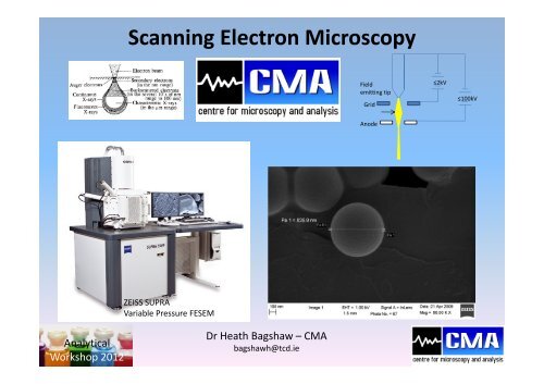
<strong>Scanning</strong> <strong>Electron</strong> <strong>Microscopy</strong><br />
Field<br />
emitting tip<br />
Grid<br />
≤2kV<br />
≤100kV<br />
Anode<br />
ZEISS SUPRA<br />
Variable Pressure FESEM<br />
Analytical<br />
Workshop 2012<br />
Dr Heath Bagshaw – CMA<br />
bagshawh@tcd.ie
Why use an SEM?<br />
Analytical<br />
Workshop 2012<br />
Fig 1. Examples of features resolvable using different imaging techniques
Improving Resolution<br />
• Firstly, the wavelength of the imaging source is important.<br />
In an optical microscope white light is used (λ – 380-700-nm)<br />
• In an <strong>Electron</strong> Microscope the imaging source is a beam of electrons which has a<br />
shorter wavelength (λ ~0.0025nm at 200kV) .<br />
• This is approximately five times smaller than visible light and twice as small as a<br />
typical atom – this is why electrons can ‘see’ atoms but white light can’t :-<br />
Analytical<br />
Workshop 2012<br />
‘the analysis probe must be smaller than the feature being analysed’<br />
• The wavelength of electrons is dependent on the accelerating voltage, i.e.:-<br />
kV<br />
Wavelength λ (pm)<br />
20 8.588<br />
100 3.702<br />
200 2.508<br />
300 1.968<br />
• The higher the accelerating voltage the shorter the wavelength.
The Parts of an EM<br />
• <strong>Electron</strong> Microscopes (EMs) are similar in operation to optical microscopes except<br />
that they use a focused beam of electrons instead of light to "image" the specimen and<br />
gain information about its structure and composition.<br />
• There are four major regions in an <strong>Electron</strong> Microscope:-<br />
Analytical<br />
Workshop 2012<br />
(1) A stream of electrons is formed (by the electron source/gun) and<br />
accelerated toward the specimen using a positive electrical potential<br />
(2) This stream is confined and focused using metal apertures and magnetic<br />
lenses into a thin, focused, monochromatic beam.<br />
(3) This beam is focused onto the sample using a magnetic lens. In an SEM<br />
the beam is then also scanned across the surface of the sample.<br />
(4) Interactions occur inside the irradiated sample, affecting the electron<br />
beam which are detected and transformed into an image or signal.<br />
• The above happens in all EMs regardless of type.
Layout of a Generic SEM<br />
Gun<br />
1<br />
Aperture<br />
Holder<br />
2<br />
Deflection<br />
coils<br />
3<br />
Objective Lens<br />
4<br />
Analytical<br />
Workshop 2012
<strong>Electron</strong> Gun<br />
• There are two main types of gun – Thermionic and Field Emission (FEG).<br />
• Thermionic gun :- Simplistically, a material (often a piece of twisted tungsten) is heated<br />
to a high temperature so that it will emit electrons.<br />
• Can also use LaB 6 crystal grown to a tip – gives a brighter beam than W for same kV.<br />
Analytical<br />
Workshop 2012<br />
Tungsten filament Tungsten filament assembly LaB 6 filament tip
Thermionic Gun<br />
Filament<br />
Wehnelt<br />
cylinder<br />
-<br />
10-10000kV<br />
+<br />
Anode<br />
earth<br />
•Filament is heated and begins to produce electrons.<br />
•<strong>Electron</strong>s leave the filament tip with a negative potential so accelerate towards the<br />
earthed anode and into the microscope column.<br />
•A small negative bias on the Wehnelt then focuses the beam to a crossover which acts as<br />
the electron source.<br />
Analytical<br />
Workshop 2012
Field Emission Gun (FEG)<br />
FEG source – W tip<br />
• A very strong magnetic field (~10 9 Vm -1 ) draws electrons from a very fine metallic tip<br />
(usually W).<br />
•An extraction voltage of around 2kV is applied to the first anode to create an intense<br />
electric field to allow electrons to escape from the tip.<br />
•The second anode is then used to accelerate the electrons into the microscope at the<br />
required energy.<br />
•Combination of the two anodes focuses the beam into a crossover creating a fine<br />
beam source.
Comparison of Sources<br />
•W filaments are very simple and inexpensive.<br />
•LaB 6 filaments give greater brightness than W (approximately X10), but cost more.<br />
•FEG’s give much more brightness than thermionic systems.<br />
•FEG’s give a more monochromatic electron source and finer probe (i.e. better resolution).<br />
•Temperatures used are much lower than for thermionic sources (particularly cold cathode<br />
FEG’s).<br />
•FEG’s require better vacuum systems and are more expensive.<br />
Analytical<br />
Workshop 2012<br />
Comparison of the three types of source<br />
operating at 100kV
Focusing the Beam<br />
• After the beam is formed it is focused by a condenser lens system to form a ‘probe’.<br />
• The lenses are electromagnetic – the focal length changes as current in the coil changes.<br />
• After focusing, the beam is passed through an aperture which excludes electrons which are<br />
not on the optical axis – improving resolution.<br />
• Inconsistencies in the beam are corrected by stigmators and the beam focused onto the<br />
sample.<br />
A typical Electro<br />
Magnetic Lens<br />
Analytical<br />
Workshop 2012
<strong>Scanning</strong> the Beam\Beam Interactions<br />
• Deflector coils move the beam back and forth over the sample and the signal<br />
generated from each area is collected simultaneously, building up the final image<br />
shown on the monitor.<br />
• Many signals are generated at the surface of the<br />
sample and many different forms of analysis may be<br />
performed.<br />
• The ‘interaction volume’ is the area of the sample<br />
excited by the electron beam to produce a signal.<br />
Incident <strong>Electron</strong>s<br />
(<strong>Electron</strong> Probe)<br />
Auger <strong>Electron</strong>s<br />
Secondary <strong>Electron</strong>s<br />
Backscattered <strong>Electron</strong>s<br />
Continuum X-Rays<br />
Fluorescence X-Rays<br />
Characteristic X-Rays<br />
Signals generated in the interaction volume<br />
Analytical<br />
Workshop 2012
Interaction Volume<br />
•The ‘interaction volume’ is the area of the sample excited by the electron beam to<br />
produce a signal.<br />
•The penetration of the electron beam into the sample is affected by the accelerating<br />
voltage used, the higher the kV the greater the penetration.<br />
•The effective interaction volume can be calculated using the electron range, R:-<br />
1.67<br />
0.0276<br />
A E0<br />
R =<br />
( µ m)<br />
0.89<br />
ρ Z<br />
Where A is the atomic weight (g/mole), Z is the atomic number, ρ is the density (in g/cm 3 ) and E o is the energy of<br />
the primary electron beam (in kV).<br />
Take the example of iron:<br />
A=55.85, Z=26, r=7.87 g/cm 3<br />
Accelerating voltage (kV) Primary <strong>Electron</strong> Range (µm)<br />
30 3.1<br />
15 0.99<br />
5 0.16<br />
1 0.01 (10nm!)<br />
Signals generated in the interaction volume<br />
Analytical<br />
Workshop 2012
Signal Detection<br />
• The Everhard – Thornley Detector (ETD) is the most common detector used to detect<br />
secondary electrons to image surface topography.<br />
• <strong>Electron</strong>s are attracted to a +ve charge on a grid in front of the detector. The captured<br />
electrons are then amplified by a photo-multiplier before being digitised and sent to a screen.<br />
• The signal detected is transferred to a viewing screen as the beam is scanned building up the<br />
image.<br />
Everhard Thornley Detector<br />
<strong>Scanning</strong> to produce an image<br />
Analytical<br />
Workshop 2012
Biological Samples<br />
•Biological samples are not conductive and are particularly vulnerable to beam damage and<br />
other heating effects when examined in an <strong>Electron</strong> Microscope.<br />
•The level of exposure is referred to as ‘<strong>Electron</strong> Dose’ and is a measure of the number of<br />
electrons per unit area (e/nm 2 ).<br />
•Samples are either stained with conductive materials (e.g. OsO 4 ) or coated with Au or C.<br />
•Samples are viewed under vacuum, so they are dried to remove all water.<br />
a) b)<br />
•a) SEM image of Pneumonia, and b) SEM image of Diatom (Pictures from University of Iowa)<br />
•Preparing the samples ‘fixes’, and alters them – need a way to look at samples whilst they are<br />
still ‘wet’.<br />
Analytical<br />
Workshop 2012
Variable Pressure SEM<br />
•Localised charging is removed by the presence of gas in the sample chamber, effectively allowing the<br />
examination of non conductive samples<br />
•In Low vacuum mode the chamber is isolated from the high vacuum system(A) and is instead pumped<br />
by the additional rotary pump system(B).<br />
Analytical<br />
Workshop 2012
Variable Pressure SEM (2)<br />
• This allows analysis of ‘non conducting’ samples as charge is compensated by gas in the<br />
chamber.<br />
• Use of an SEM in VP mode does lead to some limitations in it’s operation:-<br />
• Because the vacuum is lower in a VPSEM chamber, some resolution of the instrument is<br />
lost due to scattering of the electron beam by the gas particles in the chamber.<br />
• In situ heating and or cooling (with the appropriate sample stage) is possible in VPSEM<br />
to allow direct observation of sample changes.<br />
• Compositional analysis is still possible.<br />
Analytical<br />
Workshop 2012
Compositional Analysis – Back Scattered Imaging<br />
• As mentioned previously, when the electron beam hits the sample a number of signals<br />
are generated. Secondary electrons are used for looking at surface detail (topography).<br />
• EM is also a very powerful technique for analysing composition and compositional<br />
distribution in a material\sample.<br />
B<br />
Analytical<br />
Workshop 2012<br />
Signals generated in the interaction volume<br />
• Back Scattered electrons are produced just below the surface of the sample (B) and are<br />
scattered more by heavier elements than by lighter elements.<br />
• The backscattered coefficient, η = (Z-1.5)/6 So, as Z increases, so does the degree of<br />
backscatter.
Back Scattered <strong>Electron</strong>s<br />
0.5 Backscattered<br />
electrons<br />
0.4<br />
<strong>Electron</strong> yield<br />
0.3<br />
0.2<br />
0.1<br />
Secondary electrons<br />
0 20 40 60 80<br />
Atomic number (Z)<br />
<strong>Electron</strong> yield (i.e. intensity) as a function of atomic number for backscattered and Secondary<br />
electrons.<br />
• Back Scattered electron have approximately the same energy as the primary electron<br />
beam and are therefore easy to detect - simply by a semiconductor placed above the<br />
sample :-<br />
Analytical<br />
Workshop 2012<br />
Schematic of a backscattered electron detector.
BackScattered Imaging<br />
• Back scattered electrons are deflected more by heavier atoms leading to a brighter<br />
contrast in BEI images – the lighter the region the heavier the element present.<br />
a)<br />
b)<br />
White<br />
region<br />
Dark<br />
region<br />
Grey<br />
region<br />
• a)Secondary image of a cement showing surface morphology<br />
• b)Backscattered image of same area showing compositional inhomogeneity<br />
• Three distinct regions in b), EDS analysis can then be used to find the different<br />
compositions of the these regions.<br />
Analytical<br />
Workshop 2012
Example EDS of a Cement<br />
• There were 3 distinct regions in the Backscattered Image<br />
‘Light’ region is made up predominantly of<br />
Fe. (i.e. the heaviest element)<br />
‘Grey’ region is made up predominantly of<br />
Ca.<br />
‘Dark’ region is made up predominantly of Si<br />
and Al. (i.e. the lightest elements)<br />
Analytical<br />
Workshop 2012
Examples Images<br />
Imaged using ET Detector<br />
Imaged using InLens Detector<br />
Analytical<br />
Workshop 2012<br />
Low kV image of platelets
Examples Images<br />
SE image of nano tubes<br />
BE image of nano tubes<br />
Analytical<br />
Workshop 2012<br />
SE Image of nano structure
Conclusions<br />
•<strong>Scanning</strong> <strong>Electron</strong> Microscopes (SEM’s) are very useful tools for looking at a range of<br />
samples\materials.<br />
•Surface detail, homogeneity and elemental composition can be determined in one<br />
experiment on the same sample.<br />
•Newer Variable Pressure SEM’s allow the imaging of non conducting samples.<br />
•ESEM’s, with cold stages and other peripherals allow imaging at 100% relative humidity<br />
allowing imaging of ‘wet’ samples<br />
•<strong>Electron</strong> <strong>Microscopy</strong> based analysis when used with other analysis techniques can<br />
assist in complete characterisation\identification of materials.<br />
•<strong>Electron</strong> Microscopes provide a very powerful analysis tool in both Materials and<br />
biological fields.<br />
Analytical<br />
Workshop 2012