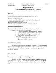
Experiment 8 Introduction to VHDL
Experiment 8 Introduction to VHDL
Experiment 8 Introduction to VHDL

You also want an ePaper? Increase the reach of your titles
YUMPU automatically turns print PDFs into web optimized ePapers that Google loves.
ELCTEC-131 Advanced Digital Electronics MATC<br />
Richard Lokken<br />
Adapted for the DE1 board<br />
<strong>Experiment</strong> 8<br />
<strong>Introduction</strong> <strong>to</strong> <strong>VHDL</strong><br />
Objectives:<br />
Upon completion of this labora<strong>to</strong>ry exercise, you should be able <strong>to</strong>:<br />
• Enter a simple combinational logic circuit in <strong>VHDL</strong> using the Quartus II Text<br />
Edi<strong>to</strong>r.<br />
• Assign a target device and pin numbers and compile a <strong>VHDL</strong> design file.<br />
• Write simulation criteria for a <strong>VHDL</strong> design entity and create a simulation <strong>to</strong><br />
verify the correctness of the design.<br />
• Download the file <strong>to</strong> an Altera CPLD on the Aletera DE1 board.<br />
Lab<br />
Reference and Equipment Required:<br />
• Dueck, Robert K., Digital Design with CPLD Applications and <strong>VHDL</strong>, 2/e<br />
• Chapter 5: <strong>Introduction</strong> <strong>to</strong> <strong>VHDL</strong><br />
• CPLD Trainer: Altera DE1 board development kit<br />
• Quartus II Web Edition Software<br />
<strong>Experiment</strong>al Notes<br />
<strong>VHDL</strong> stands for VHSIC Hardware Description Language (VHSIC = Very High<br />
Speed Integrated Circuit). <strong>VHDL</strong> is an industry-standard programming language for<br />
simulation and synthesis of digital circuits. In this lab, we will use <strong>VHDL</strong> <strong>to</strong> enter the<br />
designs for some simple combinational logic circuits, using <strong>VHDL</strong> constructs for<br />
Boolean equations and truth tables.<br />
Every <strong>VHDL</strong> design requires an entity declaration, which describes the inputs<br />
and outputs of the design, and an architecture body, which describes the internal<br />
relationship between inputs and outputs. Within the architecture body, we can use many<br />
different language statements <strong>to</strong> describe our design. We will use two of the simplest: a<br />
concurrent signal assignment statement, which can be used <strong>to</strong> implement a Boolean<br />
expression, and a selected signal assignment statement, which can be used, among<br />
other things, <strong>to</strong> implement a truth table.<br />
Figure 8.1 shows the majority vote circuit constructed in Lab 7. The circuit has<br />
the Boolean expression Y = AB + AC + BC. The output is HIGH if at least two out of
ELCTEC-131 Advanced Digital Electronics MATC<br />
Richard Lokken<br />
Adapted for the DE1 board<br />
three inputs are HIGH. A concurrent signal assignment statement would encode this<br />
equation as follows:<br />
y
ELCTEC-131 Advanced Digital Electronics MATC<br />
Richard Lokken<br />
Adapted for the DE1 board<br />
D2 D1 D0 Y<br />
0 0 0 0<br />
0 0 1 1<br />
0 1 0 1<br />
0 1 1 0<br />
1 0 0 1<br />
1 1 0 0<br />
1 1 1 0<br />
Table 8.1 Sample Truth Table<br />
In the entity declaration of a <strong>VHDL</strong> file, we can define the combined input values<br />
of D2,D1, and D0 as a 3-bit vec<strong>to</strong>r of type STD_LOGIC_VECTOR:<br />
d: IN STD_LOGIC_VECTOR(2 down<strong>to</strong> 0);<br />
This truth table can be encoded by the following selected signal assignment statement:<br />
WITH d SELECT<br />
y
ELCTEC-131 Advanced Digital Electronics MATC<br />
Richard Lokken<br />
Adapted for the DE1 board<br />
BEGIN<br />
WITH d SELECT<br />
y
ELCTEC-131 Advanced Digital Electronics MATC<br />
Richard Lokken<br />
Adapted for the DE1 board<br />
Figure 8.2 Majority Vote Simulation<br />
Procedure<br />
Encoding a Circuit with a Concurrent Signal Assignment Statement<br />
Refer <strong>to</strong> the half-adder circuit shown in Figure 8.3.<br />
A<br />
INPUT<br />
VCC<br />
XOR<br />
OUTPUT<br />
sum<br />
inst<br />
AND2<br />
B<br />
INPUT<br />
VCC<br />
inst1<br />
OUTPUT<br />
carry _out<br />
Figure 8.3 Half-Adder Circuit<br />
Design Entry<br />
• Create a new folder called drive:\qdesigns\labs\lab08\half_add\.<br />
• Use the Quartus II Text Edi<strong>to</strong>r <strong>to</strong> enter the <strong>VHDL</strong> file for the half-adder circuit,<br />
using a concurrent signal assignment statement, as described in the <strong>Experiment</strong>al<br />
Notes for this lab exercise.
ELCTEC-131 Advanced Digital Electronics MATC<br />
Richard Lokken<br />
Adapted for the DE1 board<br />
• Save the file as drive:\qdesigns\labs\lab08\half_add\half_add.vhd and use the<br />
file <strong>to</strong> create a project in Quartus II. (Make sure that the box labeled Create new<br />
project based on this file is checked.)<br />
• In the New Project Wizard, assign the target device as EP2C20F484C7.<br />
• From the Assignments menu, select Assign pins. Assign the pin numbers in<br />
Table 8.2 <strong>to</strong> the circuit inputs and outputs, choosing the column that pertains <strong>to</strong><br />
your DE1 board.<br />
• When you have finished assigning the pin numbers, compile the project.<br />
Simulation<br />
Pin Name DE1 Board Description<br />
A PIN_L2 Toggle Switch[9]<br />
B PIN_M1 Toggle Switch[8]<br />
Sum PIN_R17 LED Red[9]<br />
Carry_out PIN_R18 LED Red[8]<br />
Table 8.2 Pin Assignments for Half-Adder<br />
• Write a set of simulation criteria for the half-adder function.<br />
Simulation Criteria:<br />
• Use the simulation criteria <strong>to</strong> create a Quartus II simulation for the half-adder.<br />
Programming the CPLD Board<br />
• Download the project <strong>to</strong> your CPLD trainer board.<br />
• Connect two DIP switches <strong>to</strong> inputs a and b and two LED indica<strong>to</strong>rs <strong>to</strong> outputs<br />
carry_out and sum.<br />
• Close the project for the half adder by selecting Close Project from the File<br />
menu.<br />
•<br />
Encoding a Circuit with a Selected Signal Assignment Statement<br />
• Examine the SOP logic gate network shown in Figure 8.4. Inputs are labeled d3,<br />
d2, d1, d0.
ELCTEC-131 Advanced Digital Electronics MATC<br />
Richard Lokken<br />
Adapted for the DE1 board<br />
• Write the Boolean expression of the logic gate network shown in Figure 8.3.<br />
• Note that the Boolean expression is already in its simplest SOP form. Because this<br />
equation would be difficult <strong>to</strong> read (and code) in <strong>VHDL</strong>, we will use a selected<br />
signal assignment statement <strong>to</strong> encode the circuit’s truth table.<br />
Design Entry<br />
• Create a new folder called drive:\qdesigns\labs\lab08\sop1\.<br />
• Write a <strong>VHDL</strong> file for the logic gate network in Figure 8.4, using a selected<br />
signal assignment statement <strong>to</strong> encode its truth table. Write the d inputs as a<br />
single variable of type STD_LOGIC_VECTOR.<br />
• Save the file as drive:\qdesigns\labs\lab08\sop1\sop1.vhd and use this file <strong>to</strong><br />
create a new project in Quartus II.<br />
• In the New Project Wizard, assign the target device as EP2C20F484C7.<br />
• Assign pin numbers <strong>to</strong> the <strong>VHDL</strong> file as shown in Table 8.4.<br />
Pin Name Pin Number Description<br />
d3 PIN_L2 Toggle Switch[9]<br />
d2 PIN_M1 Toggle Switch[8]<br />
d1 PIN_M2 Toggle Switch[7]<br />
d0 PIN_U11 Toggle Switch[6]<br />
y PIN_R17 LED Red[9]<br />
Table 8.4 Pin Assignments for Figure 8.4
ELCTEC-131 Advanced Digital Electronics MATC<br />
Richard Lokken<br />
Adapted for the DE1 board<br />
Simulation<br />
Figure 8.4 Sum-of-Products Logic Gate Network<br />
• Write a set of simulation criteria for the SOP function in your <strong>VHDL</strong> file.<br />
Simulation Criteria:<br />
• Use the simulation criteria <strong>to</strong> create a Quartus II simulation for the <strong>VHDL</strong> design<br />
entity.<br />
Programming the CPLD Board<br />
• Download the project <strong>to</strong> your DE1 board.
ELCTEC-131 Advanced Digital Electronics MATC<br />
Richard Lokken<br />
Adapted for the DE1 board<br />
• Write the truth table for the circuit in Figure 8.4.<br />
• Close the project for the SOP circuit by selecting Close Project from the File<br />
menu.