User Manual for Daughter Card
User Manual for Daughter Card
User Manual for Daughter Card

Create successful ePaper yourself
Turn your PDF publications into a flip-book with our unique Google optimized e-Paper software.
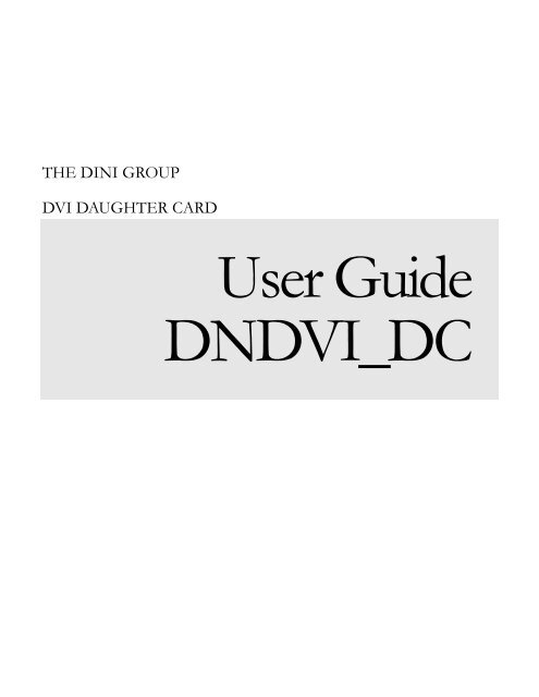
THE DINI GROUP<br />
DVI DAUGHTER CARD<br />
<strong>User</strong> Guide<br />
DNDVI_DC
L O G I C E M U L A T I O N S O U R C E<br />
DNDVI_DC <strong>User</strong> <strong>Manual</strong> Version 1.1<br />
© The Dini Group<br />
1010 Pearl Street • Suite 6<br />
La Jolla, CA92037<br />
Phone 858.454.3419 • Fax 858.454.1279<br />
support@dinigroup.com<br />
www.dinigroup.com<br />
Last Modified: 8/3/2007 11:12:51<br />
Last saved by jthurkettle
Chapter<br />
0<br />
DNDVI_DC<br />
<strong>Daughter</strong> <strong>Card</strong><br />
Chapter1:Welcome to<br />
Congratulations on your purchase of the DNDVI_DC<br />
<strong>Daughter</strong> <strong>Card</strong>!
Q U I C K S T A R T G U I D E<br />
Chapter<br />
1<br />
1 Quick Start Guide<br />
The Dini Group DNDVI_DC is the user-friendliest board available with a Virtex<br />
4 FPGA and two DVI interface<br />
1.1 What’s provided<br />
First, let’s examine the contents of your DNDVI_DC kit. It should contain:<br />
• DNDVI_DC board<br />
• RS 232 IDC header cable to female DB9<br />
• CD ROM containing:<br />
o Virtex 4 Reference Design<br />
o <strong>User</strong> manual PDF<br />
o Board Schematic PDF<br />
o DNDVI_DC firmware<br />
DNDVI_DC <strong>User</strong> Guide www.dinigroup.com 3
D N D V I _ D C<br />
The Dini Group can optionally provide the following accessories:<br />
• Memory modules <strong>for</strong> use in the DNDVI_DC DDR2 SODIMM socket<br />
- QDRII SRAM 64x1Mb, 300Mhz<br />
- Flash memory 32x4Mb, 2x4Mb serial flash<br />
- Reduced Latency DRAM (RLDRAM) 64x8Mb, 300Mhz<br />
- Standard SRAM, 64x2M (Select ZBT/sync-burst, Pipelined/Flow through)<br />
- Test connection module (with two Mictor38)<br />
You may also want to obtain from a third party vendor:<br />
• Xilinx Parallel Cable IV or Xilinx Plat<strong>for</strong>m Cable USB<br />
• 200-pin DDR2 SODIMM<br />
• Synplicity Identify, or Xilinx Chipscope <strong>for</strong> embedded logic analyzer functionality.<br />
• LCD monitor with DVI input [Any DVI 1.0 compliant monitor should suffice].<br />
• Video card with DVI output.<br />
• Video camera with DVI output.<br />
1.2 Precaution<br />
The DNDVI_DC is sensitive to static electricity, so treat the PCB accordingly. The target markets <strong>for</strong> this<br />
product are engineers that are familiar with FPGAs and circuit boards. However, if needed, the following web<br />
page has an excellent tutorial on the “Fundamentals of ESD” <strong>for</strong> those of you who are new to ESD sensitive<br />
products:<br />
http://www.esda.org/basics/part1.cfm<br />
There are four ground test points on the DNDVI_DC.<br />
The DNDVI_DC has been factory tested and pre-programmed to ensure correct operation. You do not need<br />
to alter any jumpers or program anything to see the board work. A reference design is included on the provided<br />
CD.<br />
The 200-pin connector is not 5V tolerant. According to the Virtex 4 datasheets, the maximum applied voltage<br />
to these signals is VCCO + 0.5V (3.0V while powered on). These connections are not buffered, and the Virtex<br />
4 part is sensitive to ESD. Take care when handling the board to avoid touching the daughter card connectors.<br />
DNDVI_DC <strong>User</strong> Guide www.dinigroup.com 4
D N D V I _ D C<br />
1.3 Power-On Instructions<br />
The image below represents your DNDVI_DC. You will need to know the location of the following parts<br />
referenced in this chapter.<br />
To begin working with the DNDVI_DC, follow the steps below :<br />
1.4 Verify Switch Settings<br />
The DNDVI_DC uses a DIP switch to program the FPGA configuration circuitry. The function of these DIP<br />
switches is listed in Table 2. Verify that the switch settings on your board match the default settings.<br />
DNDVI_DC <strong>User</strong> Guide www.dinigroup.com 5
D N D V I _ D C<br />
Table 1 - Switch Description<br />
Switch<br />
Default<br />
Position<br />
S1-1 Off CFG_REV0<br />
S1-2 Off CFG_REV1<br />
S1-3 Off CFG_REVSEL<br />
Signal Name On setting Off setting<br />
When CFG_REVSEL is ON - CFG_REV0<br />
and CFG_REV1 are used to select the design<br />
revision to be enabled, overriding the internal<br />
programmable revision selection control bits.<br />
S1-4 Off DIPSW4 Configurable Configurable<br />
1.5 Memory and heat sinks<br />
There should be an active heat sink installed on the FPGA on the DNDVI_DC. Virtex 4 FPGAs are capable<br />
of dissipating 15W or more, so you should always run the board with the heat sink installed.<br />
The DNDVI_DC comes packaged without memory installed. If you want the Dini Group reference design to<br />
test your memory module, you can install it now in the 1.8V DDR2 DIMM socket.<br />
DNDVI_DC <strong>User</strong> Guide www.dinigroup.com 6
D N D V I _ D C<br />
The socket DDR2_SODIMM can accept any capacity DDR2 SODIMM. Note that DDR1 modules will not<br />
work in these slots since they are supplied with 1.8V power and DDR1 requires 2.5V power (and a completely<br />
different pin-out). [Note that the Dini Group has a DDR2 module that provides a DDR1 socket, even so,<br />
changing all the voltages would still be required.]<br />
1.6 Power Up Procedure<br />
1. Plug the four pin hard drive power connector from the power supply into P2. Make sure your work<br />
area is clear and there are no metal wrenches under the board. Turn on the power supply.<br />
When the DNDVI_DC powers on, it automatically loads Xilinx FPGA design bit file stored in the PROM (if<br />
the load FPGA option was selected during PROM programming).<br />
To load a different Xilinx bit program file into the DNDVI_DC follow the steps outlined in section 2.4.<br />
1.7 Loading FPGA configuration once<br />
The DNDVI_DC reads FPGA configuration data from the JTAG chain. To program the FPGA on the<br />
DNDVI_DC, FPGA design file (with a .bit file extension) are uploaded through the JTAG chain. This can be<br />
accomplished using the Xilinx ISE iMPACT tool.<br />
Step by step instructions <strong>for</strong> loading bit file into the FPGA via iMPACT.<br />
1. Attach the Xilinx JTAG cable to J8 on the DNDVI_DC<br />
2. Start iMPACT.<br />
DNDVI_DC <strong>User</strong> Guide www.dinigroup.com 7
D N D V I _ D C<br />
3. Create a new project in iMPACT [file -> new -> create new project]<br />
4. Choose “Configure devices using Boundary-Scan (JTAG)” as the project action.<br />
5. Bypass the first “Assign New Configuration File” pop-up menu.<br />
6. Select the FPGA design bit file in the second “Assign New Configuration File” pop-up menu.<br />
7. Right click on the FPGA in the JTAG chain display select program and then OK at the<br />
“Programming Properties” menu.<br />
1.8 Loading FPGA bitfile into the PROM<br />
There is an XCF32P Xilinx FLASH-PROM on the board to allow the FPGA to automatically be programmed<br />
when the board is powered on. To use this feature, the ISE tools must be version 7.1sp3 or newer.<br />
1. Attach a Xilinx JTAG cable to J8 on the DNDVI_DC.<br />
2. Start iMPACT.<br />
3. Create a new project in iMPACT.<br />
4. Choose “Prepare a PROM File” as the project action.<br />
5. Target: “Xilinx PROM”, “MCS” file <strong>for</strong>mat, and give it a filename.<br />
6. Select an “xcf32p” as the PROM Device, and add it to the list.<br />
7. When it brings up the GUI, and asks <strong>for</strong> a “.bit” file, give it your “.bit” file generated by the<br />
ISE tools. Don’t add a second “.bit” file, because there is only 1 FPGA on the board.<br />
8. Now generate the “.mcs” output file by double clicking on “Generate File”. Go check to make<br />
sure that the “.mcs” file was created.<br />
9. To program that “.mcs” file into the Prom:<br />
a. Switch iMPACT to boundary scan mode.<br />
b. Initialize the JTAG chain. It should find the “xcf32p” and the “xc4vfx60/100” devices.<br />
c. Assign the “.mcs” file as the programming file <strong>for</strong> the “xcf32p”.<br />
d. “Bypass” the programming file <strong>for</strong> the “xc4vfx60/100”.<br />
e. Double click “Program” while the “xcf32p” is selected. Make sure to select “Verify”,<br />
“Erase Be<strong>for</strong>e Programming”, and “Load FPGA” from the options given in the<br />
programming window. Hit “OK” and wait <strong>for</strong> about 2 minutes until the programming has<br />
completed.<br />
DNDVI_DC <strong>User</strong> Guide www.dinigroup.com 8
D N D V I _ D C<br />
10. Now when the board is power-cycled, it will automatically have the “.mcs” file loaded into the<br />
FPGA.<br />
1.9 Check LED status lights<br />
The DNDVI_DC has many status LEDs to help the user confirm the status of the configuration process.<br />
1. Check the power voltage indication LEDs to confirm that all voltage rails of the DNDVI_DC<br />
are present. The LEDs indicate the presence of 12V, 5V, 3.3V, 2.5V, and 1.8V<br />
2. Check the Configuration status LED. When the FPGA has been successfully configured the<br />
FPGA_DONE LED will illuminate.<br />
You should also verify the fan mounted above the Virtex 4 FPGA is spinning.<br />
1.10 Finished Quick Start<br />
At this point either a reference design is loaded or a user supplied design is loaded in the DN_DVI<br />
board. If you wish to verify the reference design move on to chapter 2.<br />
DNDVI_DC <strong>User</strong> Guide www.dinigroup.com 9
D N D V I _ D C<br />
Chapter<br />
2<br />
2 Testing the Reference design using the<br />
Included software<br />
To test the reference design on the daughter card, the DNDVI_DC provides tests <strong>for</strong><br />
the following options out of the box.<br />
• DVI RX0, RX1, TX0, TX1<br />
• 200-pin SODIMM socket<br />
• RS232 Loopback<br />
• Rocket IO<br />
The 4 DVI connectors allow single-link and dual-link digital video to be received and<br />
transmitted.<br />
The RS232 interface allows low-speed data transfers to and from the <strong>User</strong> design.<br />
A DDR2 SDRAM SODIMM can be installed in the 200-pin SODIMM socket, or one<br />
of our other cards (SSRAM, FLASH, Mictor, …) can be installed instead.<br />
The 200-pin header can be used to connect the DNDVI_DC to many of the<br />
DiniGroup FPGA emulation boards (check http://www.dinigroup.com <strong>for</strong> the<br />
compatibility list).<br />
This section will get you started and show you how to operate the provided software.<br />
2.1 DVI reference design<br />
The FPGA is initially programmed with a reference design that will receive DVI video<br />
on RX0, and send it back out on TX0. (The RST switch may need to be applied after<br />
changing input frequencies). The same is true <strong>for</strong> RX1 and TX1.<br />
DNDVI_DC <strong>User</strong> Guide www.dinigroup.com 10
There is also sample code that can be un-commented in the reference design<br />
that will generate a simple video output pattern (without requiring a DVI input cable<br />
connected to RX0).<br />
11
NOTE: If you are using a dual link signaling you MUST use dual link DVI<br />
cables. Dual link DVI cables can be identified by the pin out on the connector.<br />
2.2 Communicating to the <strong>User</strong> Design over the Serial Port<br />
You may want to communicate with your design over the user serial port (P3).<br />
Connect a RS232 cable to P3, the FPGA RS232.<br />
The reference design is programmed to digitally loop back the input to the output. No<br />
hardware flow control is supported. If on the terminal you see a local echo, then the<br />
12
eference design was able to capture the RS232 signal and generate an RS232 signal<br />
that your computer could capture.<br />
2.3 DDR2 SODIMM TEST<br />
The provided test design automatically runs a DDR2 memory test with status indicated<br />
by the LEDs. After reset LED 5 will go high <strong>for</strong> approximately 20 seconds followed<br />
by LED indicators of the memory test. LED10-9 indicate test stage. 00 indicates initial<br />
stage, 01 indicates write read test, 10 indicates read back test, 11 indicates successful<br />
completion of tests. If an error occurs the LEDS will indicate which test failed and<br />
indicate the LSB of error in the memory.<br />
13
2.4 RocketIO TEST<br />
On the CD accompanying the DNDVI board in the bit file directory one can find the<br />
RocketIO MCS file. Load the MCS file into the PROM following the steps outlined in<br />
section 2.5. Connect SMA cables in loop back configuration on all eight of the<br />
RocketIO pairs. [That is to say connect TXP to RXP and TXN to RXN]. Reset or<br />
power on the board after all the connections have been made. If test passes all 10<br />
LEDS should flash on and off. The image above shows the loopback configuration<br />
<strong>for</strong> pair 3.<br />
The following is an explicit list of pair matching.<br />
[J12-J13], [J23-J14], [J24-J34], [J25-J35], [J36-J38], [J37-J39], [J26-J15], [J27-J16], [J28-<br />
J40], [J29-J41], [J17-J42], [J18-J43], [J30-J19], [J31-J20], [J32-J21], [J33-J22]<br />
14
Chapter<br />
3<br />
3 DNDVI_DC Hardware<br />
3.1 ERRATA<br />
Please note – On the Revision 1.0 boards a jumper wire has been added to<br />
the bottom of the board between R244 and the non-power side of R325. This<br />
is not reflected in the schematic.<br />
3.2 Multiplexed Serial Port<br />
The DNDVI_DC has one serial port (P3) <strong>for</strong> user use. No configuration is required to<br />
enable the first serial port. This can be extended to two serial ports by use of a<br />
breakout serial cable. LED5 and LED6 are tied to the second serial ports TX and RX<br />
respectively.<br />
Serial port 1 uses pins 2 and 3. Serial port 2 uses pins 6 and 7 of port P3.<br />
To enable the second RS232 Port: Add the following 0 Ohm resistors. R350, R352,<br />
R362, R360. This will enable the second serial port on pins 6 and 7 on P3. For more<br />
details see page 07 in the Schematic. “P07: MISC. PERIPHERALS”.<br />
15
Chapter<br />
4<br />
4 Clocking Overview<br />
This chapter discusses the various clocks available on the DNDVI_DC and any user<br />
settable options available.<br />
16
4.1 Block Diagram of the DNDVI_DC clocks:<br />
17
4.2 List of Input Clocks<br />
When shipped the DNDVI board has several clock sources available.<br />
DIFFERENTIAL:<br />
• 200 Mhz Oscillator [U34] : H17/J17<br />
• 250 Mhz Oscillator [U45] : M34/N34 [<strong>for</strong> MGT use only]<br />
• 250 Mhz Oscillator [U28] : J1/K1 [<strong>for</strong> MGT use only]<br />
• ICS8442 Clock Generator [U31]: J16/J15<br />
• ICS8442 Clock Generator [U32]: J14/K14<br />
• ICS843020 Clock Generator [U44]: [AP29/AP28], [AP3/AP4] : [<strong>for</strong> MGT<br />
use only]<br />
• Note: Pins 2/3 on H5 can be configured as an input clock at the expense<br />
of two LEDs - See Schematic page P09_CLOCKS <strong>for</strong> details: H19/H18.<br />
• Note: Pins 2/3 on H8 can be configured as an input clock at the expense<br />
of two LEDs - See Schematic page P09_CLOCKS <strong>for</strong> details:<br />
AF18/AG18.<br />
DIFFERENTIAL FEEDBACK CLOCKS:<br />
• TX0 PLL CDCU877 [U33]: K18/K17<br />
• TX1 PLL CDCU877 [U27]: K19/J19<br />
• DDR PLL CDCU877 [U53]: L15/L14<br />
SINGLE ENDED CLOCKS:<br />
• RX0 [U9]: AD21<br />
• RX1 [U12]: AE18<br />
• EXPCON_CCLK [P4] : AF16<br />
• EXPCON_DCLK [P4] : AG17<br />
• EXPCON_ECLK [P4]: AE21<br />
18
4.3 List of Output Clocks<br />
SINGLE ENDED CLOCKS:<br />
• EXPCON_CLKIN [P4]: AF20<br />
• GP_I2C_SCL : AE17 : Note that this is the general I2C clock <strong>for</strong> the<br />
board and attaches to both the FPGA temperature sensor and the DDR2<br />
connector.<br />
• RX0_CLK_FWD [U31]: U7 - Note: By default this clock is ignored on<br />
the ICS8442, see schematic <strong>for</strong> details.<br />
• RX1_CLK_FWD [U32]: U6 - Note: By default this clock is ignored on<br />
the ICS8442, see schematic <strong>for</strong> details.<br />
• RX0_I2C_SCL [U21]: AH9<br />
• RX1_I2C_SCL [U22]: V3<br />
• TX0_I2C_SCL [U6/U3]: AF13 – Note: This attaches to both the SIL178<br />
and J2 output.<br />
• TX1_I2C_SCL [U4/U8]: AM10 -- Note: This attaches to both the SIL178<br />
and J3 output.<br />
• TX0_CLKGEN_SCLK [U31]: L31<br />
• TX1_CLKGEN_SCLK [U32]: L30<br />
• MGTCG1_SCLK [U44]: J32<br />
• TX0_M_BYPASS_CLK : AB5 – Note: Ignored by default, see schematic<br />
<strong>for</strong> details.<br />
• TX0_S_BYPASS_CLK : AD5 – Note: Ignored by default, see schematic<br />
<strong>for</strong> details.<br />
• TX1_M_BYPASS_CLK : AG8 – Note: Ignored by default, see schematic<br />
<strong>for</strong> details.<br />
• TX1_S_BYPASS_CLK : AG7 – Note: Ignored by default, see schematic<br />
<strong>for</strong> details.<br />
• MICTOR_E_CLK [J11] : F29<br />
19
• MICTOR_O_CLK[J11] : E29<br />
DIFFERENTIAL CLOCKS:<br />
• DIMM_PLL_CKIN [U53] : AD7/AD6<br />
• TX0_BUFR_FROM_FPGA [U33] : AB3/AA3<br />
• TX1_BUFR_FROM_FPGA [U27] : AM3/AL3<br />
4.4 Configuring the ICS8442s [U31, U32]<br />
Note that the ICS8442 reference manual should be considered the authority<br />
concerning any of the ICS8442s. The manual is available on the DNDVI CD as<br />
ICS8442.pdf and also from the ICS website.<br />
http://www.icst.com/datasheets/ics8442.pdf<br />
Note a ICS8442 simulation only Verilog model is included in the reference design.<br />
20
The ICS8442 has two modes of operation: Input from TEST_CLK or input from<br />
XTAL_IN/OUT depending on the setting of XTAL_SEL. By default XTAL_SEL is<br />
set to 1 [XTAL_IN/OUT] to switch the input into the 8442s see the Schematic, one<br />
will need to move a configurable resistor going into XTAL_SEL.<br />
The FOUT frequency is governed by FOUT = F_IN * M/2^N; Where M is an<br />
integer and N is a power of two. FOUT is a LVDS differential signal and must be<br />
treated as such when being incorporated into the Verilog/VHDL design.<br />
Only serial configuration is supported on the DN_DVI board which means the 8442<br />
needs to be configured each time the board is reset.<br />
In addition to the above discussed N and M inputs T configures the TEST output a<br />
pattern of {1,1} will set TEST to FOUT.<br />
Note that the SDATA and SLOAD are the same <strong>for</strong> all the ICS8442s on the DNDVI<br />
board and that each ICS8442 can be programmed separately by control of the<br />
individual S_CLOCK signals. Please see the schematic <strong>for</strong> specific ICS8442s. The<br />
maximum frequency allowable <strong>for</strong> S_CLOCK is 50MHZ, LVCMOS.<br />
When editing the constraints file <strong>for</strong> a design make sure the ICS8442 inputs are set to<br />
LVDSEXT_25; And that DIFF_TERM is used on the input buffer. [See note on<br />
Schematic P09_CLOCKS].<br />
Example FOUT Verilog/VHDL/UCF settings:<br />
UCF: NET “..FOUT..” LOC = … | IOSTANDARD = LVDSEXT_25;<br />
Verilog:<br />
Verilog:<br />
Verilog:<br />
Verilog:<br />
VHDL:<br />
IBUFGDS<br />
#(.DIFF_TERM(“TRUE”))<br />
IGDS_FOUT<br />
(.I(FOUT_P), .IB(FOUT_N), .O(FOUT_IGDS));<br />
IGDS_FOUT: IBUFGDS<br />
VHDL: generic map (<br />
21
VHDL: DIFF_TERM => "TRUE" )<br />
VHDL: port map (<br />
VHDL: I => FOUT_P , IB => FOUT_N ,<br />
VHDL: O => FOUT_IGDS ) ;<br />
4.5 Configuring the CDCU877 [U27, U33, U53]<br />
Note that the CDCU877 reference manual should be considered the authority<br />
concerning any of the CDCU877s. The manual is available on the DNDVI CD<br />
as CDCU877.pdf and also from the Texas Instrument website.<br />
http://focus.ti.com/docs/prod/folders/print/cdcu877.html<br />
http://www-s.ti.com/sc/ds/cdcu877.pdf<br />
The CDCU877 can either be set in BYPASS mode where the input clock is<br />
sent directly to the outputs or in PLL mode. PLL mode is set by holding AVDD to<br />
VDD [+1.8V]. BYPASS mode is set by grounding AVDD. Please see the schematic<br />
<strong>for</strong> details about which components to add and remove [Removing a Ferrite bead and<br />
adding 0 Ohm resistors].<br />
When editing the constraints file <strong>for</strong> a design make sure the CDCU877 inputs are set<br />
to LVDSEXT_25; And that DIFF_TERM is used on the input buffer. [See note on<br />
Schematic P09_CLOCKS].<br />
Example FOUT Verilog/VHDL/UCF settings:<br />
UCF: NET “..FOUT..” LOC = … | IOSTANDARD = LVDSEXT_25;<br />
Verilog:<br />
Verilog:<br />
Verilog:<br />
Verilog:<br />
VHDL:<br />
IBUFGDS<br />
#(.DIFF_TERM(“TRUE”))<br />
IGDS_FOUT<br />
(.I(FOUT_P), .IB(FOUT_N), .O(FOUT_IGDS));<br />
IGDS_FOUT: IBUFGDS<br />
VHDL: generic map (<br />
VHDL: DIFF_TERM => "TRUE" )<br />
VHDL: port map (<br />
22
VHDL: I => FOUT_P , IB => FOUT_N ,<br />
VHDL: O => FOUT_IGDS ) ;<br />
NOTE: By default the DDR PLL, U53, is in BYPASS MODE and only used as<br />
a voltage level shifter.<br />
4.6 Configuring the ICS843020-01 [U44]<br />
Note that the ICS843020-01 reference manual should be considered the<br />
authority concerning the ICS843020-01. The manual is available on the<br />
DNDVI CD as ICS843020-01.pdf and also from the ICS website.<br />
http://www.icst.com/datasheets/ics843020-01.pdf<br />
23
The ICS843020-01 has two modes of operation: Input from TEST_CLK or input<br />
from XTAL_IN/OUT depending on the setting of XTAL_SEL. By default<br />
XTAL_SEL is set to 1 [XTAL_IN/OUT] to switch the input into the ICS843020-01<br />
see the Schematic, one will need to move a configurable resistor going into<br />
XTAL_SEL.<br />
The FOUT frequency is governed by FOUT = F_IN * M/(2^N*P_DIV); Where<br />
M is an integer and N is a power of two and P_DIV is 1, 4 or 8. FOUT is a LVDS<br />
differential signal and must be treated as such when being incorporated into the<br />
Verilog/VHDL design. Note that by default P_DIV is floating, to change the value of<br />
P_DIV see the schematic <strong>for</strong> which resistor to remove.<br />
Only serial configuration is supported on the DN_DVI board which means the<br />
ICS843020-01 needs to be configured each time the board is reset.<br />
In addition to the above discussed N and M inputs T configures the TEST output a<br />
pattern of {1,1} will set TEST to FOUT.<br />
Note that the SDATA and SLOAD are the same <strong>for</strong> all the ICS8442s/ICS843020-01<br />
on the DNDVI board and that each IC component can be programmed separately by<br />
control of the individual S_CLOCK signals. Please see the schematic <strong>for</strong> specific<br />
ICS843020-01s. The maximum frequency allowable <strong>for</strong> S_CLOCK is 50MHZ,<br />
LVCMOS.<br />
When editing the constraints file <strong>for</strong> a design make sure the ICS843020-01 inputs are<br />
set to LVDSEXT_25; And that DIFF_TERM is used on the input buffer. [See note<br />
on Schematic P09_CLOCKS].<br />
Example FOUT Verilog/VHDL/UCF settings:<br />
UCF: NET “..FOUT..” LOC = … | IOSTANDARD = LVDSEXT_25;<br />
Verilog:<br />
Verilog:<br />
Verilog:<br />
Verilog:<br />
IBUFGDS<br />
#(.DIFF_TERM(“TRUE”))<br />
IGDS_FOUT<br />
(.I(FOUT_P), .IB(FOUT_N), .O(FOUT_IGDS));<br />
24
VHDL:<br />
IGDS_FOUT: IBUFGDS<br />
VHDL: generic map (<br />
VHDL: DIFF_TERM => "TRUE" )<br />
VHDL: port map (<br />
VHDL: I => FOUT_P , IB => FOUT_N ,<br />
VHDL: O => FOUT_IGDS ) ;<br />
25
Chapter<br />
5<br />
5 DVI Interfaces : Receivers and Transmitters<br />
5.1 Receivers SiI163B<br />
Note that the SiI 163B reference manual should be considered the authority<br />
concerning the SiI 163B. The manual is available on the DNDVI CD as<br />
SiI163b-DS-0055.pdf and also from the SiI website.<br />
http://www.siimage.com/docs/SiI-DS-0055.pdf<br />
The DNDVI_DC board has two Sil 163B chips per receiver channel. One Sil<br />
163B is designated as the MASTER and one as the SLAVE. When a single link signal<br />
is applied to the receiver the MASTER SiI 163B will handle all 48 bits of output. When<br />
a dual link signal is applied the Master SiI 163B will handle the even 24 bits and the<br />
Slave SiI163B will handle the odd 24 bits [NOTE – The slave is bit-reversed!]<br />
26
In the above diagram DE is RX?_QE_[23:0], DO is RX?_QO_[23:0]. [NOTE – QO<br />
is bit-reversed in dual link mode!]. Master ODCK is RX?_CLK.<br />
HSYNC, VSYNC are also passed into the FPGA.<br />
27
I2C Bypass: If so desired the I2C channel can be directly connected to the DVI<br />
transmitter. To do this one needs to remove the DDC EEPROM (U13/U20) [Default:<br />
Removed] and use jumpers to short the RX I2C to the TX I2C.<br />
Please see the schematic <strong>for</strong> specific connection issues.<br />
5.2 Transmitters SiI178<br />
Note that the SiI 178 reference manual should be considered the authority<br />
concerning the SiI 178. The manual is available on the DNDVI CD as SiI178-DS-<br />
0086.pdf and also from the SiI website.<br />
http://www.siliconimage.com/docs/SiI-DS-0086.pdf<br />
The DNDVI_DC board has two Sil 178 chips per transmitter channel. One Sil<br />
178 is designated as the MASTER and one as the SLAVE. When a single link signal is<br />
applied to the transmitter the MASTER SiI 178 will handle all 24 bits of output. When<br />
a dual link signal is applied the Master SiI 178 will handle the lower 12 bits and the<br />
28
Slave SiI178 will handle the upper 12 bits of each pixel. Note – while the SiI 178 is<br />
capable of both 24 bit and 12 bit input modes only the 12 bit input mode is available in<br />
dual link configurations.<br />
The I2C address of the Master SiI178 is 0x70 and the address of the Slave SiI178<br />
is 0x72 [Only after writing to 0x70 register PD set to 0 – this must be done after every<br />
reset, see SiI178 manual <strong>for</strong> explanation].<br />
29
Chapter<br />
6<br />
6 Reference Design<br />
This section will discuss the options available in the reference design along with the<br />
steps needed to generate bit files from the reference design using standard<br />
development tools.<br />
The reference design provides an example interface to the RS232 port, DVI ports, and<br />
DDR2 module port. The provided design files can also be used to test the process of<br />
generating FPGA programming files and loading them into the FPGA.<br />
6.1 Reference Design Verilog Files<br />
Included on the CD are the Verilog files <strong>for</strong> the reference design. The top level file<br />
U1_fpga.v has several defines which determine the behavior of the design.<br />
`define SETUP_8442<br />
When defined the 8442s are configured.<br />
`define EXPCONIO_TEST<br />
When defined the 200 pin header is active and will respond to the<br />
daughter card header test. [This is used internally in the Dini group to<br />
verify functionality of the header. If one desires to use this test one will<br />
need a host card, such as the 8000k10pci, configured with the<br />
matching end of this test]<br />
`define INCLUDE_DDR2_LOGIC<br />
When defined the DDR2 test is enabled.<br />
`define DDR2_LEDS<br />
When defined the LEDS are used to indicate states of the DDR2 test.<br />
`define DDR2_MICTOR_DEBUG<br />
When defined the mictor connector will hold the data returned from a<br />
invalid ddr2 read if one exists. This is used internally.<br />
30
`define RX0_PASSTHROUGH<br />
When defined the RX0 DVI channel will be shunted to the TX0 DVI<br />
channel. When not defined TX0 will generate a basic test image.<br />
`define RX1_PASSTHROUGH<br />
When defined RX1 DVI channel will be shunted to the TX1 DVI<br />
channel. When not defined nothing happens to the transmitter.<br />
`define TX0_PATTERN_2560x1600<br />
`define TX0_PATTERN_1600x1200<br />
`define TX0_PATTERN_1280x1024<br />
`define TX0_PATTERN_640x480<br />
Only one of the above should be defined at a time. When defined they<br />
specify the test pattern resolution displayed on TX0 if<br />
RX0_PASSTHROUGH is not defined.<br />
`define H_MIRROR<br />
This turns on the MIRROR output option <strong>for</strong> the<br />
RX_PASSTHROUGH defines above. The output will be the<br />
horizontal mirror of the input. See later parts of this section <strong>for</strong><br />
demonstration. On S2 DIPSW4 is used to enable or disable output<br />
mirroring.<br />
6.2 Synthesizing the Reference Design<br />
Synthesis of the Dini Group reference design requires Synplicity’s Synplify software. If<br />
you don’t have this software you should get Synplicity’s 30-day evaluation software.<br />
The reference design can be compiled using Xilinx’s XST synthesis tool built in to ISE,<br />
but may need to be modified.<br />
Using Simplify Pro open the dn123_synp.prj synplify file included on the CD.<br />
Make sure in the implementation options tab the correct Xilinx Part/Speed<br />
settings have been selected. Verify that the Verilog tab inside Implementation<br />
Options and change any Paths that have been defined to point to appropriate<br />
locations on the host system. Run Synplify.<br />
Create a new project in Xilinx ISE project navigator specify EDIF has the top<br />
level source. Select the Synplify output as the Input design. Make sure to deselect<br />
the “Copy the input design to the project directory” option. Select the<br />
U1_fpga.ucf file as the constraint file. Select the appropriate FPGA properties<br />
31
on the next screen then finish creating the project. Right click on Translate and<br />
select properties – Make sure the Allow Unmatched LOC Constraints option is<br />
enabled. Generate the programming file by double clicking on Generate<br />
Programming File.<br />
At this point a bit file should be created, load it into the DNDVI_DC board<br />
following the steps outlined in section 1.4.<br />
6.3 Horizontal Mirroring<br />
After recompiling the bitfile including the H_MIRROR option the following<br />
demonstration can be per<strong>for</strong>med.<br />
32
With the following results:<br />
Note that dip switch S2 leaver 4 can be used in this mode to switch between<br />
mirrored output and non-mirrored output.<br />
Also note that a different bitfile will be needed <strong>for</strong> single link and dual link<br />
applications.<br />
Important: If <strong>for</strong> some reason noise exists on the screen or the clock is<br />
dysynched press the RESET button (S1).<br />
33
![SODIMM Schematic [PDF]](https://img.yumpu.com/43758171/1/190x146/sodimm-schematic-pdf.jpg?quality=85)
![User's Manual [PDF - 8.3MB]](https://img.yumpu.com/36435641/1/190x245/users-manual-pdf-83mb.jpg?quality=85)