NAND Flash Datasheet - Micron
NAND Flash Datasheet - Micron
NAND Flash Datasheet - Micron

Create successful ePaper yourself
Turn your PDF publications into a flip-book with our unique Google optimized e-Paper software.
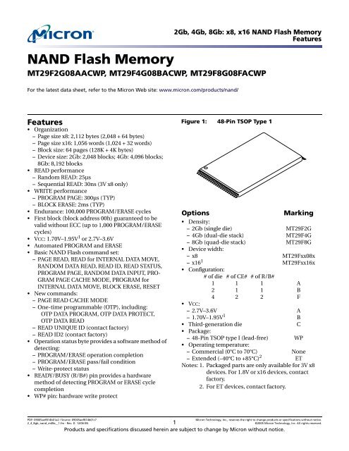
2Gb, 4Gb, 8Gb: x8, x16 <strong>NAND</strong> <strong>Flash</strong> MemoryFeatures<strong>NAND</strong> <strong>Flash</strong> MemoryMT29F2G08AACWP, MT29F4G08BACWP, MT29F8G08FACWPFor the latest data sheet, refer to the <strong>Micron</strong> Web site: www.micron.com/products/nand/Features• Organization– Page size x8: 2,112 bytes (2,048 + 64 bytes)– Page size x16: 1,056 words (1,024 + 32 words)– Block size: 64 pages (128K + 4K bytes)– Device size: 2Gb: 2,048 blocks; 4Gb: 4,096 blocks;8Gb: 8,192 blocks• READ performance– Random READ: 25µs– Sequential READ: 30ns (3V x8 only)• WRITE performance– PROGRAM PAGE: 300µs (TYP)– BLOCK ERASE: 2ms (TYP)• Endurance: 100,000 PROGRAM/ERASE cycles• First block (block address 00h) guaranteed to bevalid without ECC (up to 1,000 PROGRAM/ERASEcycles)• VCC: 1.70V–1.95V 1 or 2.7V–3.6V• Automated PROGRAM and ERASE• Basic <strong>NAND</strong> <strong>Flash</strong> command set:– PAGE READ, READ for INTERNAL DATA MOVE,RANDOM DATA READ, READ ID, READ STATUS,PROGRAM PAGE, RANDOM DATA INPUT, PRO-GRAM PAGE CACHE MODE, PROGRAM forINTERNAL DATA MOVE, BLOCK ERASE, RESET• New commands:– PAGE READ CACHE MODE– One-time programmable (OTP), including:OTP DATA PROGRAM, OTP DATA PROTECT,OTP DATA READ– READ UNIQUE ID (contact factory)– READ ID2 (contact factory)• Operation status byte provides a software method ofdetecting:– PROGRAM/ERASE operation completion– PROGRAM/ERASE pass/fail condition– Write-protect status• READY/BUSY (R/B#) pin provides a hardwaremethod of detecting PROGRAM or ERASE cyclecompletion• WP# pin: hardware write protectFigure 1: 48-Pin TSOP Type 1OptionsMarking• Density:– 2Gb (single die) MT29F2G– 4Gb (dual-die stack) MT29F4G– 8Gb (quad-die stack) MT29F8G• Device width:– x8 MT29Fxx08x– x16 1 MT29Fxx16x• Configuration:# of die # of CE# # of R/B#1 1 1 A2 1 1 B4 2 2 F• VCC:– 2.7V–3.6V A– 1.70V–1.95V 1 B• Third-generation die C• Package:– 48-Pin TSOP type I (lead-free) WP• Operating temperature:– Commercial (0°C to 70°C) None– Extended (–40°C to +85°C) 2 ETNotes: 1. Packaged parts are only available for 3V x8devices. For 1.8V or x16 devices, contactfactory.2. For ET devices, contact factory.PDF: 09005aef814b01a2 / Source: 09005aef814b01c7<strong>Micron</strong> Technology, Inc., reserves the right to change products or specifications without notice.2_4_8gb_nand_m49a__1.fm - Rev. D 12/06 EN 1 ©2005 <strong>Micron</strong> Technology, Inc. All rights reserved.Products and specifications discussed herein are subject to change by <strong>Micron</strong> without notice.
2Gb, 4Gb, 8Gb: x8, x16 <strong>NAND</strong> <strong>Flash</strong> MemoryPart Numbering InformationPart Numbering Information<strong>Micron</strong> ® <strong>NAND</strong> <strong>Flash</strong> devices are available in several different configurations anddensities (see Figure 2).Figure 2:Part Number Chart<strong>Micron</strong> TechnologyMT 29F 2G 08 A A C WP ES :CDesign RevisionC = First generationProduct Family29F = Single-supply <strong>NAND</strong> <strong>Flash</strong> memoryDensity2G = 2Gb4G = 4Gb8G = 8GbDevice Width08 = 8 bits16 = 16 bitsClassification# of die # of CE# # of R/B# I/OA 1 1 1 CommonB 2 1 1 CommonF 4 1 1 CommonOperating Voltage RangeA = 3.3V (2.70V–3.60V)B = 1.8V (1.70V–1.95V)Production StatusBlank = ProductionES = Engineering sampleMS = Mechanical sampleQS = Qualification sampleOperating Temperature RangeBlank = Commercial (0°C to +70°C)ET = Extended (–40°C to +85°C)Reserved for Future Use<strong>Flash</strong> PerformanceBlank = StandardPackage CodesWP = 48-pin TSOP I (lead-free)Feature SetA = First-generation dieB = Second-generation dieC = Third-generation dieValid Part Number CombinationsAfter building the part number from the part numbering chart above, verify that the partnumber is valid using the <strong>Micron</strong> Parametric Part Search at www.micron.com/products/parametric.If the device required is not on this list, contact the factory.PDF: 09005aef814b01a2 / Source: 09005aef814b01c7<strong>Micron</strong> Technology, Inc., reserves the right to change products or specifications without notice.2_4_8gb_nand_m49a__1.fm - Rev. D 12/06 EN 2 ©2005 <strong>Micron</strong> Technology, Inc. All rights reserved.
Table of Contents2Gb, 4Gb, 8Gb: x8, x16 <strong>NAND</strong> <strong>Flash</strong> MemoryTable of ContentsFeatures. . . . . . . . . . . . . . . . . . . . . . . . . . . . . . . . . . . . . . . . . . . . . . . . . . . . . . . . . . . . . . . . . . . . . . . . . . . . . . . . . . . . . . . . .1Part Numbering Information . . . . . . . . . . . . . . . . . . . . . . . . . . . . . . . . . . . . . . . . . . . . . . . . . . . . . . . . . . . . . . . . . . . . . .2Valid Part Number Combinations . . . . . . . . . . . . . . . . . . . . . . . . . . . . . . . . . . . . . . . . . . . . . . . . . . . . . . . . . . . . . . .2General Description . . . . . . . . . . . . . . . . . . . . . . . . . . . . . . . . . . . . . . . . . . . . . . . . . . . . . . . . . . . . . . . . . . . . . . . . . . . . . .6Pin Assignments and Descriptions . . . . . . . . . . . . . . . . . . . . . . . . . . . . . . . . . . . . . . . . . . . . . . . . . . . . . . . . . . . . . . . . .7Architecture . . . . . . . . . . . . . . . . . . . . . . . . . . . . . . . . . . . . . . . . . . . . . . . . . . . . . . . . . . . . . . . . . . . . . . . . . . . . . . . . . . . . .9Addressing . . . . . . . . . . . . . . . . . . . . . . . . . . . . . . . . . . . . . . . . . . . . . . . . . . . . . . . . . . . . . . . . . . . . . . . . . . . . . . . . . . . . . .9Memory Mapping . . . . . . . . . . . . . . . . . . . . . . . . . . . . . . . . . . . . . . . . . . . . . . . . . . . . . . . . . . . . . . . . . . . . . . . . . . . . . . .10Bus Operation . . . . . . . . . . . . . . . . . . . . . . . . . . . . . . . . . . . . . . . . . . . . . . . . . . . . . . . . . . . . . . . . . . . . . . . . . . . . . . . . . .16Control Signals . . . . . . . . . . . . . . . . . . . . . . . . . . . . . . . . . . . . . . . . . . . . . . . . . . . . . . . . . . . . . . . . . . . . . . . . . . . . . . .16Commands . . . . . . . . . . . . . . . . . . . . . . . . . . . . . . . . . . . . . . . . . . . . . . . . . . . . . . . . . . . . . . . . . . . . . . . . . . . . . . . . . .16Address Input . . . . . . . . . . . . . . . . . . . . . . . . . . . . . . . . . . . . . . . . . . . . . . . . . . . . . . . . . . . . . . . . . . . . . . . . . . . . . . . .16Data Input . . . . . . . . . . . . . . . . . . . . . . . . . . . . . . . . . . . . . . . . . . . . . . . . . . . . . . . . . . . . . . . . . . . . . . . . . . . . . . . . . . .17READs . . . . . . . . . . . . . . . . . . . . . . . . . . . . . . . . . . . . . . . . . . . . . . . . . . . . . . . . . . . . . . . . . . . . . . . . . . . . . . . . . . . . . . .17Ready/Busy# . . . . . . . . . . . . . . . . . . . . . . . . . . . . . . . . . . . . . . . . . . . . . . . . . . . . . . . . . . . . . . . . . . . . . . . . . . . . . . . . .17Command Definitions . . . . . . . . . . . . . . . . . . . . . . . . . . . . . . . . . . . . . . . . . . . . . . . . . . . . . . . . . . . . . . . . . . . . . . . . . . .20READ Operations . . . . . . . . . . . . . . . . . . . . . . . . . . . . . . . . . . . . . . . . . . . . . . . . . . . . . . . . . . . . . . . . . . . . . . . . . . . . .21PAGE READ 00h-30h. . . . . . . . . . . . . . . . . . . . . . . . . . . . . . . . . . . . . . . . . . . . . . . . . . . . . . . . . . . . . . . . . . . . . . . .21RANDOM DATA READ 05h-E0h. . . . . . . . . . . . . . . . . . . . . . . . . . . . . . . . . . . . . . . . . . . . . . . . . . . . . . . . . . . . . .22PAGE READ CACHE MODE Start 31h; PAGE READ CACHE MODE Start Last 3Fh . . . . . . . . . . . . . . . . .22READ ID 90h . . . . . . . . . . . . . . . . . . . . . . . . . . . . . . . . . . . . . . . . . . . . . . . . . . . . . . . . . . . . . . . . . . . . . . . . . . . . . . .24READ STATUS 70h . . . . . . . . . . . . . . . . . . . . . . . . . . . . . . . . . . . . . . . . . . . . . . . . . . . . . . . . . . . . . . . . . . . . . . . . .26PROGRAM Operations . . . . . . . . . . . . . . . . . . . . . . . . . . . . . . . . . . . . . . . . . . . . . . . . . . . . . . . . . . . . . . . . . . . . . . . .27PROGRAM PAGE 80h-10h . . . . . . . . . . . . . . . . . . . . . . . . . . . . . . . . . . . . . . . . . . . . . . . . . . . . . . . . . . . . . . . . . . .27SERIAL DATA INPUT 80h . . . . . . . . . . . . . . . . . . . . . . . . . . . . . . . . . . . . . . . . . . . . . . . . . . . . . . . . . . . . . . . . . . .27RANDOM DATA INPUT 85h . . . . . . . . . . . . . . . . . . . . . . . . . . . . . . . . . . . . . . . . . . . . . . . . . . . . . . . . . . . . . . . . .27PROGRAM PAGE CACHE MODE 80h-15h. . . . . . . . . . . . . . . . . . . . . . . . . . . . . . . . . . . . . . . . . . . . . . . . . . . . .28Internal Data Move . . . . . . . . . . . . . . . . . . . . . . . . . . . . . . . . . . . . . . . . . . . . . . . . . . . . . . . . . . . . . . . . . . . . . . . . . . .29READ FOR INTERNAL DATA MOVE 00h-35h . . . . . . . . . . . . . . . . . . . . . . . . . . . . . . . . . . . . . . . . . . . . . . . . . .29PROGRAM for INTERNAL DATA MOVE 85h-10h. . . . . . . . . . . . . . . . . . . . . . . . . . . . . . . . . . . . . . . . . . . . . . .29BLOCK ERASE Operation . . . . . . . . . . . . . . . . . . . . . . . . . . . . . . . . . . . . . . . . . . . . . . . . . . . . . . . . . . . . . . . . . . . . . .31BLOCK ERASE 60h-D0h . . . . . . . . . . . . . . . . . . . . . . . . . . . . . . . . . . . . . . . . . . . . . . . . . . . . . . . . . . . . . . . . . . . . .31One-Time Programmable (OTP) Area . . . . . . . . . . . . . . . . . . . . . . . . . . . . . . . . . . . . . . . . . . . . . . . . . . . . . . . . . . .32OTP DATA PROGRAM A0h-10h . . . . . . . . . . . . . . . . . . . . . . . . . . . . . . . . . . . . . . . . . . . . . . . . . . . . . . . . . . . . . .32OTP DATA PROTECT A5h-10h . . . . . . . . . . . . . . . . . . . . . . . . . . . . . . . . . . . . . . . . . . . . . . . . . . . . . . . . . . . . . . .34OTP DATA READ AFh-30h. . . . . . . . . . . . . . . . . . . . . . . . . . . . . . . . . . . . . . . . . . . . . . . . . . . . . . . . . . . . . . . . . . .35RESET Operation . . . . . . . . . . . . . . . . . . . . . . . . . . . . . . . . . . . . . . . . . . . . . . . . . . . . . . . . . . . . . . . . . . . . . . . . . . . . .36RESET FFh. . . . . . . . . . . . . . . . . . . . . . . . . . . . . . . . . . . . . . . . . . . . . . . . . . . . . . . . . . . . . . . . . . . . . . . . . . . . . . . . .36WRITE PROTECT Operation . . . . . . . . . . . . . . . . . . . . . . . . . . . . . . . . . . . . . . . . . . . . . . . . . . . . . . . . . . . . . . . . . . .37Error Management . . . . . . . . . . . . . . . . . . . . . . . . . . . . . . . . . . . . . . . . . . . . . . . . . . . . . . . . . . . . . . . . . . . . . . . . . . . . . .38Electrical Characteristics . . . . . . . . . . . . . . . . . . . . . . . . . . . . . . . . . . . . . . . . . . . . . . . . . . . . . . . . . . . . . . . . . . . . . . . . .39VCC Power Cycling . . . . . . . . . . . . . . . . . . . . . . . . . . . . . . . . . . . . . . . . . . . . . . . . . . . . . . . . . . . . . . . . . . . . . . . . . . . .39Timing Diagrams. . . . . . . . . . . . . . . . . . . . . . . . . . . . . . . . . . . . . . . . . . . . . . . . . . . . . . . . . . . . . . . . . . . . . . . . . . . . . . . .44Package Dimensions . . . . . . . . . . . . . . . . . . . . . . . . . . . . . . . . . . . . . . . . . . . . . . . . . . . . . . . . . . . . . . . . . . . . . . . . . . . .57PDF: 09005aef814b01a2 / Source: 09005aef814b01c7<strong>Micron</strong> Technology, Inc., reserves the right to change products or specifications without notice.2_4_8gb_nand_m49aTOC.fm - Rev. D 12/06 EN 3 ©2005 <strong>Micron</strong> Technology, Inc. All rights reserved.
List of Figures2Gb, 4Gb, 8Gb: x8, x16 <strong>NAND</strong> <strong>Flash</strong> MemoryList of FiguresFigure 1: 48-Pin TSOP Type 1 . . . . . . . . . . . . . . . . . . . . . . . . . . . . . . . . . . . . . . . . . . . . . . . . . . . . . . . . . . . . . . . . . . . . 1Figure 2: Part Number Chart . . . . . . . . . . . . . . . . . . . . . . . . . . . . . . . . . . . . . . . . . . . . . . . . . . . . . . . . . . . . . . . . . . . . 2Figure 3: <strong>NAND</strong> <strong>Flash</strong> Functional Block Diagram . . . . . . . . . . . . . . . . . . . . . . . . . . . . . . . . . . . . . . . . . . . . . . . . . . 6Figure 4: 48-Pin TSOP Type 1 Pin Assignments (Top View) . . . . . . . . . . . . . . . . . . . . . . . . . . . . . . . . . . . . . . . . . 7Figure 5: Memory Map x8 . . . . . . . . . . . . . . . . . . . . . . . . . . . . . . . . . . . . . . . . . . . . . . . . . . . . . . . . . . . . . . . . . . . . . . 10Figure 6: Memory Map x16 . . . . . . . . . . . . . . . . . . . . . . . . . . . . . . . . . . . . . . . . . . . . . . . . . . . . . . . . . . . . . . . . . . . . . 11Figure 7: Array Organization for MT29F2G08AxC (x8) . . . . . . . . . . . . . . . . . . . . . . . . . . . . . . . . . . . . . . . . . . . . . 12Figure 8: Array Organization for MT29F2G16AxC (x16) . . . . . . . . . . . . . . . . . . . . . . . . . . . . . . . . . . . . . . . . . . . . 13Figure 9: Array Organization for MT29F4G08BxC and MT29F8G08FxC (x8) . . . . . . . . . . . . . . . . . . . . . . . . . . 14Figure 10: Array Organization for MT28F4G16BxC and MT29F8G16FxC (x16) . . . . . . . . . . . . . . . . . . . . . . . . . 15Figure 11: READY/BUSY# Open Drain . . . . . . . . . . . . . . . . . . . . . . . . . . . . . . . . . . . . . . . . . . . . . . . . . . . . . . . . . . . . 18Figure 12: tFall and tRise . . . . . . . . . . . . . . . . . . . . . . . . . . . . . . . . . . . . . . . . . . . . . . . . . . . . . . . . . . . . . . . . . . . . . . . . 18Figure 13: Iol vs. Rp . . . . . . . . . . . . . . . . . . . . . . . . . . . . . . . . . . . . . . . . . . . . . . . . . . . . . . . . . . . . . . . . . . . . . . . . . . . . . 19Figure 14: PAGE READ Operation . . . . . . . . . . . . . . . . . . . . . . . . . . . . . . . . . . . . . . . . . . . . . . . . . . . . . . . . . . . . . . . . 21Figure 15: RANDOM DATA READ Operation . . . . . . . . . . . . . . . . . . . . . . . . . . . . . . . . . . . . . . . . . . . . . . . . . . . . . . 22Figure 16: PAGE READ CACHE MODE . . . . . . . . . . . . . . . . . . . . . . . . . . . . . . . . . . . . . . . . . . . . . . . . . . . . . . . . . . . . 23Figure 17: READ ID Operation . . . . . . . . . . . . . . . . . . . . . . . . . . . . . . . . . . . . . . . . . . . . . . . . . . . . . . . . . . . . . . . . . . . 24Figure 18: Status Register Operation . . . . . . . . . . . . . . . . . . . . . . . . . . . . . . . . . . . . . . . . . . . . . . . . . . . . . . . . . . . . . 26Figure 19: PROGRAM and READ STATUS Operation . . . . . . . . . . . . . . . . . . . . . . . . . . . . . . . . . . . . . . . . . . . . . . . 27Figure 20: RANDOM DATA INPUT . . . . . . . . . . . . . . . . . . . . . . . . . . . . . . . . . . . . . . . . . . . . . . . . . . . . . . . . . . . . . . . 27Figure 21: PROGRAM PAGE CACHE MODE Example . . . . . . . . . . . . . . . . . . . . . . . . . . . . . . . . . . . . . . . . . . . . . . 28Figure 22: INTERNAL DATA MOVE . . . . . . . . . . . . . . . . . . . . . . . . . . . . . . . . . . . . . . . . . . . . . . . . . . . . . . . . . . . . . . 30Figure 23: INTERNAL DATA MOVE with RANDOM DATA INPUT . . . . . . . . . . . . . . . . . . . . . . . . . . . . . . . . . . . 30Figure 24: BLOCK ERASE Operation . . . . . . . . . . . . . . . . . . . . . . . . . . . . . . . . . . . . . . . . . . . . . . . . . . . . . . . . . . . . . . 31Figure 25: OTP DATA PROGRAM . . . . . . . . . . . . . . . . . . . . . . . . . . . . . . . . . . . . . . . . . . . . . . . . . . . . . . . . . . . . . . . . 33Figure 26: OTP DATA PROTECT . . . . . . . . . . . . . . . . . . . . . . . . . . . . . . . . . . . . . . . . . . . . . . . . . . . . . . . . . . . . . . . . . 34Figure 27: OTP DATA READ . . . . . . . . . . . . . . . . . . . . . . . . . . . . . . . . . . . . . . . . . . . . . . . . . . . . . . . . . . . . . . . . . . . . . 35Figure 28: RESET Operation . . . . . . . . . . . . . . . . . . . . . . . . . . . . . . . . . . . . . . . . . . . . . . . . . . . . . . . . . . . . . . . . . . . . . 36Figure 29: ERASE Enable . . . . . . . . . . . . . . . . . . . . . . . . . . . . . . . . . . . . . . . . . . . . . . . . . . . . . . . . . . . . . . . . . . . . . . . . 37Figure 30: ERASE Disable . . . . . . . . . . . . . . . . . . . . . . . . . . . . . . . . . . . . . . . . . . . . . . . . . . . . . . . . . . . . . . . . . . . . . . . 37Figure 31: PROGRAM Enable . . . . . . . . . . . . . . . . . . . . . . . . . . . . . . . . . . . . . . . . . . . . . . . . . . . . . . . . . . . . . . . . . . . . 37Figure 32: PROGRAM Disable . . . . . . . . . . . . . . . . . . . . . . . . . . . . . . . . . . . . . . . . . . . . . . . . . . . . . . . . . . . . . . . . . . . 38Figure 33: AC Waveforms During Power Transitions . . . . . . . . . . . . . . . . . . . . . . . . . . . . . . . . . . . . . . . . . . . . . . . 39Figure 34: COMMAND LATCH Cycle . . . . . . . . . . . . . . . . . . . . . . . . . . . . . . . . . . . . . . . . . . . . . . . . . . . . . . . . . . . . . 44Figure 35: ADDRESS LATCH Cycle . . . . . . . . . . . . . . . . . . . . . . . . . . . . . . . . . . . . . . . . . . . . . . . . . . . . . . . . . . . . . . . 44Figure 36: INPUT DATA LATCH Cycle . . . . . . . . . . . . . . . . . . . . . . . . . . . . . . . . . . . . . . . . . . . . . . . . . . . . . . . . . . . . 45Figure 37: SERIAL ACCESS Cycle After READ . . . . . . . . . . . . . . . . . . . . . . . . . . . . . . . . . . . . . . . . . . . . . . . . . . . . . . 45Figure 38: READ STATUS Cycle . . . . . . . . . . . . . . . . . . . . . . . . . . . . . . . . . . . . . . . . . . . . . . . . . . . . . . . . . . . . . . . . . . 46Figure 39: PAGE READ Operation . . . . . . . . . . . . . . . . . . . . . . . . . . . . . . . . . . . . . . . . . . . . . . . . . . . . . . . . . . . . . . . . 46Figure 40: PAGE READ Operation with CE# “Don’t Care” . . . . . . . . . . . . . . . . . . . . . . . . . . . . . . . . . . . . . . . . . . . 47Figure 41: RANDOM DATA READ Operation . . . . . . . . . . . . . . . . . . . . . . . . . . . . . . . . . . . . . . . . . . . . . . . . . . . . . . 47Figure 42: PAGE READ CACHE MODE Operation, Part 1 of 2 . . . . . . . . . . . . . . . . . . . . . . . . . . . . . . . . . . . . . . . . 48Figure 43: PAGE READ CACHE MODE Operation, Part 2 of 2 . . . . . . . . . . . . . . . . . . . . . . . . . . . . . . . . . . . . . . . . 49Figure 44: PAGE READ CACHE MODE Operation without R/B#, Part 1 of 2 . . . . . . . . . . . . . . . . . . . . . . . . . . . 50Figure 45: PAGE READ CACHE MODE Operation without R/B#, Part 2 of 2 . . . . . . . . . . . . . . . . . . . . . . . . . . . 51Figure 46: READ ID Operation . . . . . . . . . . . . . . . . . . . . . . . . . . . . . . . . . . . . . . . . . . . . . . . . . . . . . . . . . . . . . . . . . . . 52Figure 47: PROGRAM PAGE Operation . . . . . . . . . . . . . . . . . . . . . . . . . . . . . . . . . . . . . . . . . . . . . . . . . . . . . . . . . . . 52Figure 48: PROGRAM PAGE Operation with CE# “Don’t Care” . . . . . . . . . . . . . . . . . . . . . . . . . . . . . . . . . . . . . . 53Figure 49: PROGRAM PAGE Operation with RANDOM DATA INPUT . . . . . . . . . . . . . . . . . . . . . . . . . . . . . . . . 53Figure 50: INTERNAL DATA MOVE Operation . . . . . . . . . . . . . . . . . . . . . . . . . . . . . . . . . . . . . . . . . . . . . . . . . . . . . 54Figure 51: PROGRAM PAGE CACHE MODE Operation . . . . . . . . . . . . . . . . . . . . . . . . . . . . . . . . . . . . . . . . . . . . . 54Figure 52: PROGRAM PAGE CACHE MODE Operation Ending on 15h . . . . . . . . . . . . . . . . . . . . . . . . . . . . . . . 55Figure 53: BLOCK ERASE Operation . . . . . . . . . . . . . . . . . . . . . . . . . . . . . . . . . . . . . . . . . . . . . . . . . . . . . . . . . . . . . . 56Figure 54: RESET Operation . . . . . . . . . . . . . . . . . . . . . . . . . . . . . . . . . . . . . . . . . . . . . . . . . . . . . . . . . . . . . . . . . . . . . 56Figure 55: TSOP Type I . . . . . . . . . . . . . . . . . . . . . . . . . . . . . . . . . . . . . . . . . . . . . . . . . . . . . . . . . . . . . . . . . . . . . . . . . . 57PDF: 09005aef814b01a2 / Source: 09005aef814b01c7<strong>Micron</strong> Technology, Inc., reserves the right to change products or specifications without notice.2_4_8gb_nand_m49aLOF.fm - Rev. D 12/06 EN 4 ©2005 <strong>Micron</strong> Technology, Inc. All rights reserved.
List of Tables2Gb, 4Gb, 8Gb: x8, x16 <strong>NAND</strong> <strong>Flash</strong> MemoryList of TablesTable 1: Pin Descriptions . . . . . . . . . . . . . . . . . . . . . . . . . . . . . . . . . . . . . . . . . . . . . . . . . . . . . . . . . . . . . . . . . . . . . . . 8Table 2: Operational Example (x8) . . . . . . . . . . . . . . . . . . . . . . . . . . . . . . . . . . . . . . . . . . . . . . . . . . . . . . . . . . . . . . 10Table 3: Operational Example (x16) . . . . . . . . . . . . . . . . . . . . . . . . . . . . . . . . . . . . . . . . . . . . . . . . . . . . . . . . . . . . . 11Table 4: Array Addressing: MT29F2G08AxC . . . . . . . . . . . . . . . . . . . . . . . . . . . . . . . . . . . . . . . . . . . . . . . . . . . . . . 12Table 5: Array Addressing: MT29F2G16AxC . . . . . . . . . . . . . . . . . . . . . . . . . . . . . . . . . . . . . . . . . . . . . . . . . . . . . . 13Table 6: Array Addressing for MT29F4G08BxC and MT29F8G08FxC (x8) . . . . . . . . . . . . . . . . . . . . . . . . . . . . 14Table 7: Array Addressing for MT28F4G16BxC and MT29F8G16FxC (x16) . . . . . . . . . . . . . . . . . . . . . . . . . . . 15Table 8: Mode Selection . . . . . . . . . . . . . . . . . . . . . . . . . . . . . . . . . . . . . . . . . . . . . . . . . . . . . . . . . . . . . . . . . . . . . . . 19Table 9: Command Set . . . . . . . . . . . . . . . . . . . . . . . . . . . . . . . . . . . . . . . . . . . . . . . . . . . . . . . . . . . . . . . . . . . . . . . . 20Table 10: Device ID and Configuration Codes. . . . . . . . . . . . . . . . . . . . . . . . . . . . . . . . . . . . . . . . . . . . . . . . . . . . . 25Table 11: Status Register Bit Definition . . . . . . . . . . . . . . . . . . . . . . . . . . . . . . . . . . . . . . . . . . . . . . . . . . . . . . . . . . . 26Table 12: Status Register Contents After RESET Operation . . . . . . . . . . . . . . . . . . . . . . . . . . . . . . . . . . . . . . . . . 36Table 13: Absolute Maximum Ratings by Device . . . . . . . . . . . . . . . . . . . . . . . . . . . . . . . . . . . . . . . . . . . . . . . . . . 39Table 14: Recommended Operating Conditions . . . . . . . . . . . . . . . . . . . . . . . . . . . . . . . . . . . . . . . . . . . . . . . . . . . 39Table 15: M29FxGxxxAC 3V Device DC and Operating Characteristics . . . . . . . . . . . . . . . . . . . . . . . . . . . . . . . 40Table 16: M29FxGxxxBC 1.8V Device DC and Operating Characteristics . . . . . . . . . . . . . . . . . . . . . . . . . . . . . 41Table 17: Valid Blocks . . . . . . . . . . . . . . . . . . . . . . . . . . . . . . . . . . . . . . . . . . . . . . . . . . . . . . . . . . . . . . . . . . . . . . . . . . 41Table 18: Capacitance . . . . . . . . . . . . . . . . . . . . . . . . . . . . . . . . . . . . . . . . . . . . . . . . . . . . . . . . . . . . . . . . . . . . . . . . . . 42Table 19: Test Conditions . . . . . . . . . . . . . . . . . . . . . . . . . . . . . . . . . . . . . . . . . . . . . . . . . . . . . . . . . . . . . . . . . . . . . . . 42Table 20: AC Characteristics: Command, Data, and Address Input . . . . . . . . . . . . . . . . . . . . . . . . . . . . . . . . . . 42Table 21: AC Characteristics: Normal Operation. . . . . . . . . . . . . . . . . . . . . . . . . . . . . . . . . . . . . . . . . . . . . . . . . . . 43Table 22: PROGRAM/ERASE Characteristics . . . . . . . . . . . . . . . . . . . . . . . . . . . . . . . . . . . . . . . . . . . . . . . . . . . . . . 43PDF: 09005aef814b01a2 / Source: 09005aef814b01c7<strong>Micron</strong> Technology, Inc., reserves the right to change products or specifications without notice.2_4_8gb_nand_m49aLOT.fm - Rev. D 12/06 EN 5 ©2005 <strong>Micron</strong> Technology, Inc. All rights reserved.
2Gb, 4Gb, 8Gb: x8, x16 <strong>NAND</strong> <strong>Flash</strong> MemoryGeneral DescriptionGeneral Description<strong>NAND</strong> <strong>Flash</strong> technology provides a cost-effective solution for applications requiringhigh-density, solid-state storage. <strong>Micron</strong> MT29F2G08AxC and MT29F2G16AxC devicesare 2Gb <strong>NAND</strong> <strong>Flash</strong> memory devices. The MT29F4G08BxC and MT29F4G16BxC are4Gb devices. The MT29F8G08FAC is a four-die stack that operates as two independent4Gb devices, providing a total storage capacity of 8Gb in a single, space-saving package.These devices include standard <strong>NAND</strong> <strong>Flash</strong> features as well as new features designed toenhance system-level performance.<strong>Micron</strong> <strong>NAND</strong> <strong>Flash</strong> devices use a highly multiplexed 8- or 16-bit bus (I/O[7:0] orI/O[15:0]) to transfer data, addresses, and instructions. The five command pins (CLE,ALE, CE#, RE#, WE#) implement the <strong>NAND</strong> <strong>Flash</strong> command bus interface protocol. Twoadditional pins control hardware write protection (WP#) and monitor device status(R/B#).This hardware interface creates a low-pin-count device with a standard pinout that isthe same from one density to another, supporting future upgrades to higher densitieswithout board redesign.The MT29F2G and MT29F4G devices contain 2,048 and 4,096 erasable blocks, respectively.Each block is subdivided into 64 programmable pages. Each page consists of2,112 bytes (x8) or 1,056 words (x16). The pages are further divided into a 2,048-byte datastorage region with a separate 64-byte area on the x8 device; and on the x16 device, separate1,024-word and 32-word areas. The 64-byte and 32-word areas are typically usedfor error management functions.The contents of each 2,112-byte page can be programmed in 300µs, and an entire 132Kbyte/66K-wordblock can be erased in 2ms. On-chip control logic automates PROGRAMand ERASE operations to maximize cycle endurance. ERASE/PROGRAM endurance isspecified at 100,000 cycles when appropriate error correction code (ECC) and errormanagement are used.Figure 3:<strong>NAND</strong> <strong>Flash</strong> Functional Block DiagramVCCVSSI/O [7:0]I/O [15:0]I/OControlAddress RegisterStatus RegisterCommand RegisterCE#CLEALEWE#RE#WP#ControlLogicRow DecodeColumn DecodeR/B#Data RegisterCache RegisterPDF: 09005aef814b01a2 / Source: 09005aef814b01c7<strong>Micron</strong> Technology, Inc., reserves the right to change products or specifications without notice.2_4_8gb_nand_m49a__2.fm - Rev. D 12/06 EN 6 ©2005 <strong>Micron</strong> Technology, Inc. All rights reserved.
2Gb, 4Gb, 8Gb: x8, x16 <strong>NAND</strong> <strong>Flash</strong> MemoryPin Assignments and DescriptionsPin Assignments and DescriptionsFigure 4:48-Pin TSOP Type 1 Pin Assignments (Top View)x16x8x8x16NCNCNCNCNCR/B2# 1R/B#RE#CE#CE2# 1NCVCCVSSNCNCCLEALEWE#WP#DNUDNUDNUNCNCNCNCNCNCNCR/B2# 1R/B#RE#CE#CE2# 1NCVCCVSSNCNCCLEALEWE#WP#DNUDNUDNUNCNC1 ●23456789101112131415161718192021222324484746454443424140393837363534333231302928272625NCNCNCNCI/O7I/O6I/O5I/O4NCNCDNU or VSSVCCVSSNCNCNCI/O3I/O2I/O1I/O0NCNCNCNCVSSI/O15I/O7I/O14I/O6I/O13I/O5I/O12I/O4NCDNU or VSSVCCNCNCNCI/O11I/O3I/O10I/O2I/O9I/O1I/O8I/O0VSSNotes: 1. R/B2# and CE2# are available only on 8Gb devices. These pins are NC for otherconfigurations.PDF: 09005aef814b01a2 / Source: 09005aef814b01c7<strong>Micron</strong> Technology, Inc., reserves the right to change products or specifications without notice.2_4_8gb_nand_m49a__2.fm - Rev. D 12/06 EN 7 ©2005 <strong>Micron</strong> Technology, Inc. All rights reserved.
2Gb, 4Gb, 8Gb: x8, x16 <strong>NAND</strong> <strong>Flash</strong> MemoryPin Assignments and DescriptionsTable 1:Pin DescriptionsSymbol Type DescriptionALE Input Address latch enable: During the time ALE is HIGH, address information istransferred from I/O[7:0] into the on-chip address register upon a LOW-to-HIGHtransition on WE#. When address information is not being loaded, the ALE pinshould be driven LOW.CE#, CE2# Input Chip enable: This gates transfers between the host system and the <strong>NAND</strong> <strong>Flash</strong>device. Once the device starts a PROGRAM or ERASE operation, the chip enablepin can be de-asserted.For the 8Gb configuration, CE# controls the first 4Gb of memory; CE2# controlsthe second 4Gb. See “Bus Operation” on page 16 for additional operationaldetails.In the 8Gb configuration, R/B# is for the 4Gb of memory enabled by CE#; R/B2# isfor the 4Gb of memory enabled by the CE2#.CLE Input Command latch enable: When CLE is HIGH, information is transferred fromI/O[7:0] to the on-chip command register on the rising edge of WE#. Whencommand information is not being loaded, CLE should be driven LOW.RE# Input Read enable: This gates transfers from the <strong>NAND</strong> <strong>Flash</strong> device to the host system.WE# Input Write enable: This gates transfers from the host system to the <strong>NAND</strong> <strong>Flash</strong> device.WP# Input Write protect: Pin protects against inadvertent PROGRAM and ERASE operations.All PROGRAM and ERASE operations are disabled when the WP# pin is LOW.I/O[7:0]MT29FxG08I/OI/O[15:0]MT29FxG16Data inputs/outputs: The bidirectional I/O pins transfer address, data, andinstruction information. Data is output only during READ operations; at othertimes the I/O pins are inputs.R/B#, R/B2# Output Ready/busy: An open-drain, active-LOW output that uses an external pull-upresistor, the pin is used to indicate when the chip is processing a PROGRAM orERASE operation. The pin is also used during a READ operation to indicate whendata is being transferred from the array into the serial data register. When theseoperations have completed, the R/B# returns to the High-Z state.VCC Supply VCC: Power supply.VSS Supply VSS: Ground connection.NC – No connect: NC pins are not internally connected. These pins can be driven or leftunconnected.DNU – Do not use: These pins must be left unconnected.PDF: 09005aef814b01a2 / Source: 09005aef814b01c7<strong>Micron</strong> Technology, Inc., reserves the right to change products or specifications without notice.2_4_8gb_nand_m49a__2.fm - Rev. D 12/06 EN 8 ©2005 <strong>Micron</strong> Technology, Inc. All rights reserved.
2Gb, 4Gb, 8Gb: x8, x16 <strong>NAND</strong> <strong>Flash</strong> MemoryArchitectureArchitectureAddressingThese devices use <strong>NAND</strong> <strong>Flash</strong> electrical and command interfaces. Data, commands,and addresses are multiplexed onto the same pins to provide a memory device with alow pin count.The internal memory array is accessed on a page basis. During reads, a page of data iscopied from the memory array into the data register. Once copied to the data register,data is output sequentially, byte by byte on x8 devices, or word by word on x16 devices.The memory array is programmed on a page basis. After the starting address is loadedinto the internal address register, data is sequentially written to the internal data registerup to the end of a page. After all of the page data has been loaded into the data register,array programming is started.In order to increase programming bandwidth, this device incorporates a cache register.In the cache programming mode, data is first copied into the cache register and theninto the data register. When the data is copied into the data register, programmingbegins.After the data register has been loaded and programming has started, the cache registerbecomes available for loading of additional data. Loading of the next page of data intothe cache register takes place while page programming is in process.The INTERNAL DATA MOVE command also uses the internal cache register. Normally,moving data from one area of external memory to another uses a large number of externalmemory cycles. With the use of the internal cache register and data register, arraydata can be copied from one page and then programmed into another without the use ofexternal memory cycles.<strong>NAND</strong> <strong>Flash</strong> devices do not contain dedicated address pins. Addresses are loaded usinga five-cycle sequence, as shown in Tables 4 and 5 on pages 12 and 13. See Figures 5 and 6on pages 10 and 11 for additional memory mapping and addressing details.PDF: 09005aef814b01a2 / Source: 09005aef814b01c7<strong>Micron</strong> Technology, Inc., reserves the right to change products or specifications without notice.2_4_8gb_nand_m49a__2.fm - Rev. D 12/06 EN 9 ©2005 <strong>Micron</strong> Technology, Inc. All rights reserved.
2Gb, 4Gb, 8Gb: x8, x16 <strong>NAND</strong> <strong>Flash</strong> MemoryMemory MappingMemory MappingFigure 5:Memory Map x8BlocksBA[16:6]0 1 2• • • • • • • • • • • •2,047PagesPA[5:0]0 1 2 • • • 63BytesCA[11:0]0 1 2 • • • • • • • • • • • • • • • • • • • 2,047 • • • 2,111Spare areaTable 2:Operational Example (x8)Block Page Min Address in Page Max Address in Page Out-of-Bounds Addresses in Page0 0 0x0000000000 0x000000083F 0x0000000840–0x0000000FFF0 1 0x0000010000 0x000001083F 0x0000010840–0x0000010FFF0 2 0x0000020000 0x000002083F 0x0000020840–0x0000020FFF… … … …2,046 62 0x01FFFE0000 0x01FFFE083F 0x01FFFE0840–0x01FFFE0FFF2,047 63 0x01FFFF0000 0x01FFFF083F 0x01FFFF0840–0x01FFFF0FFFNotes: 1. As shown in Table 4 on page 12, the high nibble of address cycle 2 has no assigned addressbits; however, these 4 bits must be held LOW during the ADDRESS cycle to ensure that theaddress is interpreted correctly by the <strong>NAND</strong> <strong>Flash</strong> device. These extra bits are accountedfor in ADDRESS cycle 2 even though they do not have address bits assigned to them.2. The 12-bit column address is capable of addressing from 0 to 4,095 bytes on x8 devices;however, only bytes 0 through 2,111 are valid. Bytes 2,112 through 4,095 of each pageare “out of bounds,” do not exist in the device, and cannot be addressed.PDF: 09005aef814b01a2 / Source: 09005aef814b01c7<strong>Micron</strong> Technology, Inc., reserves the right to change products or specifications without notice.2_4_8gb_nand_m49a__2.fm - Rev. D 12/06 EN 10 ©2005 <strong>Micron</strong> Technology, Inc. All rights reserved.
2Gb, 4Gb, 8Gb: x8, x16 <strong>NAND</strong> <strong>Flash</strong> MemoryMemory MappingFigure 6:Memory Map x16BlocksBA[16:6]0 1 2• • • • • • • • • • • •2,047PagesPA[5:0]0 1 2 • • • 63WordsCA[10:0]0 1 2 • • • • • • • • • • • • • • • • • • • 1,023 • • • 1,055Spare areaTable 3:Operational Example (x16)Block Page Min Address in Page Max Address in Page Out-of-Bounds Addresses in Page0 0 0x0000000000 0x000000041F 0x0000000420–0x0000000FFF0 1 0x0000010000 0x000001041F 0x0000010420–0x0000010FFF0 2 0x0000020000 0x000002041F 0x0000020420–0x0000020FFF… … … …2,046 62 0x01FFFE0000 0x01FFFE041F 0x01FFFE0420–0x01FFFE0FFF2,047 63 0x01FFFF0000 0x01FFFF041F 0x01FFFF0420–0x01FFFF0FFFNotes: 1. As shown in Table 5 on page 13, the upper 5 bits of address cycle 2 have no assignedaddress bits; however, these 5 bits must be held LOW during the ADDRESS cycle to ensurethat the address is interpreted correctly by the <strong>NAND</strong> <strong>Flash</strong> device. These extra bits areaccounted for in ADDRESS cycle 2 even though they do not have address bits assigned tothem.2. The 11-bit column address is capable of addressing from 0 to 2,047 words on x16 devices;however, only words 0 through 1,055 are valid. Words 1,056 through 2,048 of each pageare “out of bounds,” do not exist in the device, and cannot be addressed.PDF: 09005aef814b01a2 / Source: 09005aef814b01c7<strong>Micron</strong> Technology, Inc., reserves the right to change products or specifications without notice.2_4_8gb_nand_m49a__2.fm - Rev. D 12/06 EN 11 ©2005 <strong>Micron</strong> Technology, Inc. All rights reserved.
2Gb, 4Gb, 8Gb: x8, x16 <strong>NAND</strong> <strong>Flash</strong> MemoryMemory MappingFigure 7:Array Organization for MT29F2G08AxC (x8)2,112 bytesCache Register2,04864I/O 7I/O 0Data Register2,048642,048 blocksper device1 block64 pages = 1 block(128K + 4K) bytes1 page = (2K + 64) bytes1 block = (2K + 64) bytes x 64 pages= (128K + 4K) bytes1 device = (2K + 64) bytes x 64 pagesx 2,048 blocks= 2,112MbTable 4:Array Addressing: MT29F2G08AxCCycle I/O7 I/O6 I/O5 I/O4 I/O3 I/O2 I/O1 I/O0First CA7 CA6 CA5 CA4 CA3 CA2 CA1 CA0Second LOW LOW LOW LOW CA11 1 CA10 CA9 CA8Third BA7 BA6 PA5 PA4 PA3 PA2 PA1 PA0Fourth BA15 BA14 BA13 BA12 BA11 BA10 BA9 BA8Fifth LOW LOW LOW LOW LOW LOW LOW BA16Notes: 1. If CA11 = “1” then CA[10:6] must be “0.”2. Block address concatenated with page address = actual page address; CAx = columnaddress; PAx = page address; BAx = block address.PDF: 09005aef814b01a2 / Source: 09005aef814b01c7<strong>Micron</strong> Technology, Inc., reserves the right to change products or specifications without notice.2_4_8gb_nand_m49a__2.fm - Rev. D 12/06 EN 12 ©2005 <strong>Micron</strong> Technology, Inc. All rights reserved.
2Gb, 4Gb, 8Gb: x8, x16 <strong>NAND</strong> <strong>Flash</strong> MemoryMemory MappingFigure 8:Array Organization for MT29F2G16AxC (x16)1,056 wordsCache Register1,02432I/O 0I/O 15Data Register1,024322,048 blocksper device1 block64 pages = 1 block(64K + 2K) words1 page = (1K + 32) words1 block = (1K + 32) words x 64 pages= (64K + 2K) words1 device = (1K + 32) words x 64 pagesx 2,048 blocks= 2,112MbNote:For x16 devices, contact factory.Table 5:Array Addressing: MT29F2G16AxCCycle I/O[15:8] I/O7 I/O6 I/O5 I/O4 I/O3 I/O2 I/O1 I/O0First LOW CA7 CA6 CA5 CA4 CA3 CA2 CA1 CA0Second LOW LOW LOW LOW LOW LOW CA10 1 CA9 CA8Third LOW BA7 BA6 PA5 PA4 PA3 PA2 PA1 PA0Fourth LOW BA15 BA14 BA13 BA12 BA11 BA10 BA9 BA8Fifth LOW LOW LOW LOW LOW LOW LOW LOW BA16Notes: 1. If CA10 = “1” then CA[9:5] must be “0.”2. Block address concatenated with page address = actual page address. CAx = columnaddress; PAx = page address, BAx = block address.3. I/O[15:8] are not used during the addressing sequence and should be driven LOW.PDF: 09005aef814b01a2 / Source: 09005aef814b01c7<strong>Micron</strong> Technology, Inc., reserves the right to change products or specifications without notice.2_4_8gb_nand_m49a__2.fm - Rev. D 12/06 EN 13 ©2005 <strong>Micron</strong> Technology, Inc. All rights reserved.
2Gb, 4Gb, 8Gb: x8, x16 <strong>NAND</strong> <strong>Flash</strong> MemoryMemory MappingFigure 9:Array Organization for MT29F4G08BxC and MT29F8G08FxC (x8)2,112 bytesCache Register2,04864I/O 7I/O 0Data Register2,048644,096 blocksper device1 block64 pages = 1 block(128K + 4K) bytes1 page = (2K + 64) bytes1 block = (2K + 64) bytes x 64 pages= (128K + 4K) bytes1 device = (2K + 64) bytes x 64 pagesx 4,096 blocks= 4,224MbNote:For the 8Gb MT29F8G08F, the 4Gb array organization shown applies to each chip enable(CE# and CE2#).Table 6:Array Addressing for MT29F4G08BxC and MT29F8G08FxC (x8)Cycle I/O7 I/O6 I/O5 I/O4 I/O3 I/O2 I/O1 I/O0First CA7 CA6 CA5 CA4 CA3 CA2 CA1 CA0Second LOW LOW LOW LOW CA11 1 CA10 CA9 CA8Third BA7 BA6 PA5 PA4 PA3 PA2 PA1 PA0Fourth BA15 BA14 BA13 BA12 BA11 BA10 BA9 BA8Fifth LOW LOW LOW LOW LOW LOW BA17 2 BA16Notes: 1. If CA11 = “1” then CA[10:6] must be “0.”2. Die address boundary: “0” = 0Gb–2Gb devices; “1” = 2Gb–4Gb devices.3. Block address concatenated with page address = actual page address. CAx = columnaddress; PAx = page address; BAx = block address.PDF: 09005aef814b01a2 / Source: 09005aef814b01c7<strong>Micron</strong> Technology, Inc., reserves the right to change products or specifications without notice.2_4_8gb_nand_m49a__2.fm - Rev. D 12/06 EN 14 ©2005 <strong>Micron</strong> Technology, Inc. All rights reserved.
2Gb, 4Gb, 8Gb: x8, x16 <strong>NAND</strong> <strong>Flash</strong> MemoryMemory MappingFigure 10:Array Organization for MT28F4G16BxC and MT29F8G16FxC (x16)1,056 wordsCache Register1,02432I/O 0I/O 15Data Register1,024324,096 blocksper device1 block64 pages = 1 block(64K + 2K) words1 page = (1K + 32) words1 block = (1K + 32) words x 64 pages= (64K + 2K) words1 device = (1K + 32) words x 64 pagesx 4,096 blocks= 4,224MbNotes: 1. For x16 devices, contact factory.2. For the 8Gb MT29F8G16F, the 4Gb array organization shown applies to each chip enable(CE# and CE2#).Table 7:Array Addressing for MT28F4G16BxC and MT29F8G16FxC (x16)Cycle I/O[15:8] I/O7 I/O6 I/O5 I/O4 I/O3 I/O2 I/O1 I/O0First LOW CA7 CA6 CA5 CA4 CA3 CA2 CA1 CA0Second LOW LOW LOW LOW LOW LOW CA10 1 CA9 CA8Third LOW BA7 BA6 PA5 PA4 PA3 PA2 PA1 PA0Fourth LOW BA15 BA14 BA13 BA12 BA11 BA10 BA9 BA8Fifth LOW LOW LOW LOW LOW LOW LOW BA17 2 BA16Notes: 1. If CA10 = “1” then CA[9:5] must be “0.”2. Die address boundary: “0” = 0Gb–2Gb devices, “1” = 2Gb–4Gb devices.3. Block address concatenated with page address = actual page address. CAx = columnaddress; PAx = page address; BAx = block address.4. I/O[15:8] are not used during the addressing sequence and should be driven LOW.PDF: 09005aef814b01a2 / Source: 09005aef814b01c7<strong>Micron</strong> Technology, Inc., reserves the right to change products or specifications without notice.2_4_8gb_nand_m49a__2.fm - Rev. D 12/06 EN 15 ©2005 <strong>Micron</strong> Technology, Inc. All rights reserved.
2Gb, 4Gb, 8Gb: x8, x16 <strong>NAND</strong> <strong>Flash</strong> MemoryBus OperationBus OperationControl SignalsCommandsAddress InputThe bus on the MT29Fxxx devices is multiplexed. Data I/O, addresses, and commandsall share the same pins. I/O pins I/O[15:8] are used only for data in the x16 configuration.Addresses and commands are always supplied on I/O[7:0].The command sequence normally consists of a command latch cycle, an ADDRESSLATCH cycle, and a DATA cycle—either READ or WRITE.CE#, WE#, RE#, CLE, ALE and WP# control <strong>NAND</strong> <strong>Flash</strong> device READ and WRITE operations.On the 8Gb MT29F8G08FAC, CE# and CE2# each control independent 4Gb arrays.CE2# functions the same as CE# for its own array; all operations described for CE# alsoapply to CE2#.CE# is used to enable the device. When CE# is LOW and the device is not in the busystate, the <strong>NAND</strong> <strong>Flash</strong> memory will accept command, data, and address information.When the device is not performing an operation, CE# is typically driven HIGH and thedevice enters standby mode. The memory will enter standby if CE# goes HIGH whiledata is being transferred and the device is not busy. This helps reduce power consumption.See Figure 40 on page 47 and Figure 48 on page 53 for examples of CE# “Don’tCare” operations.The CE# “Don’t Care” operation enables the <strong>NAND</strong> <strong>Flash</strong> to reside on the same asynchronousmemory bus as other <strong>Flash</strong> or SRAM devices. Other devices on the memorybus can then be accessed while the <strong>NAND</strong> <strong>Flash</strong> is busy with internal operations. Thiscapability is important for designs that require multiple <strong>NAND</strong> <strong>Flash</strong> devices on thesame bus. One device can be programmed while another is being read.A HIGH CLE signal indicates that a command cycle is taking place. A HIGH ALE signalsignifies that an address input cycle is occurring.Commands are written to the command register on the rising edge of WE# when:• CE# and ALE are LOW, and• CLE is HIGH, and• the device is not busy.The exceptions to this are the READ STATUS and RESET commands when busy. SeeFigure 34 on page 44 for detailed timing requirements.Commands are input on I/O[7:0] only. For devices with a x16 interface, I/O[15:8] mustbe written with zeros when a command is issued.Addresses are written to the address register on the rising edge of WE# when:• CE# and CLE are LOW, and• ALE is HIGH, and• the device is not busy.Addresses are input on I/O[7:0] only; bits not part of the address space must be LOW.For devices with a x16 interface, I/O[15:8] must be written with zeros when an address isissued.The number of ADDRESS cycles required for each command varies. Refer to the commanddescriptions to determine addressing requirements (see Table 9 on page 20).PDF: 09005aef814b01a2 / Source: 09005aef814b01c7<strong>Micron</strong> Technology, Inc., reserves the right to change products or specifications without notice.2_4_8gb_nand_m49a__2.fm - Rev. D 12/06 EN 16 ©2005 <strong>Micron</strong> Technology, Inc. All rights reserved.
2Gb, 4Gb, 8Gb: x8, x16 <strong>NAND</strong> <strong>Flash</strong> MemoryBus OperationData InputREADsReady/Busy#Data is written to the data register on the rising edge of WE# when:• CE#, CLE, and ALE are LOW, and• the device is not busy.Data is input on I/O[7:0] for x8 devices, and on I/O[15:0] for x16 devices. See Figure 36on page 45 for additional data input details.After a READ command is issued, data is transferred from the memory array to the dataregister on the rising edge of WE#. R/B# goes LOW for t R and transitions HIGH after thetransfer is complete. When R/B# goes HIGH, data is available in the data register; it isclocked out of the part by toggling RE#. See Figure 39 on page 46 for detailed timinginformation.The READ STATUS (70h) command or the R/B# signal can be used to determine whenthe device is ready. See the READ STATUS command section on page 26 for details.The R/B# output provides a hardware method of indicating the completion of PRO-GRAM, ERASE, and READ operations. The signal requires a pull-up resistor for properoperation. The signal is typically HIGH, and transitions to LOW after the appropriatecommand is written to the device. The signal pin’s open-drain driver enables multipleR/B# outputs to be OR-tied. The READ STATUS command can be used in place of R/B#.Typically, R/B# is connected to an interrupt pin on the system controller (see Figure 11on page 18).On the 8Gb MT29F8G08FAC, R/B# provides a status indication for the 4Gb sectionenabled by CE#, and R/B2# does the same for the 4Gb section enabled by CE2#. R/B#and R/B2# can be tied together, or they can be used separately to provide independentindications for each 4Gb section.The combination of Rp and capacitive loading of the R/B# circuit determines the risetime of the R/B# pin. The actual value used for Rp depends on the system timingrequirements. Large values of Rp cause R/B# to be delayed significantly. At the 10 percentto 90 percent points on the R/B# waveform, rise time is approximately two timeconstants (TC).TC = R × CWhere R = Rp (resistance of pull-up resistor), and C = total capacitive load.The fall time of the R/B# signal is determined mainly by the output impedance of theR/B# pin and the total load capacitance.Figure 12 on page 18 and Figure 13 on page 19 depict approximate Rp values using a circuitload of 100pF.The minimum value for Rp is determined by the output drive capability of the R/B# signal,the output voltage swing, and VCC.VCC( MAX) – VOL( MAX)Rp( MIN)---------------------------------------------------------------1.85V= = -------------------------IOL + ΣIL 3mA + ΣILWhere ΣIL is the sum of the input currents of all devices tied to the R/B# pin.PDF: 09005aef814b01a2 / Source: 09005aef814b01c7<strong>Micron</strong> Technology, Inc., reserves the right to change products or specifications without notice.2_4_8gb_nand_m49a__2.fm - Rev. D 12/06 EN 17 ©2005 <strong>Micron</strong> Technology, Inc. All rights reserved.
2Gb, 4Gb, 8Gb: x8, x16 <strong>NAND</strong> <strong>Flash</strong> MemoryBus OperationFigure 11:READY/BUSY# Open DrainRpVCCR/B#Open drain outputIOLGNDDeviceFigure 12:t Fall and t Rise3.503.002.502.00V1.501.000.50t Fallt Rise0.00-1 0 2 4 0 2 4 6TCVcc 3.3Vcc 1.8Notes: 1. t Fall and t Rise are calculated at 10 percent and 90 percent points.2.t Rise is primarily dependent on external pull-up resistor and external capacitive loading.3.t Fall ≈ 10ns at 3.3V; t Fall ≈ 7ns at 1.8V.PDF: 09005aef814b01a2 / Source: 09005aef814b01c7<strong>Micron</strong> Technology, Inc., reserves the right to change products or specifications without notice.2_4_8gb_nand_m49a__2.fm - Rev. D 12/06 EN 18 ©2005 <strong>Micron</strong> Technology, Inc. All rights reserved.
2Gb, 4Gb, 8Gb: x8, x16 <strong>NAND</strong> <strong>Flash</strong> MemoryBus OperationFigure 13:IOL vs. Rp3.503.002.50T (µs)2.001.501.000.500.000 2,000 4,000 6,000 8,000 10,000 12,000Rp (Ω)IOL at 3.60V (mA)IOL at 1.95V (mA)Table 8:Mode SelectionCLE ALE CE# WE# RE# WP# 1 ModeH L L H X Read mode Command inputL H L H X Address inputH L L H H Write mode Command inputL H L H H Address inputL L L H H Data inputL L L H X Sequential read and data outputL L L H H X During read (busy)X X X X X H During program (busy)X X X X X H During erase (busy)X X X X X L Write protectX X H X X 0V/VCC StandbyNotes: 1. WP# should be biased to CMOS HIGH or LOW for standby.2. H = Logic level HIGH; L = Logic level LOW; X = VIH or VIL.PDF: 09005aef814b01a2 / Source: 09005aef814b01c7<strong>Micron</strong> Technology, Inc., reserves the right to change products or specifications without notice.2_4_8gb_nand_m49a__2.fm - Rev. D 12/06 EN 19 ©2005 <strong>Micron</strong> Technology, Inc. All rights reserved.
2Gb, 4Gb, 8Gb: x8, x16 <strong>NAND</strong> <strong>Flash</strong> MemoryCommand DefinitionsCommand DefinitionsTable 9:Command SetNumber ofAddressCyclesDataCyclesRequired 1ValidDuringBusyOperationCommandCycle 1CommandCycle 2NotesPAGE READ 00h 5 No 30h NoPAGE READ CACHE MODE START 31h – No – NoPAGE READ CACHE MODE START LAST 3Fh – No – NoREAD for INTERNAL DATA MOVE 00h 5 No 35h No 2RANDOM DATA READ 05h 2 No E0h No 3READ ID 90h 1 No – NoREAD STATUS 70h – No – YesPROGRAM PAGE 80h 5 Yes 10h NoPROGRAM PAGE CACHE MODE 80h 5 Yes 15h NoPROGRAM for INTERNAL DATA MOVE 85h 5 Optional 10h No 2RANDOM DATA INPUT 85h 2 Yes – No 4BLOCK ERASE 60h 3 No D0h NoRESET FFh – No – YesOTP DATA PROGRAM A0h 5 Yes 10h NoOTP DATA PROTECT A5h 5 No 10h NoOTP DATA READ AFh 5 No 30h NoNotes: 1. Indicates required data cycles between command cycle 1 and command cycle 2.2. Do not cross die boundaries when using READ for INTERNAL DATA MOVE and PROGRAMfor INTERNAL DATA MOVE.3. RANDOM DATA READ command is limited to use within a single page.4. RANDOM DATA INPUT command is limited to use within a single page.PDF: 09005aef814b01a2 / Source: 09005aef814b01c7<strong>Micron</strong> Technology, Inc., reserves the right to change products or specifications without notice.2_4_8gb_nand_m49a__2.fm - Rev. D 12/06 EN 20 ©2005 <strong>Micron</strong> Technology, Inc. All rights reserved.
2Gb, 4Gb, 8Gb: x8, x16 <strong>NAND</strong> <strong>Flash</strong> MemoryCommand DefinitionsREAD OperationsPAGE READ 00h-30hOn initial power-up, the device defaults to read mode. To enter the read mode while inoperation, write the 00h command to the command register, then write five ADDRESScycles followed by the 30h command.To determine the progress of the data transfer from the <strong>NAND</strong> <strong>Flash</strong> array to the dataregister ( t R), monitor the R/B# signal, or, alternatively, issue a READ STATUS (70h) command.If the READ STATUS command is used to monitor the data transfer, the usermust re-issue the READ (00h) command to receive data output from the data register.See Figure 44 on page 50 and Figure 45 on page 51 for examples. After the READ commandhas been re-issued, pulsing the RE# line will result in outputting data, startingfrom the initial column address.A serial page read sequence outputs a complete page of data. After 30h is written, thepage data is transferred to the data register, and R/B# goes LOW during the transfer.When the transfer to the data register is complete, R/B# returns HIGH. At this point, datacan be read from the device. Starting from the initial column address and going to theend of the page, read the data by repeatedly pulsing RE# at the maximum t RC rate (seeFigure 14).Figure 14:PAGE READ OperationCLECE#t WCWE#t WBt CLRt RCt RHZt ARALEt RRE#t RRt RPI/Ox00hColadd 1Coladd 2Rowadd 1Rowadd 2Rowadd 330hDOUTNDOUTN + 1DOUTMBusyR/B#Don’t CarePDF: 09005aef814b01a2 / Source: 09005aef814b01c7<strong>Micron</strong> Technology, Inc., reserves the right to change products or specifications without notice.2_4_8gb_nand_m49a__2.fm - Rev. D 12/06 EN 21 ©2005 <strong>Micron</strong> Technology, Inc. All rights reserved.
2Gb, 4Gb, 8Gb: x8, x16 <strong>NAND</strong> <strong>Flash</strong> MemoryCommand DefinitionsRANDOM DATA READ 05h-E0hThe RANDOM DATA READ command enables the user to specify a new column addressso the data at single or multiple addresses can be read. The random read mode isenabled after a normal PAGE READ (00h-30h) sequence.Random data can be output after the initial page read by writing an 05h-E0h commandsequence along with the new column address (two cycles).The RANDOM DATA READ command can be issued without limit within the page.Only data on the current page can be read. Pulsing the RE# pin outputs data sequentially(see Figure 15).Figure 15:RANDOM DATA READ Operationt RR/B#RE#I/Ox00hAddressAddress(5 cycles) 30hData output 05h (2 cycles) E0hData outputPAGE READ CACHE MODE Start 31h; PAGE READ CACHE MODE Start Last 3Fh<strong>Micron</strong> <strong>NAND</strong> <strong>Flash</strong> devices have a cache register that can be used to increase the READoperation speed when accessing sequential pages in a block.First, a normal PAGE READ (00h-30h) command sequence is issued. See Figure 16 onpage 23 for operation details. The R/B# signal goes LOW for t R during the time it takes totransfer the first page of data from the memory to the data register. After R/B# returns toHIGH, the PAGE READ CACHE MODE START (31h) command is latched into the commandregister. R/B# goes LOW for t DCBSYR1 while data is being transferred from thedata register to the cache register. When the data register contents are transferred to thecache register, another PAGE READ is automatically started as part of the 31h command.Data is transferred from the next sequential page of the memory array to the data registerduring the same time data is being read serially (pulsing of RE#) from the cache register.If the total time to output data exceeds t R, then the PAGE READ is hidden.The second and subsequent pages of data are transferred to the cache register by issuingadditional 31h commands. R/B# will stay LOW up to t DCBSYR2. This time can vary,depending on whether the previous memory-to-data-register transfer was completedprior to issuance of the next 31h command. See Table 21 on page 43 for timing parameters.If the data transfer from memory to the data register is not completed before the31h command is issued, R/B# stays LOW until the transfer is complete.It is not necessary to output a whole page of data before issuing another 31h command.R/B# will stay LOW until the previous PAGE READ is complete and the data has beentransferred to the cache register.To read out the last page of data, the PAGE READ CACHE MODE START LAST (3Fh)command is issued. This command transfers data from the data register to the cacheregister without issuing another PAGE READ (see Figure 16 on page 23).PDF: 09005aef814b01a2 / Source: 09005aef814b01c7<strong>Micron</strong> Technology, Inc., reserves the right to change products or specifications without notice.2_4_8gb_nand_m49a__2.fm - Rev. D 12/06 EN 22 ©2005 <strong>Micron</strong> Technology, Inc. All rights reserved.
2Gb, 4Gb, 8Gb: x8, x16 <strong>NAND</strong> <strong>Flash</strong> MemoryCommand DefinitionsFigure 16: PAGE READ CACHE MODECLECE#WE#ALER/B#Don’t CareRE#I/Ox 00h Address (5 cycles) 30h 31hData output 31h Data output3FhData output(Serial access)(Serial access)(Serial access)t R t DCBSYR1 t DCBSYR2 t DCBSYR2PDF: 09005aef814b01a2 / Source: 09005aef814b01c7<strong>Micron</strong> Technology, Inc., reserves the right to change products or specifications without notice.2_4_8gb_nand_m49a__2.fm - Rev. D 12/06 EN 23 ©2005 <strong>Micron</strong> Technology, Inc. All rights reserved.
2Gb, 4Gb, 8Gb: x8, x16 <strong>NAND</strong> <strong>Flash</strong> MemoryCommand DefinitionsREAD ID 90hThe READ ID (90h) command is used to read the 4 bytes of identifier codes programmedinto the devices. The READ ID command reads a 4-byte table that includes manufacturerID, device configuration, and part-specific information (see Table 10 on page 25).Writing 90h to the command register puts the device into the read ID mode. The commandregister stays in this mode until the next command cycle is issued (see Figure 17).Figure 17:READ ID OperationCLECE#WE#tARALERE#tWHRtREAI/Ox90h 00h Byte 0 Byte 1 Byte 2 Byte 3Address, 1 CcycleNotes: 1. See Table 10 on page 25 for byte definitions.PDF: 09005aef814b01a2 / Source: 09005aef814b01c7<strong>Micron</strong> Technology, Inc., reserves the right to change products or specifications without notice.2_4_8gb_nand_m49a__2.fm - Rev. D 12/06 EN 24 ©2005 <strong>Micron</strong> Technology, Inc. All rights reserved.
2Gb, 4Gb, 8Gb: x8, x16 <strong>NAND</strong> <strong>Flash</strong> MemoryCommand DefinitionsTable 10:Device ID and Configuration CodesOptions I/O7 I/O6 I/O5 I/O4 I/O3 I/O2 I/O1 I/O0 Value 1 NotesByte 0 Manufacturer ID<strong>Micron</strong> 0 0 1 0 1 1 0 0 2ChByte 1Device IDMT29F2G08AAC 2Gb, x8, 3V 1 1 0 1 1 0 1 0 DAhMT29F2G08ABC 2Gb, x8, 1.8V 1 0 1 0 1 0 1 0 AAh 2MT29F2G16AAC 2Gb, x16, 3V 1 1 0 0 1 0 1 0 CAh 2MT29F2G16ABC 2Gb, x16, 1.8V 1 0 1 1 1 0 1 0 BAh 2MT29F4G08BAC 4Gb, x8, 3V 1 1 0 1 1 1 0 0 DChMT29F8G08FAC 8Gb, x8, 3V 1 1 0 1 1 1 0 0 DCh 3Byte 2Byte value Don’t Care x x x x x x x x XXhByte 3Page size 2KB 0 1 01bSpare area size (bytes) 64 0 1 01bBlock size (w/o spare) 128KB 0 1 01bOrganization x8 0 0bx16 1 1bReserved 0 0bByte value x8 0 0 0 1 0 1 0 1 15hx16 0 1 0 1 0 1 0 1 55hNotes: 1. b = binary; h = hex.2. Device IDs for these configurations are provided for reference only.3. The MT29F8G08FAC device ID code reflects the configuration of each 4Gb section.PDF: 09005aef814b01a2 / Source: 09005aef814b01c7<strong>Micron</strong> Technology, Inc., reserves the right to change products or specifications without notice.2_4_8gb_nand_m49a__2.fm - Rev. D 12/06 EN 25 ©2005 <strong>Micron</strong> Technology, Inc. All rights reserved.
2Gb, 4Gb, 8Gb: x8, x16 <strong>NAND</strong> <strong>Flash</strong> MemoryCommand DefinitionsREAD STATUS 70h<strong>NAND</strong> <strong>Flash</strong> devices have an 8-bit status register that the software can read duringdevice operation. On the x16 device, I/O[15:8] are “0” when the status register is beingread. Table 11 describes the status register.After a READ STATUS command, all READ cycles will be from the status register until anew command is issued. Changes in the status register will be seen on I/O[7:0] as longas CE# and RE# are LOW; it is not necessary to start a new READ STATUS cycle to seethese changes.While monitoring the read status to determine when the t R (transfer from <strong>NAND</strong> <strong>Flash</strong>array to data register) is complete, the user must re-issue the READ (00h) command tomake the change from status mode to read mode. After the READ command has beenre-issued, pulsing the RE# line will result in outputting data, starting from the initial columnaddress.Table 11:Status Register Bit DefinitionSRBitProgramPageProgram PageCache ModePage ReadPage ReadCache Mode Block Erase Definition0 Pass/fail Pass/fail (N) – – Pass/fail “0” = Successful PROGRAM/ERASE“1” = Error in PROGRAM/ERASE1 – Pass/fail (N-1) – – – “0” = Successful PROGRAM/ERASE“1” = Error in PROGRAM/ERASE2 – – – – – “0”3 – – – – – “0”4 – – – – – “0”5 Ready/busy Ready/busy 1 Ready/busy Ready/busy 1 Ready/busy “0” = Busy“1” = Ready6 Ready/busy Ready/busycache 2 Ready/busy Ready/busycache 2 Ready/busy “0” = Busy“1” = Ready7 Write protect Write protect Write protect Write protect Write protect “0” = Protected“1” = Not protected[15:8] – – – – – “0”Notes: 1. Status register bit 5 is “0” during the actual programming operation. If cache mode isused, this bit will be “1” when all internal operations are complete.2. Status register bit 6 is “1” when the cache is ready to accept new data. R/B# follows bit 6.See Figure 16 on page 23 and Figure 21 on page 28.Figure 18:Status Register OperationCE#t CLRCLEWE#t REARE#I/Ox70hStatus outputPDF: 09005aef814b01a2 / Source: 09005aef814b01c7<strong>Micron</strong> Technology, Inc., reserves the right to change products or specifications without notice.2_4_8gb_nand_m49a__2.fm - Rev. D 12/06 EN 26 ©2005 <strong>Micron</strong> Technology, Inc. All rights reserved.
2Gb, 4Gb, 8Gb: x8, x16 <strong>NAND</strong> <strong>Flash</strong> MemoryCommand DefinitionsPROGRAM OperationsPROGRAM PAGE 80h-10h<strong>Micron</strong> <strong>NAND</strong> <strong>Flash</strong> devices are inherently page-programmed devices. Pages must beprogrammed consecutively within a block, from the least significant page address to themost significant page address (i.e., 0, 1, 2, …, 63). Random page address programming isprohibited.<strong>Micron</strong> <strong>NAND</strong> <strong>Flash</strong> devices also support partial-page programming operations. Thismeans that any single bit can only be programmed one time before an erase is required;however, the page can be partitioned such that a maximum of eight programming operationsare allowed before an erase is required.SERIAL DATA INPUT 80hPROGRAM PAGE operations require loading of the SERIAL DATA INPUT (80h) commandinto the command register, followed by five ADDRESS cycles, then the data. Serialdata is loaded on consecutive WE# cycles, starting at the given address. The PROGRAM(10h) command is written after the data input is complete. The control logic automaticallyexecutes the proper algorithm and controls all the necessary timing to programand verify the operation. Write verification only detects “1s” that are not successfullywritten to “0s.”R/B# goes LOW for the duration of array programming time, t PROG. The READ STATUS(70h) command and the RESET (FFh) command are the only commands valid during theprogramming operation. Bit 6 of the status register will reflect the state of R/B#. Whenthe device reaches ready, read bit 0 of the status register to determine if the programoperation passed or failed (see Figure 19). The command register stays in read statusregister mode until another valid command is written to it.RANDOM DATA INPUT 85hAfter the initial data set is input, additional data can be written to a new column addresswith the RANDOM DATA INPUT (85h) command. The RANDOM DATA INPUT commandcan be used any number of times in the same page before the PAGE WRITE (10h)command is issued. See Figure 20 for the proper command sequence.Figure 19:PROGRAM and READ STATUS Operationt PROGR/B#I/Ox 80h Address (5 cycles) DIN 10h 70hStatusI/O 0 = 0 PROGRAM successfulI/O 0 = 1 PROGRAM errorFigure 20:RANDOM DATA INPUTt PROGR/B#I/Ox 80h Address (5 cycles) DIN 85h Address (2 cycles) DIN 10h 70hStatusPDF: 09005aef814b01a2 / Source: 09005aef814b01c7<strong>Micron</strong> Technology, Inc., reserves the right to change products or specifications without notice.2_4_8gb_nand_m49a__2.fm - Rev. D 12/06 EN 27 ©2005 <strong>Micron</strong> Technology, Inc. All rights reserved.
2Gb, 4Gb, 8Gb: x8, x16 <strong>NAND</strong> <strong>Flash</strong> MemoryCommand DefinitionsPROGRAM PAGE CACHE MODE 80h-15hCache programming is actually a buffered programming mode of the standard PRO-GRAM PAGE command. Programming is started by loading the SERIAL DATA INPUT(80h) command to the command register, followed by five address cycles and a full orpartial page of data. The data is initially copied into the cache register, and the CACHEWRITE (15h) command is then latched to the command register. Data is transferredfrom the cache register to the data register on the rising edge of WE#. R/B# goes LOWduring this transfer time. After the data has been copied into the data register and R/B#returns to HIGH, memory array programming begins.When R/B# returns to HIGH, new data can be written to the cache register by issuinganother CACHE PROGRAM command sequence. The time that R/B# stays LOW will becontrolled by the actual programming time. The first time through equals the time ittakes to transfer the cache register contents to the data register. On the second and subsequentprogramming passes, transfer from the cache register to the data register is heldoff until current data register content has been programmed into the array.Bit 6 (cache R/B#) of the status register can be read by issuing the READ STATUS (70h)command to determine when the cache register is ready to accept new data. The R/B#pin always follows bit 6.Bit 5 (R/B#) of the status register can be polled to determine when the actual programmingof the array is complete for the current programming cycle.If just the R/B# pin is used to determine programming completion, the last page of theprogram sequence must use the PROGRAM PAGE (10h) command instead of theCACHE PROGRAM (15h) command. If the CACHE PROGRAM (15h) command is usedevery time, including the last page of the programming sequence, status register bit 5must be used to determine when programming is complete (see Figure 21).Bit 0 of the status register returns the pass/fail for the previous page when bit 6 of thestatus register is a “1” (ready state). The pass/fail status of the current PROGRAM operationis returned with bit 0 of the status register when bit 5 of the status register is a “1”(ready state) (see Figure 21).Figure 21:PROGRAM PAGE CACHE MODE ExampleR/B#I/Ox80hAddress/data inputt CBSY t CBSYt CBSYt CBSY t LPROG115h 80hAddress/data input15h 80hAddress/data input15hA: Without status reads80hAddress/data input10ht LPROG1R/B#I/Ox80hAddress/data input15h70hStatusoutput 280hAddress/data input10h70hStatusoutput 2B: With status readsNotes: 1. See Note 3, Table 22 on page 43.2. Check I/O[6:5] for internal ready/busy. Check I/O[1:0] for pass fail. RE# can stay LOW orpulse multiple times after a 70h command.PDF: 09005aef814b01a2 / Source: 09005aef814b01c7<strong>Micron</strong> Technology, Inc., reserves the right to change products or specifications without notice.2_4_8gb_nand_m49a__2.fm - Rev. D 12/06 EN 28 ©2005 <strong>Micron</strong> Technology, Inc. All rights reserved.
2Gb, 4Gb, 8Gb: x8, x16 <strong>NAND</strong> <strong>Flash</strong> MemoryCommand DefinitionsInternal Data MoveAn internal data move requires two command sequences. Issue a READ for INTERNALDATA MOVE (00h-35h) command first, then the PROGRAM for INTERNAL DATA MOVE(85h-10h) command. Data moves are only supported within the die from which data isread.READ FOR INTERNAL DATA MOVE 00h-35hThe READ for INTERNAL DATA MOVE (00h-35h)command is used in conjunction withthe PROGRAM for INTERNAL DATA MOVE (85h-10h) command. First, 00h is written tothe command register, then the internal source address is written (5 cycles). After theaddress is input, the READ for INTERNAL DATA MOVE (35h) command writes to thecommand register. This transfers a page from memory into the cache register.The written column addresses are ignored even though all 5 ADDRESS cycles arerequired.The memory device is now ready to accept the PROGRAM for INTERNAL DATA MOVEcommand. Refer to the command description in the following section for details.PROGRAM for INTERNAL DATA MOVE 85h-10hAfter the READ for INTERNAL DATA MOVE (00h-35h) command has been issued andR/B# goes HIGH, the PROGRAM for INTERNAL DATA MOVE (85h-10h) command canbe written to the command register. This command transfers the data from the cache registerto the data register, and programming of the new destination page begins. The sequence85h, destination address (5 cycles), then 10h, is written to the device. After 10h is written,R/B# goes LOW while the control logic automatically programs the new page. The READSTATUS command can be used instead of the R/B# line to determine when the write iscomplete. When status register bit 6 = “1,” bit 0 indicates if the operation was successful.The RANDOM DATA INPUT (85h) command can be used during the PROGRAM forINTERNAL DATA MOVE command sequence to modify a word or multiple words of theoriginal data. First, data is copied into the cache register using the 00h-35h commandsequence, then the RANDOM DATA INPUT (85h) command is written along with theaddress of the data to be modified next. New data is input on the external data pins. Thiscopies the new data into the cache register.When 10h is written to the command register, the original data plus the modified dataare transferred to the data register, and programming of the new page is started. TheRANDOM DATA INPUT command can be issued as many times as necessary before theprogramming sequence is started with 10h (see Figures 22 and 23 on page 30).Because INTERNAL DATA MOVE operations do not use external memory, ECC cannotbe used to check for errors before programming the data to a new page. This can lead toa data error if the source page contains a bit error due to charge loss or charge gain. Inthe case that multiple INTERNAL DATA MOVE operations are performed, these biterrors may accumulate without correction. For this reason, it is highly recommendedthat systems using INTERNAL DATA MOVE operations also use a robust ECC schemethat can correct 2 or more bits per sector.PDF: 09005aef814b01a2 / Source: 09005aef814b01c7<strong>Micron</strong> Technology, Inc., reserves the right to change products or specifications without notice.2_4_8gb_nand_m49a__2.fm - Rev. D 12/06 EN 29 ©2005 <strong>Micron</strong> Technology, Inc. All rights reserved.
2Gb, 4Gb, 8Gb: x8, x16 <strong>NAND</strong> <strong>Flash</strong> MemoryCommand DefinitionsFigure 22:INTERNAL DATA MOVEt Rt PROGR/B#I/Ox00hAddress(5 cycles) 35h 85hAddress(5 cycles) 10h 70hStatusFigure 23:INTERNAL DATA MOVE with RANDOM DATA INPUTt Rt PROGR/B#I/Ox00hAddress(5 cycles) 35h 85hAddressAddress(5 cycles) Data 85h (2 cycles) Data10h 70h StatusUnlimited numberof repetitionsPDF: 09005aef814b01a2 / Source: 09005aef814b01c7<strong>Micron</strong> Technology, Inc., reserves the right to change products or specifications without notice.2_4_8gb_nand_m49a__2.fm - Rev. D 12/06 EN 30 ©2005 <strong>Micron</strong> Technology, Inc. All rights reserved.
2Gb, 4Gb, 8Gb: x8, x16 <strong>NAND</strong> <strong>Flash</strong> MemoryCommand DefinitionsBLOCK ERASE OperationBLOCK ERASE 60h-D0hErasing occurs at the block level. For example, the MT29F2G08xxC device has 2,048erase blocks organized into 64 pages per block, 2,112 bytes per page (2,048 + 64 bytes).Each block is 132K bytes (128K + 4K bytes). The BLOCK ERASE command operates onone block at a time (see Figure 24).Three cycles of addresses BA[17:6] and PA[5:0] are required. Although page addressesPA[5:0] are loaded, they are “Don’t Care” and are ignored for BLOCK ERASE operations.See Table 4 on page 12 for addressing details.The actual command sequence is a two-step process. The ERASE SETUP (60h) commandis first written to the command register. Then three cycles of addresses are writtento the device. Next, the ERASE CONFIRM (D0h) command is written to the commandregister. At the rising edge of WE#, R/B# goes LOW and the control logic automaticallycontrols the timing and erase-verify operations. R/B# stays LOW for the entire t BERSerase time.The READ STATUS (70h) command can be used to check the status of the BLOCK ERASEoperation. When bit 6 = “1,” the ERASE operation is complete. Bit 0 indicates a pass/failcondition where “0” = pass (see Figure 24, and Table 11 on page 26).Figure 24:BLOCK ERASE OperationCLECE#WE#ALEtBERSR/B#RE#I/Ox 60h Address input (3 cycles) D0h70h StatusI/O 0 = 0 ERASE successfulI/O 0 = 1 ERASE errorDon’t CarePDF: 09005aef814b01a2 / Source: 09005aef814b01c7<strong>Micron</strong> Technology, Inc., reserves the right to change products or specifications without notice.2_4_8gb_nand_m49a__2.fm - Rev. D 12/06 EN 31 ©2005 <strong>Micron</strong> Technology, Inc. All rights reserved.
2Gb, 4Gb, 8Gb: x8, x16 <strong>NAND</strong> <strong>Flash</strong> MemoryCommand DefinitionsOne-Time Programmable (OTP) AreaThis <strong>Micron</strong> <strong>NAND</strong> <strong>Flash</strong> device offers a protected, one-time programmable <strong>NAND</strong><strong>Flash</strong> memory area. Ten full pages (2,112 bytes or 1,056 words per page) of OTP data isavailable on the device, and the entire range is guaranteed to be good from the factory.The OTP area is accessible only through the OTP commands. Customers can use theOTP area any way they desire; typical uses include programming serial numbers orother data for permanent storage.In <strong>Micron</strong> <strong>NAND</strong> <strong>Flash</strong> devices, the OTP area leaves the factory in a non-written state(all bits are “1s”). Programming or partial-page programming enables the user to programonly “0” bits in the OTP area. The OTP area cannot be erased, even if it is not protected.Protecting the OTP area simply prevents further programming of the OTP area.While the OTP area is referred to as “one-time programmable,” <strong>Micron</strong> provides aunique way to program and verify data—before permanently protecting it and preventingfuture changes.OTP programming and protection are accomplished in two discrete operations. First,using the OTP DATA PROGRAM (A0h-10h) command, an OTP page is programmedentirely in one operation, or in up to four partial-page programming sequences. Second,the OTP area is permanently protected from further programming using the OTP DATAPROTECT (A5h-10h) command. The pages within the OTP area can always be read usingthe OTP DATA READ (AFh-30h) command, whether or not it is protected.OTP DATA PROGRAM A0h-10hThe OTP DATA PROGRAM (A0h-10h) command is used to write data to the pages withinthe OTP area. An entire page can be programmed at one time, or the page can be partiallyprogrammed up to four times. There is no ERASE operation for the OTP pages.The OTP DATA PROGRAM enables programming into an offset of an OTP page, usingthe two bytes of column address (CA[11:0]). The command is not compatible with theRANDOM DATA INPUT (85h) command. The OTP DATA PROGRAM command will notexecute if the OTP area has been protected.To use the OTP DATA PROGRAM command, issue the A0h command. Then issue 5ADDRESS cycles: the first 2 ADDRESS cycles are the column address, and for theremaining 3 cycles, select a page in the range of 02h-00h-00h through 0Bh-00h-00h.Next, write the data: from 1 to 2,112 bytes (x8 device), or from 1 to 1,056 words (x16device). After data input is complete, issue the 10h command. The internal control logicautomatically executes the proper programming algorithm and controls the necessarytiming for programming and verification. Program verification only detects “1s” that arenot successfully written to “0s.”R/B# goes LOW during the duration of the array programming time ( t PROG). The READSTATUS (70h) command is the only command valid during the OTP DATA PROGRAMoperation. Bit 5 of the status register will reflect the state of R/B#. If bit 7 is “0,” the OTParea has been protected; otherwise, it is not protected.When the device is ready, read bit 0 of the status register to determine if the operationpassed or failed (see Table 11 on page 26).It is possible to program each OTP page a maximum of four times.PDF: 09005aef814b01a2 / Source: 09005aef814b01c7<strong>Micron</strong> Technology, Inc., reserves the right to change products or specifications without notice.2_4_8gb_nand_m49a__2.fm - Rev. D 12/06 EN 32 ©2005 <strong>Micron</strong> Technology, Inc. All rights reserved.
2Gb, 4Gb, 8Gb: x8, x16 <strong>NAND</strong> <strong>Flash</strong> MemoryCommand DefinitionsFigure 25:OTP DATA PROGRAMCLECE#WE#t WCt WB t PROGALERE#I/OxA0hColadd 1Coladd 2OTP page 100h DIN DINN M10h 70h StatusOTP DATA INPUTcommand1 up to m bytesserial inputPROGRAMcommandREAD STATUScommandR/B#x8 device: m = 2,112 bytesx16 device: m = 1,056 wordsOTP data written(following "good" status confirmation)Don’t CareNotes: 1. The OTP page must be within the 02h–0Bh range.PDF: 09005aef814b01a2 / Source: 09005aef814b01c7<strong>Micron</strong> Technology, Inc., reserves the right to change products or specifications without notice.2_4_8gb_nand_m49a__2.fm - Rev. D 12/06 EN 33 ©2005 <strong>Micron</strong> Technology, Inc. All rights reserved.
2Gb, 4Gb, 8Gb: x8, x16 <strong>NAND</strong> <strong>Flash</strong> MemoryCommand DefinitionsOTP DATA PROTECT A5h-10hThe OTP DATA PROTECT (A5h-10h) command is used to protect the data in the OTParea. After the data is protected, it cannot be programmed further. When the OTP area isprotected, the pages within the area are no longer programmable and cannot be unprotected.To use the OTP DATA PROTECT command, issue the A5h command. Next, issue the following5 address cycles: 00h-00h-01h-00h-00h. Finally, issue the 10h command.R/B# goes LOW while the OTP area is being protected. The protect command duration issimilar to a normal page programming operation, t PROG. The READ STATUS (70h)command is the only command valid during the OTP DATA PROTECT operation. Bit 5 ofthe status register will reflect the state of R/B#.When the device is ready, read bit 0 of the status register to determine if the operationpassed or failed (see Table 11 on page 26).Figure 26:OTP DATA PROTECTCLECE#WE#t WCt WB t PROGALERE#I/OxA5hCol00hCol00h01h 00h 00h10h 70h StatusOTP DATA PROTECTcommandPROGRAMcommandREAD STATUScommandR/B#OTP data protected 1Don’t CareNotes: 1. OTP data is protected following “good” status confirmation.PDF: 09005aef814b01a2 / Source: 09005aef814b01c7<strong>Micron</strong> Technology, Inc., reserves the right to change products or specifications without notice.2_4_8gb_nand_m49a__2.fm - Rev. D 12/06 EN 34 ©2005 <strong>Micron</strong> Technology, Inc. All rights reserved.
2Gb, 4Gb, 8Gb: x8, x16 <strong>NAND</strong> <strong>Flash</strong> MemoryCommand DefinitionsOTP DATA READ AFh-30hThe OTP DATA READ (AFh-30h) command is used to read data from a page within theOTP area. An OTP page within the OTP area is available for reading data whether or notthe area is protected.To use the OTP DATA READ command, issue the AFh command. Then issue 5 ADDRESScycles: the first 2 ADDRESS cycles are the column address, and for the remaining 3cycles select a page in the range of 02h-00h-00h through 0Bh-00h-00h. Finally, issue the30h command.R/B# goes LOW ( t R) while the data is moved from the OTP page to the data register. TheREAD STATUS (70h) command and the RESET (FFh) command are the only commandsvalid during the OTP DATA READ operation. Bit 5 of the status register will reflect thestate of R/B#. For details, refer to Table 11 on page 26.Normal READ operation timings apply to OTP read accesses (see Figure 27). Additionalpages within the OTP area can be selected by repeating the OTP DATA READ command.Figure 27:OTP DATA READCLECE#WE#ALEt RRE#I/OxAFhCol Col OTP00h 00h 30hadd 1 add 2 page 1DOUTNDOUTN + 1DOUTMR/B#BusyDon’t CareNotes: 1. The OTP page must be within the 02h–0Bh range.PDF: 09005aef814b01a2 / Source: 09005aef814b01c7<strong>Micron</strong> Technology, Inc., reserves the right to change products or specifications without notice.2_4_8gb_nand_m49a__2.fm - Rev. D 12/06 EN 35 ©2005 <strong>Micron</strong> Technology, Inc. All rights reserved.
2Gb, 4Gb, 8Gb: x8, x16 <strong>NAND</strong> <strong>Flash</strong> MemoryCommand DefinitionsRESET OperationRESET FFhFigure 28:RESET OperationThe RESET command is used to put the memory device into a known condition and toabort a command sequence in progress.READ, PROGRAM, and ERASE commands can be aborted while the device is in the busystate. The contents of the memory location being programmed or the block being erasedare no longer valid. The data may be partially erased or programmed, and is invalid. Thecommand register is cleared and is ready for the next command. The data register andcache register contents are invalid.The status register contains the value E0h when WP# is HIGH; otherwise, it is writtenwith a 60h value. R/B# goes LOW for t RST after the RESET command is written to thecommand register (see Figure 28 and Table 12).CLECE#t WBWE#t RSTR/B#I/OxFFhRESETcommandTable 12:Status Register Contents After RESET OperationCondition Status Bit 7 Bit 6 Bit 5 Bit 4 Bit 3 Bit 2 Bit 1 Bit 0 HexWP# HIGH Ready 1 1 1 0 0 0 0 0 E0hWP# LOW Ready and write protected 0 1 1 0 0 0 0 0 60hPDF: 09005aef814b01a2 / Source: 09005aef814b01c7<strong>Micron</strong> Technology, Inc., reserves the right to change products or specifications without notice.2_4_8gb_nand_m49a__2.fm - Rev. D 12/06 EN 36 ©2005 <strong>Micron</strong> Technology, Inc. All rights reserved.
2Gb, 4Gb, 8Gb: x8, x16 <strong>NAND</strong> <strong>Flash</strong> MemoryCommand DefinitionsWRITE PROTECT OperationIt is possible to enable and disable PROGRAM and ERASE commands using the WP# pin.The following figures illustrate the setup time ( t WW) required from WP# toggling until aPROGRAM or ERASE command is latched into the command register. After commandcycle 1 is latched, WP# must not be toggled until the command is complete and thedevice is ready (status register bit 5 is “1”).Figure 29:ERASE EnableWE#t WW60hI/OxD0hWP#R/B#Figure 30:ERASE DisableWE#t WW60hI/OxD0hWP#R/B#Figure 31:PROGRAM EnableWE#t WW80hI/Ox10hWP#R/B#PDF: 09005aef814b01a2 / Source: 09005aef814b01c7<strong>Micron</strong> Technology, Inc., reserves the right to change products or specifications without notice.2_4_8gb_nand_m49a__2.fm - Rev. D 12/06 EN 37 ©2005 <strong>Micron</strong> Technology, Inc. All rights reserved.
2Gb, 4Gb, 8Gb: x8, x16 <strong>NAND</strong> <strong>Flash</strong> MemoryError ManagementFigure 32:PROGRAM DisableWE#t WW80hI/Ox10hWP#R/B#Error Management<strong>Micron</strong> <strong>NAND</strong> <strong>Flash</strong> devices are specified to have a minimum of 2,008 (NVB) valid blocksout of every 2,048 total available blocks. This means the devices may have blocks that areinvalid when they are shipped. An invalid block is one that contains 1 or more bad bits.Additional bad blocks may develop with use. However, the total number of availableblocks will not fall below NVB during the endurance life of the product.Although <strong>NAND</strong> <strong>Flash</strong> memory devices may contain bad blocks, they can be used quitereliably in systems that provide bad-block mapping, bad-block replacement, and errorcorrection algorithms. This type of software environment ensures data integrity.Internal circuitry isolates each block from other blocks, so the presence of a bad blockdoes not affect the operation of the rest of the <strong>Flash</strong> device.The first block (physical block address 00h) for each CE# is guaranteed to be free ofdefects (up to 1,000 PROGRAM/ERASE cycles) when shipped from the factory. This providesa reliable location for storing boot code and critical boot information.Before <strong>NAND</strong> <strong>Flash</strong> devices are shipped from <strong>Micron</strong>, they are erased. The factory identifiesinvalid blocks before shipping by programming data other than FFh (x8) or FFFFh(x16) into the first spare location (column address 2,048 for x8 devices, or columnaddress 1,024 for x16 devices) of the first or second page of each bad block.System software should check the first spare address on the first 2 pages of each blockprior to performing any erase or programming operations on the <strong>NAND</strong> <strong>Flash</strong> device. Abad-block table can then be created, allowing system software to map around theseareas. Factory testing is performed under worst-case conditions. Because blocks marked“bad” may be marginal, it may not be possible to recover this information if the block iserased.Over time, some memory locations may fail to program or erase properly. In order toensure that data is stored properly over the life of the <strong>NAND</strong> <strong>Flash</strong> device, certain precautionsmust be taken:• Always check status after a PROGRAM, ERASE, or DATA MOVE operation.• Under typical conditions, use a minimum of 1-bit ECC per 528 bytes of data.• Use a bad-block replacement algorithm.PDF: 09005aef814b01a2 / Source: 09005aef814b01c7<strong>Micron</strong> Technology, Inc., reserves the right to change products or specifications without notice.2_4_8gb_nand_m49a__2.fm - Rev. D 12/06 EN 38 ©2005 <strong>Micron</strong> Technology, Inc. All rights reserved.
2Gb, 4Gb, 8Gb: x8, x16 <strong>NAND</strong> <strong>Flash</strong> MemoryElectrical CharacteristicsElectrical CharacteristicsStresses greater than those listed under “Absolute Maximum Ratings” (see Table 13)may cause permanent damage to the device. This is a stress rating only, and functionaloperation of the device at these or any other conditions above those indicated in theoperational sections of this specification is not guaranteed. Exposure to absolute maximumrating conditions for extended periods may affect reliability.Table 13:Absolute Maximum Ratings by DeviceVoltage on any pin relative to VSSParameter/Condition Symbol Min Max UnitVoltage input MT29FxGxxxAC VIN –0.6 +4.6 VMT29FxGxxxBC –0.6 +2.4 VVCC supply voltage MT29FxGxxxAC VCC –0.6 +4.6 VMT29FxGxxxBC –0.6 +2.4 VStorage temperature T STG –65 +150 °CShort circuit output current, I/Os – 5 mATable 14:Recommended Operating ConditionsParameter/Condition Symbol Min Typ Max UnitOperating temperature Commercial T A 0 – 70 o CExtended –40 – +85 o CVCC supply voltage MT29FxGxxxAC VCC 2.7 3.3 3.6 VMT29FxGxxxBC 1.70 1.8 1.95 VGround supply voltage VSS 0 0 0 VVCC Power Cycling<strong>Micron</strong> <strong>NAND</strong> <strong>Flash</strong> devices are designed to prevent data corruption during power transitions.VCC is internally monitored. When VCC goes below approximately 1.1V (1.8Vdevice), or 2.0V (3V device), PROGRAM and ERASE functions are disabled. WP# providesadditional hardware protection. WP# should be kept at VIL during power cycling. WhenVCC reaches approximately 1.5V (1.8V device) or 2.5V (3V device), a minimum of 10µsshould be allowed for the <strong>NAND</strong> <strong>Flash</strong> to initialize before any commands are executed(see Figure 33).Figure 33:AC Waveforms During Power TransitionsVccWP#3V device: ≈ 2.5V1.8V device: ≈ 1.5VHIGH3V device: ≈ 2.5V1.8V device: ≈ 1.5VWE#10µsR/B#Don’t CareUndefinedPDF: 09005aef814b01a2 / Source: 09005aef814b01c7<strong>Micron</strong> Technology, Inc., reserves the right to change products or specifications without notice.2_4_8gb_nand_m49a__2.fm - Rev. D 12/06 EN 39 ©2005 <strong>Micron</strong> Technology, Inc. All rights reserved.
2Gb, 4Gb, 8Gb: x8, x16 <strong>NAND</strong> <strong>Flash</strong> MemoryElectrical CharacteristicsTable 15:M29FxGxxxAC 3V Device DC and Operating CharacteristicsParameter Conditions Symbol Min Typ Max UnitSequential read currentt RC = 30ns; CE# = VIL; IOUT = 0mA ICC1 – 15 30 mAProgram current – ICC2 – 15 30 mAErase current – ICC3 – 15 30 mAStandby current (TTL)CE# = VIH;ISB1 – – 1 mAWP# = 0V/VCCStandby current (CMOS)MT29F2GxxAACCE# = VCC - 0.2V;ISB2 – 10 50 µAMT29F4GxxBAC WP# = 0V/VCC– 20 100 µAMT29F8GxxFAC – 40 200 µAInput leakage currentMT29F2GxxAAC VIN = 0V to VCC ILI – – ±10 µAMT29F4GxxBAC – – ±20 µAMT29F8GxxFAC – – ±40 µAOutput leakage currentMT29F2GxxAAC VOUT = 0V to VCC ILO – – ±10 µAMT29F4GxxBAC – – ±20 µAMT29F8GxxFAC – – ±40 µAInput high voltageI/O[7:0], I/O[15:0]VIH 0.8 x VCC – VCC + 0.3 VCE#, CLE, ALE, WE#, RE#, WP#, R/B#Input low voltage– VIL –0.3 – 0.2 x VCC V(all inputs)Output high voltage IOH = –400µA VOH 2.4 – – VOutput low voltage IOL = 2.1mA VOL – – 0.4 VOutput low current (R/B#) VOL = 0.4V IOL (R/B#) 8 10 – mAPDF: 09005aef814b01a2 / Source: 09005aef814b01c7<strong>Micron</strong> Technology, Inc., reserves the right to change products or specifications without notice.2_4_8gb_nand_m49a__2.fm - Rev. D 12/06 EN 40 ©2005 <strong>Micron</strong> Technology, Inc. All rights reserved.
2Gb, 4Gb, 8Gb: x8, x16 <strong>NAND</strong> <strong>Flash</strong> MemoryElectrical CharacteristicsTable 16:M29FxGxxxBC 1.8V Device DC and Operating CharacteristicsParameter Conditions Symbol Min Typ Max UnitSequential read currentt RC = 50ns; CE# = VIL; IOUT = 0mA ICC1 – 8 15 mAProgram current – ICC2 – 8 15 mAErase current – ICC3 – 8 15 mAStandby current (TTL)CE# = VIH;ISB1 – – 1 mAWP# = 0V/VCCStandby current (CMOS)MT29F2GxxABCCE# = VCC - 0.2V;ISB2 – 10 50 µAMT29F4GxxBBC WP# = 0V/VCC– 20 100 µAMT29F8GxxFBC – 40 200 µAInput leakage currentMT29F2GxxABC VIN = 0V to VCC ILI – – ±10 µAMT29F4GxxBBC – – ±20 µAMT29F8GxxFBC – – ±40 µAOutput leakage currentMT29F2GxxABC VOUT = 0V to VCC ILO – – ±10 µAMT29F4GxxBBC – – ±20 µAMT29F8GxxFBC – – ±40 µAInput high voltage I/O [7:0], I/O [15:0]VIH 0.8 x VCC – VCC + 0.3 VCE#, CLE, ALE, WE#, RE#, WP#, R/B#Input low voltage– VIL –0.3 – 0.2 x VCC V(all inputs)Output high voltage IOH = –100µA VOH VCC – 0.1 – – VOutput low voltage IOL = 100µA VOL – – 0.1 VOutput low current VOL = 0.1V IOL (R/B#) 3 4 – mATable 17:Valid BlocksParameter Symbol Device Min Max Unit NotesValid block number NVB MT29F2GxxAxC 2,008 2,048 Blocks 1, 2MT29F4GxxBxC 4,016 4,096MT29F8GxxFxC 8,032 8,192 3Notes: 1. Invalid blocks are blocks that contain 1 or more bad bits. The device may contain badblocks upon shipment. Additional bad blocks may develop over time; however, the totalnumber of available blocks will not drop below NVB during the endurance life of thedevice. Do not erase or program blocks marked invalid by the factory.2. Block 00h (the first block) is guaranteed to be valid and does not require error correctionup to 1,000 PROGRAM/ERASE cycles.3. The number of invalid blocks in each 4Gb section will not exceed 80.PDF: 09005aef814b01a2 / Source: 09005aef814b01c7<strong>Micron</strong> Technology, Inc., reserves the right to change products or specifications without notice.2_4_8gb_nand_m49a__2.fm - Rev. D 12/06 EN 41 ©2005 <strong>Micron</strong> Technology, Inc. All rights reserved.
2Gb, 4Gb, 8Gb: x8, x16 <strong>NAND</strong> <strong>Flash</strong> MemoryElectrical CharacteristicsTable 18:CapacitanceDescription Symbol Device Max Unit NotesInput capacitance CIN MT29F2GxxAxC 10 pF 1, 2MT29F4GxxBxC 20MT29F8GxxFxC 40Input/output capacitance (I/O) CIO MT29F2GxxAxC 10 pF 1, 2MT29F4GxxBxC 20MT29F8GxxFxC 40Notes: 1. These parameters are verified in device characterization and are not 100 percent tested.2. Test conditions: T C = 25°C; f = 1 MHz; VIN = 0V.Table 19:Test ConditionsParameter Value NotesInput pulse levels MT29FxGxxxAC 0.0V to VCC (2.7V–3.6V)MT29FxGxxxBC0.0V to VCC (1.70V–1.95V)Input rise and fall times5nsInput and output timing levelsVCC/2Output load MT29FxGxxxAC (VCC = 3.0V ±10%) 1 TTL GATE and CL = 50pF 1MT29FxGxxxAC (VCC = 3.3V ±10%) 1 TTL GATE and CL = 100pF 1MT29FxGxxxBC (VCC = 1.70–1.95V) 1 TTL GATE and CL = 30pF 1Notes: 1. Verified in device characterization; not 100 percent tested.Table 20:AC Characteristics: Command, Data, and Address InputParameterALE to data startALE hold timeALE setup timeCE# hold timeCLE hold timeCLE setup timeCE# setup timeData hold timeData setup timeWRITE cycle timeWE# pulse width HIGHWE# pulse widthWP# setup time3V x16 and 1.8V3V x8SymbolMin Max Min Max Unit Notest ADL 100 – 100 – ns 1t ALH 10 – 5 – ns 2t ALS 25 – 10 – ns 2t CH 10 – 5 – ns 2t CLH 10 – 5 – ns 2t CLS 25 – 10 – ns 2t CS 35 – 15 – ns 2t DH 10 – 5 – ns 2t DS 20 – 10 – ns 2t WC 45 – 30 – ns 2, 3t WH 15 – 10 – ns 2t WP 25 – 15 – ns 2t WW 30 – 30 – nsNotes: 1. Timing for t ADL begins in the ADDRESS cycle, on the final rising edge of WE#, and endswith the first rising edge of WE# for data input.2. For PAGE READ CACHE MODE and PROGRAM PAGE CACHE MODE operations, the 3V x16AC characteristics apply for 3V x8 devices.3. For 1.8V devices: During PROGRAM PAGE CACHE MODE and PAGE READ CACHE MODEoperations, when VCC = 1.70V, t WC = 55ns MIN.PDF: 09005aef814b01a2 / Source: 09005aef814b01c7<strong>Micron</strong> Technology, Inc., reserves the right to change products or specifications without notice.2_4_8gb_nand_m49a__2.fm - Rev. D 12/06 EN 42 ©2005 <strong>Micron</strong> Technology, Inc. All rights reserved.
2Gb, 4Gb, 8Gb: x8, x16 <strong>NAND</strong> <strong>Flash</strong> MemoryElectrical CharacteristicsTable 21:AC Characteristics: Normal Operation3V x16 and 1.8V3V x8ParameterSymbolMin Max Min Max Unit NotesALE to RE# delay t AR 10 – 10 nsCE# access time t CEA – 45 – 23 ns 1CE# HIGH to output High-Z t CHZ – 45 – 20 ns 2CLE to RE# delay t CLR 10 – 10 – nsCache busy in PAGE READ t DCBSYR1 – 3 – 3 µsCACHE MODE (first 31h)Cache busy in PAGE READ t DCBSYR2t DCBSYR1 25t DCBSYR1 25 µsCACHE MODE (next 31h and3Fh)Output High-Z to RE# LOW t IR 0 – 0 – ns 1Data output hold time t OH 15 – 15 – nsData transfer from <strong>NAND</strong> <strong>Flash</strong> t R – 25 – 25 µsarray to data registerREAD cycle time t RC 50 – 30 – ns 1RE# access timet REA – 30 – 18 ns 1RE# HIGH hold timet REH 15 – 10 – ns 1RE# HIGH to output High-Zt RHZ – 30 – 30 ns 2RE# pulse widtht RP 25 – 15 – ns 1Ready to RE# LOWt RR 20 – 20 – nsReset timet RST – 5/10/500 – 5/10/500 µs 3(READ/PROGRAM/ERASE)WE# HIGH to busyt WB – 150 – 150 ns 3, 4WE# HIGH to RE# LOWt WHR 80 – 60 – nsNotes: 1. For PAGE READ CACHE MODE and PROGRAM PAGE CACHE MODE operations, the 3Vx16 AC characteristics apply for 3V x8 devices.2. Transition is measured ±200mV from steady-state voltage with load. This parameter issampled and not 100 percent tested.3. If RESET (FFh) command is loaded at ready state, the device goes busy for maximum 5µs.4. Do not issue a new command during t WB, even if R/B# is ready.Table 22:PROGRAM/ERASE CharacteristicsParameter Symbol Description Typ Max Unit NotesNOP Number of partial page programs – 8 cycles 1t BERS Block erase time 2 3 mst CBSY Busy time for cache program 3 700 µs 2t LPROG Last page program time – – – 3t PROG Page program time 300 700 µsNotes: 1. Eight cycles total to the same page.2.t CBSY MAX time depends on timing between internal program completion and data in.3. t LPROG = t PROG (last page) + t PROG (last - 1 page) - command load time (last page) -address load time (last page) – data load time (last page).PDF: 09005aef814b01a2 / Source: 09005aef814b01c7<strong>Micron</strong> Technology, Inc., reserves the right to change products or specifications without notice.2_4_8gb_nand_m49a__2.fm - Rev. D 12/06 EN 43 ©2005 <strong>Micron</strong> Technology, Inc. All rights reserved.
2Gb, 4Gb, 8Gb: x8, x16 <strong>NAND</strong> <strong>Flash</strong> MemoryTiming DiagramsTiming DiagramsFigure 34:COMMAND LATCH CycleCLEt CSt CLSt CLHt CHCE#t WPWE#t ALSt ALHALEt DSt DHI/OxCommandDon’t CareNote: x16: I/O[15:8] must be set to “0.”Figure 35:ADDRESS LATCH CycleCLEt CLSt CSCE#t WCt WPt WHWE#t ALSt ALHALEt DSt DHI/OxColadd 1Coladd 2Rowadd 1Rowadd 2Rowadd 3Don’t CareUndefinedNote: x16: I/O [15:8] must be set to “0.”PDF: 09005aef814b01a2 / Source: 09005aef814b01c7<strong>Micron</strong> Technology, Inc., reserves the right to change products or specifications without notice.2_4_8gb_nand_m49a__2.fm - Rev. D 12/06 EN 44 ©2005 <strong>Micron</strong> Technology, Inc. All rights reserved.
2Gb, 4Gb, 8Gb: x8, x16 <strong>NAND</strong> <strong>Flash</strong> MemoryTiming DiagramsFigure 36:INPUT DATA LATCH CycleCLEt CLHCE#t ALSt CHALEt WCt WP t WP t WPWE#t WHt DSt DHt DSt DHt DSt DHI/OxDIN 0DIN 1 DIN Final 1 Don’t CareNotes: 1. DIN Final = 2,111 (x8) or 1,055 (x16).Figure 37:SERIAL ACCESS Cycle After READt CEAt REA t REA t READon’t CareCE#t CHZt RPt REHt OHRE#t RHZt RHZt OHI/OxDOUT DOUT DOUTt RRt RCR/B#PDF: 09005aef814b01a2 / Source: 09005aef814b01c7<strong>Micron</strong> Technology, Inc., reserves the right to change products or specifications without notice.2_4_8gb_nand_m49a__2.fm - Rev. D 12/06 EN 45 ©2005 <strong>Micron</strong> Technology, Inc. All rights reserved.
2Gb, 4Gb, 8Gb: x8, x16 <strong>NAND</strong> <strong>Flash</strong> MemoryTiming DiagramsFigure 38:READ STATUS Cyclet CLRCLEt CLSt CLHt CSCE#t WPt CHWE#t CEAt CHZt WHRt RPt OHRE#t RHZt OHt DS t DHt IR t REAI/Ox70hStatus outputDon’t CareFigure 39:PAGE READ OperationCLECE#t WCWE#t WBt CLRt RCt RHZt ARALEt RRE#t RRt RPI/Ox00hColadd 1Coladd 2Rowadd 1Rowadd 2Rowadd 330hDOUTNDOUTN + 1DOUTMBusyR/B#Don’t CarePDF: 09005aef814b01a2 / Source: 09005aef814b01c7<strong>Micron</strong> Technology, Inc., reserves the right to change products or specifications without notice.2_4_8gb_nand_m49a__2.fm - Rev. D 12/06 EN 46 ©2005 <strong>Micron</strong> Technology, Inc. All rights reserved.
2Gb, 4Gb, 8Gb: x8, x16 <strong>NAND</strong> <strong>Flash</strong> MemoryTiming DiagramsFigure 40:PAGE READ Operation with CE# “Don’t Care”CLECE#RE#ALEtRR/B#WE#I/Ox00hAddress (5 Ccycles)30hData outputt CEACE#t REARE#Don’t CareI/OxOutFigure 41:RANDOM DATA READ OperationCLEt CLRCE#WE#ALEt Rt WBt ARt RCt WHRt REARE#t RRI/Ox00hColadd 1Coladd 2Rowadd1Rowadd 2Rowadd 330hDOUTNDOUTN + 105hColadd 1Coladd 2E0hDOUTMDOUTM + 1Column address NColumn address MR/B#BusyDon’t CarePDF: 09005aef814b01a2 / Source: 09005aef814b01c7<strong>Micron</strong> Technology, Inc., reserves the right to change products or specifications without notice.2_4_8gb_nand_m49a__2.fm - Rev. D 12/06 EN 47 ©2005 <strong>Micron</strong> Technology, Inc. All rights reserved.
2Gb, 4Gb, 8Gb: x8, x16 <strong>NAND</strong> <strong>Flash</strong> MemoryTiming DiagramsFigure 42: PAGE READ CACHE MODE Operation, Part 1 of 2CLEt CLSt CS t CHCE#t WCWE#t CEAALEt RCRE#I/OxR/B#t WB t WB DOUT0Page addressM + 1Don’t Care Undefinedt t REAWBt RR00hCol add 1 Col add 2 Row add 1 Row add 2 Rowadd 330h 31hDOUT 0 DOUT1DOUT31hColumn address Page addressPage address00hMMt DCBSYR1 t DCBSYR2Column address 01Continued to 1of next page t DH t DSt CLHt RColumn address 0PDF: 09005aef814b01a2 / Source: 09005aef814b01c7<strong>Micron</strong> Technology, Inc., reserves the right to change products or specifications without notice.2_4_8gb_nand_m49a__2.fm - Rev. D 12/06 EN 48 ©2005 <strong>Micron</strong> Technology, Inc. All rights reserved.
2Gb, 4Gb, 8Gb: x8, x16 <strong>NAND</strong> <strong>Flash</strong> MemoryTiming DiagramsFigure 43: PAGE READ CACHE MODE Operation, Part 2 of 2CLEt CLSt CLHCE#WE#ALERE#I/OxR/B#t CS t CHt CEAt RCt DH t REAt DS t RR tWB31ht WBDOUT0t DCBSYR2Column address 0DOUT1Page addressM + 1DOUT DOUT31h 3Fht DCBSYR20Column address 01Page addressM + 21Continued from 1of previous paget WBDOUT0DOUT1t DCBSYR2Page addressM + xColumn address 0Don’t Care UndefinedPDF: 09005aef814b01a2 / Source: 09005aef814b01c7<strong>Micron</strong> Technology, Inc., reserves the right to change products or specifications without notice.2_4_8gb_nand_m49a__2.fm - Rev. D 12/06 EN 49 ©2005 <strong>Micron</strong> Technology, Inc. All rights reserved.
2Gb, 4Gb, 8Gb: x8, x16 <strong>NAND</strong> <strong>Flash</strong> MemoryTiming DiagramsFigure 44: PAGE READ CACHE MODE Operation without R/B#, Part 1 of 2CLEt CLSt CS t CHCE#t WCWE#t DSt CLHt CEAALEt RCRE#I/Ox DOUT0Column address 0Don’t Care00h Col add 1 Col add 2 Row add 1 Row add 2 Rowadd 330h 70h Status 31h 70h Status 00h DOUT 0 DOUT1DOUT31h 70h Status 00h Column address 00hPage addressMI/O 5 = 0, Busy= 1, ReadyI/O 6 = 0, Cache busy= 1, Cache readyPage addressMI/O 6 = 0, Cache busy= 1, Cache readyColumn address 01t DHt REAContinued to 1of next pagePage addressM + 1PDF: 09005aef814b01a2 / Source: 09005aef814b01c7<strong>Micron</strong> Technology, Inc., reserves the right to change products or specifications without notice.2_4_8gb_nand_m49a__2.fm - Rev. D 12/06 EN 50 ©2005 <strong>Micron</strong> Technology, Inc. All rights reserved.
2Gb, 4Gb, 8Gb: x8, x16 <strong>NAND</strong> <strong>Flash</strong> MemoryTiming DiagramsFigure 45: PAGE READ CACHE MODE Operation without R/B#, Part 2 of 2CLEt CLSt CLHt CSt CHCE#WE#t CEAALEt RCRE#I/Oxt DS t DH t READOUTDOUT 31h 70h Status 00h0I/O 6 = 0, Cache busy= 1, Cache readyColumn address 0DOUT1Page addressM + 1DOUT 31h 70h Status 00h DOUTI/O 6 = 0, Cache busy= 1, Cache ready0Column address 0DOUT1Page addressM + 21Continued from 1of previous pageDOUT 3FhDOUT70h Status 00h0DOUTDOUT1I/O 6 = 0, Cache busy= 1, Cache readyPage addressM + xColumn address 0Don’t CarePDF: 09005aef814b01a2 / Source: 09005aef814b01c7<strong>Micron</strong> Technology, Inc., reserves the right to change products or specifications without notice.2_4_8gb_nand_m49a__2.fm - Rev. D 12/06 EN 51 ©2005 <strong>Micron</strong> Technology, Inc. All rights reserved.
2Gb, 4Gb, 8Gb: x8, x16 <strong>NAND</strong> <strong>Flash</strong> MemoryTiming DiagramsFigure 46:READ ID OperationCLECE#WE#t ARALERE#t WHRt REAI/Ox90h 00h Byte 0 Byte 1 Byte 2 Byte 3Address, 1 CcycleNote:See Table 10 on page 25 for byte definitions.Figure 47:PROGRAM PAGE OperationCLECE#t WCt ADLWE#t WBt PROGALERE#I/Ox80hColadd 1Coladd 2Rowadd 1Rowadd 2Rowadd 3DINNDINM10h70hStatusSERIAL DATAINPUT command1 up to m bytesserial inputPROGRAMcommandREAD STATUScommandR/B#x8 device: m = 2,112 bytex16 device: m = 1,056 byteDon’t CarePDF: 09005aef814b01a2 / Source: 09005aef814b01c7<strong>Micron</strong> Technology, Inc., reserves the right to change products or specifications without notice.2_4_8gb_nand_m49a__2.fm - Rev. D 12/06 EN 52 ©2005 <strong>Micron</strong> Technology, Inc. All rights reserved.
2Gb, 4Gb, 8Gb: x8, x16 <strong>NAND</strong> <strong>Flash</strong> MemoryTiming DiagramsFigure 48:PROGRAM PAGE Operation with CE# “Don’t Care”CLECE#WE#ALEI/Ox 80hAddress (5 cycles) Data inputData input 10hCE#t CSt WPt CHWE#Don’t CareFigure 49:PROGRAM PAGE Operation with RANDOM DATA INPUTCLECE#t WCt ADLt ADLWE#t WBt PROGALERE#I/Ox80hColadd 1Coladd 2Rowadd 1Rowadd 2Rowadd 3DINNDINN+185hColadd 1Coladd 2DINNDINN+110h70hStatusSERIAL DATAINPUT commandSerial inputRANDOM Column addressDATA INPUTcommandSerial inputPROGRAMcommandREAD STATUScommandR/B#Don’t CarePDF: 09005aef814b01a2 / Source: 09005aef814b01c7<strong>Micron</strong> Technology, Inc., reserves the right to change products or specifications without notice.2_4_8gb_nand_m49a__2.fm - Rev. D 12/06 EN 53 ©2005 <strong>Micron</strong> Technology, Inc. All rights reserved.
2Gb, 4Gb, 8Gb: x8, x16 <strong>NAND</strong> <strong>Flash</strong> MemoryTiming DiagramsFigure 50:INTERNAL DATA MOVE OperationCLECE#t WCt ADLWE#t WBt PROGt WBt WHRALERE#t RI/Ox00hColadd 1Coladd 2Rowadd 1Rowadd 2Rowadd 335hBusy85hColadd 1Coladd 2Rowadd 1Rowadd 2Rowadd 3Data1DataN10h70hREAD STATUSBusy commandStatusR/B#INTERNALDATA MOVEDon’t CareFigure 51:PROGRAM PAGE CACHE MODE OperationCLECE#t WCt ADLWE#t WB t CBSYt WB t LPROG t WHRALERE#I/OxR/B#80hSERIAL DATAINPUTColadd 1Coladd 2Rowadd 1Rowadd 2Rowadd 3Last Page - 1DINNDINM15hSerial input PROGRAM80h Col Col Row Row Rowadd 1 add 2 add 1 add 2 add 3DINNDINM10h 70h StatusPROGRAMLast PageDon’t CarePDF: 09005aef814b01a2 / Source: 09005aef814b01c7<strong>Micron</strong> Technology, Inc., reserves the right to change products or specifications without notice.2_4_8gb_nand_m49a__2.fm - Rev. D 12/06 EN 54 ©2005 <strong>Micron</strong> Technology, Inc. All rights reserved.
2Gb, 4Gb, 8Gb: x8, x16 <strong>NAND</strong> <strong>Flash</strong> MemoryTiming DiagramsFigure 52: PROGRAM PAGE CACHE MODE Operation Ending on 15hCLECE#t WC t ADLDon’t Caret ADLWE#t WHR t WHRALERE#I/Ox 80hCol15h 70h Status 80h Col Row Row RowCol Col Row Row Row DIN DINadd 1 add 2 add 1 add 2 add 3 N Madd 1 add 2 add 1 add 2 add 3 DIN N DINM15h 70h Status 70h StatusSERIAL DATASerial input PROGRAM PROGRAMINPUTLast Page – 1Last PagePoll status until: To verify successful completion of the last 2 pages:I/O6 = 1, Ready I/O5 = 1, ReadyI/O0 = 0, Last page PROGRAM successfulI/O1 = 0, Last page – 1 PROGRAM successfulPDF: 09005aef814b01a2 / Source: 09005aef814b01c7<strong>Micron</strong> Technology, Inc., reserves the right to change products or specifications without notice.2_4_8gb_nand_m49a__2.fm - Rev. D 12/06 EN 55 ©2005 <strong>Micron</strong> Technology, Inc. All rights reserved.
2Gb, 4Gb, 8Gb: x8, x16 <strong>NAND</strong> <strong>Flash</strong> MemoryTiming DiagramsFigure 53:BLOCK ERASE OperationCLECE#t WCWE#ALERE#t BERSI/Ox60hRowadd 1Rowadd 2Rowadd 3D0h70hStatusRow addressERASEcommandREAD STATUScommandBusyR/B#AUTO BLOCKERASE SETUPcommandt WB t WHRDon’t CareI/O0 = 0, PassI/O0 = 1, FailNotes: 1. See Table 10 on page 25 for actual values.Figure 54:RESET OperationCLECE#t WBWE#t RSTR/B#I/OxFFhRESETcommandPDF: 09005aef814b01a2 / Source: 09005aef814b01c7<strong>Micron</strong> Technology, Inc., reserves the right to change products or specifications without notice.2_4_8gb_nand_m49a__2.fm - Rev. D 12/06 EN 56 ©2005 <strong>Micron</strong> Technology, Inc. All rights reserved.
®2Gb, 4Gb, 8Gb: x8, x16 <strong>NAND</strong> <strong>Flash</strong> MemoryPackage DimensionsPackage DimensionsFigure 55:TSOP Type I120.00 ±0.2518.40 ±0.08480.25for reference only0.50 TYPfor referenceonlyMold compound:Epoxy novolacPlated lead finish:100% SnPackage width and lengthdo not include moldprotrusion. Allowableprotrusion is 0.25 per side.12.00 ±0.080.27 MAX0.17 MIN24250.250.15 +0.03-0.02See detail A1.20 MAX0.100.10 +0.10-0.050.50 ±0.1Gageplane0.80Detail ANote:All dimensions are in millimeters.8000 S. Federal Way, P.O. Box 6, Boise, ID 83707-0006, Tel: 208-368-3900prodmktg@micron.com www.micron.com Customer Comment Line: 800-932-4992<strong>Micron</strong>, the M logo, and the <strong>Micron</strong> logo are trademarks of <strong>Micron</strong> Technology, Inc. All other trademarks are the property oftheir respective owners.This data sheet contains minimum and maximum limits specified over the complete power supply and temperature rangefor production devices. Although considered final, these specifications are subject to change, as further productdevelopment and data characterization sometimes occur.PDF: 09005aef814b01a2 / Source: 09005aef814b01c7<strong>Micron</strong> Technology, Inc., reserves the right to change products or specifications without notice.2_4_8gb_nand_m49a__2.fm - Rev. D 12/06 EN 57 ©2005 <strong>Micron</strong> Technology, Inc. All rights reserved.
Revision History2Gb, 4Gb, 8Gb: x8, x16 <strong>NAND</strong> <strong>Flash</strong> MemoryRevision HistoryRev. D . . . . . . . . . . . . . . . . . . . . . . . . . . . . . . . . . . . . . . . . . . . . . . . . . . . . . . . . . . . . . . . . . . . . . . . . . . . . . . . . . . . . . . . . . . . . . . 12/06• Table 21 on page 43: Updated 3V x16 and 1.8V t CHZ MAX value to 45ns.Rev. C . . . . . . . . . . . . . . . . . . . . . . . . . . . . . . . . . . . . . . . . . . . . . . . . . . . . . . . . . . . . . . . . . . . . . . . . . . . . . . . . . . . . . . . . . . . . . . 10/06• Removed references to power-on AUTO READ (PRE) feature.• Updated Web links.• “Pin Assignments and Descriptions” on page 7: Added heading.• Table 1 on page 8: Changed table title.• Table 3 on page 11: In note 2, changed bytes to words.• “READ ID 90h” on page 24: Revised description.• Figure 25 on page 33: Revised OTP page.• Table 16 on page 41: Changed part numbers under standby current (CMOS), inputleakage current, and output leakage current to reflect 1.8V.• “Error Management” on page 38: Revised second bullet.• Table 21 on page 43: Changed t WB (MAX) from 100ns to 150ns.• Figure 42 on page 48 and Figure 43 on page 49: Added t WB timings with R/B# undefined.• Figure 55 on page 57: Updated package diagram with 7/18/06 version.Rev. B . . . . . . . . . . . . . . . . . . . . . . . . . . . . . . . . . . . . . . . . . . . . . . . . . . . . . . . . . . . . . . . . . . . . . . . . . . . . . . . . . . . . . . . . . . . . . . . 4/06• Table 21 on page 43: Updated the t WHR minimum value from 60ns to 80ns for 3V x16and 1.8V devices.Rev. A . . . . . . . . . . . . . . . . . . . . . . . . . . . . . . . . . . . . . . . . . . . . . . . . . . . . . . . . . . . . . . . . . . . . . . . . . . . . . . . . . . . . . . . . . . . . . . . 3/06• Initial release.PDF: 09005aef814b01a2 / Source: 09005aef814b01c7<strong>Micron</strong> Technology, Inc., reserves the right to change products or specifications without notice.2_4_8gb_nand_m49a__2.fm - Rev. D 12/06 EN 58 ©2005 <strong>Micron</strong> Technology, Inc. All rights reserved.

![SODIMM Schematic [PDF]](https://img.yumpu.com/43758171/1/190x146/sodimm-schematic-pdf.jpg?quality=85)
![User's Manual [PDF - 8.3MB]](https://img.yumpu.com/36435641/1/190x245/users-manual-pdf-83mb.jpg?quality=85)