Energy harvesting: a thin film approach - EE Times Europe
Energy harvesting: a thin film approach - EE Times Europe
Energy harvesting: a thin film approach - EE Times Europe
Create successful ePaper yourself
Turn your PDF publications into a flip-book with our unique Google optimized e-Paper software.
Figure 1 shows the typical power consumption for the latest<br />
ultra-low power A/D converter from Analog Devices for various<br />
throughput rates. Also shown is a comparison of how utilisation<br />
of the power down mode of the device can provide additional<br />
power savings especially with lower throughput rates. The<br />
AD7091R has an on-chip reference and therefore the throughput<br />
rate and utilisation of the power-down mode is determined<br />
by the reference recharge time. Figure 1 also shows the typical<br />
power consumption if an external reference is used. When an<br />
external reference is used the reference recharge time does not<br />
apply, just the time to turn the ADC circuitry that was powered<br />
down back on. Therefore the throughput rate where the power<br />
down mode can be used is greatly increased with an external<br />
reference.<br />
The most common methods for initiating conversion requests<br />
in A/D converters are via a dedicated conversion input pin or<br />
controlled th--rough the serial interface. With a dedicated input<br />
pin a conversion is initiated by a falling edge of a convert start<br />
pin. The conversion is then controlled by an on-chip oscillator<br />
and the result can be read back via the serial interface once the<br />
conversion is complete. Therefore the conversion is always run<br />
at an optimum constant speed allowing the device to enter low<br />
power mode the moment a conversion is complete thus saving<br />
power.<br />
With A/D converters where the sampling instant is initiated<br />
by a /CS falling edge the conversion is controlled by the SCLK<br />
signal. The SCLK frequency will affect the conversion time,<br />
throughput rate achievable and therefore the power consumption.<br />
The faster the SCLK time the faster the conversion time.<br />
Shorter conversion times mean the proportion of the time the<br />
device is in low power mode compared to normal mode increases<br />
and therefore significant power savings can be made.<br />
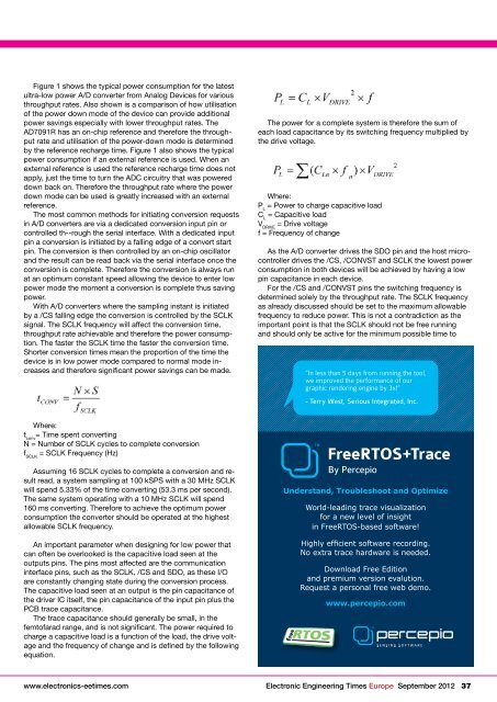
The power for a complete system is therefore the sum of<br />
each load capacitance by its switching frequency multiplied by<br />
the drive voltage.<br />
Where:<br />
P L<br />
= Power to charge capacitive load<br />
C L<br />
= Capacitive load<br />
V DRIVE<br />
= Drive voltage<br />
f = Frequency of change<br />
As the A/D converter drives the SDO pin and the host microcontroller<br />
drives the /CS, /CONVST and SCLK the lowest power<br />
consumption in both devices will be achieved by having a low<br />
pin capacitance in each device.<br />
For the /CS and /CONVST pins the switching frequency is<br />
determined solely by the throughput rate. The SCLK frequency<br />
as already discussed should be set to the maximum allowable<br />
frequency to reduce power. This is not a contradiction as the<br />
important point is that the SCLK should not be free running<br />
and should only be active for the minimum possible time to<br />
“In less than 5 days from running the tool,<br />
we improved the performance of our<br />
graphic rendering engine by 3x!”<br />
- Terry West, Serious Integrated, Inc.<br />
Where:<br />
t conv<br />
= Time spent converting<br />
N = Number of SCLK cycles to complete conversion<br />
f SCLK<br />
= SCLK Frequency (Hz)<br />
Assuming 16 SCLK cycles to complete a conversion and result<br />
read, a system sampling at 100 kSPS with a 30 MHz SCLK<br />
will spend 5.33% of the time converting (53.3 ms per second).<br />
The same system operating with a 10 MHz SCLK will spend<br />
160 ms converting. Therefore to achieve the optimum power<br />
consumption the converter should be operated at the highest<br />
allowable SCLK frequency.<br />
An important parameter when designing for low power that<br />
can often be overlooked is the capacitive load seen at the<br />
outputs pins. The pins most affected are the communication<br />
interface pins, such as the SCLK, /CS and SDO, as these I/O<br />
are constantly changing state during the conversion process.<br />
The capacitive load seen at an output is the pin capacitance of<br />
the driver IC itself, the pin capacitance of the input pin plus the<br />
PCB trace capacitance.<br />
The trace capacitance should generally be small, in the<br />
femtofarad range, and is not significant. The power required to<br />
charge a capacitive load is a function of the load, the drive voltage<br />
and the frequency of change and is defined by the following<br />
equation.<br />
Understand, Troubleshoot and Optimize<br />
World-leading trace visualization<br />
for a new level of insight<br />
in FreeRTOS-based software!<br />
Highly efficient software recording.<br />
No extra trace hardware is needed.<br />
Download Free Edition<br />
and premium version evalution.<br />
Request a personal free web demo.<br />
www.percepio.com<br />
www.electronics-eetimes.com Electronic Engineering <strong>Times</strong> <strong>Europe</strong> September 2012 37


