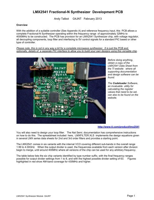
LMX2541 Fractional-N Synthesizer Development PCB - G4JNT
LMX2541 Fractional-N Synthesizer Development PCB - G4JNT
LMX2541 Fractional-N Synthesizer Development PCB - G4JNT

You also want an ePaper? Increase the reach of your titles
YUMPU automatically turns print PDFs into web optimized ePapers that Google loves.
<strong>LMX2541</strong> <strong>Fractional</strong>-N <strong>Synthesizer</strong> <strong>Development</strong> <strong>PCB</strong><br />
Andy Talbot <strong>G4JNT</strong> February 2013<br />
Overview<br />
With the addition of a suitable controller (See Appendix A) and reference frequency input, this <strong>PCB</strong> allows a<br />
complete <strong>Fractional</strong>-N <strong>Synthesizer</strong> operating within the frequency range of approximately 32MHz to<br />
4000MHz to be constructed. The <strong>PCB</strong> has provision for an <strong>LMX2541</strong> <strong>Synthesizer</strong> chip, with voltage regulator,<br />
all decoupling components, loop filter and interfacing to 5V control signals for a standard PIC based or other<br />
type of controller.<br />
Please note, this is not in any way a kit for a complete microwave synthesizer. It is just the <strong>PCB</strong> and,<br />
optionally, details of a separate PIC interface to allow you to build your own designs using this versatile chip.<br />
Before doing anything,<br />
obtain a copy of the<br />
<strong>LMX2541</strong> Data Sheet from<br />
the TI website where all<br />
supporting documentation<br />
and design software can be<br />
found.<br />
The Codeloader Software,<br />
an invaluable utility for<br />
calculating the register<br />
values that need to be set,<br />
can also to be found on the<br />
website.<br />
http://www.ti.com/product/lmx2541<br />
You will also need to design your loop filter. The Nat Semi. documentation has comprehensive instructions<br />
on how to do this. The spreadsheet included here, LMXFILTER.XLS implements the design equations given<br />
in several LMX series data sheets for 2nd and 3rd order filters and provides a starting point.<br />
The <strong>LMX2541</strong> comes in six variants with the internal VCO covering different sub-bands in the overall range<br />
1.99 to 4.00GHz When the output divider is used, the frequencies available from each version after division<br />
begin to merge, until around 400MHz where all versions of the chip can be used for any arbitrary frequency.<br />
The table below lists the six chip variants identified by type number suffix, with the final frequency ranges<br />
possible for output divider settings from 1 to 8, and with the highest possible divider setting of 63. Figures<br />
highlighted in red show AM-band coverage for 430MHz and higher.<br />
<strong>LMX2541</strong> <strong>Synthesizer</strong> Module <strong>G4JNT</strong> Page 1
Version VCO /<br />
1 2 3 4 5 6 7 8 63<br />
Q2060 1990 995.0 663.3 497.5 398.0 331.7 284.3 248.8 31.6<br />
2240 1120.0 746.7 560.0 448.0 373.3 320.0 280.0 35.6<br />
Q2380 2200 1100.0 733.3 550.0 440.0 366.7 314.3 275.0 34.9<br />
2530 1265.0 843.3 632.5 506.0 421.7 361.4 316.3 40.2<br />
Q2690 2490 1245.0 830.0 622.5 498.0 415.0 355.7 311.3 39.5<br />
2865 1432.5 955.0 716.3 573.0 477.5 409.3 358.1 45.5<br />
Q3030 2810 1405.0 936.7 702.5 562.0 468.3 401.4 351.3 44.6<br />
3230 1615.0 1076.7 807.5 646.0 538.3 461.4 403.8 51.3<br />
Q3320 3130 1565.0 1043.3 782.5 626.0 521.7 447.1 391.3 49.7<br />
3600 1800.0 1200.0 900.0 720.0 600.0 514.3 450.0 57.1<br />
Q3740 3480 1740.0 1160.0 870.0 696.0 580.0 497.1 435.0 55.2<br />
4000 2000.0 1333.3 1000.0 800.0 666.7 571.4 500.0 63.5<br />
Circuit Operation<br />
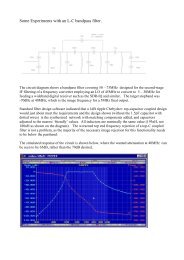
The circuit diagram is shown in Figure 1. A higher resolution version of the circuit diagram is stored as<br />
lmx2541y.gif. The reference signal is ideally supplied from an external master oscillator or low phase noise<br />
clock generator. Reference input level is not critical, and the data sheets suggests -40dBm as a lower limit;<br />
the maximum should not exceed 3.3V peak. The 51Ω termination resistor, R3 can be increased if loading is<br />
too high for a TCXO. Use any value you feel comfortable with, or leave it out altogether<br />
The charge pump output is filtered in C1, C2 and R2 . Programmable on- chip components allow for up to a<br />
fourth order filter – see the data sheet for more details’<br />
<strong>PCB</strong> Construction<br />
The <strong>PCB</strong> layout is shown in Figure 2, component references should tie-in with those in Figure 1. Component<br />
values not shown will depend on the design frequency and the PLL filter. Coupling and decoupling capacitors<br />
around the chip are 100nF – decoupling for high frequencies is internal to the chip Other decoupling ,<br />
including those for internal regulators should use the values shown.<br />
The only component that may give any difficulty in installation is the LM2541 itself. This should be fitted first,<br />
before any other components are added. The chip has 0.5mm pad spacing and is of the type where the<br />
connections are on the edge of the ceramic package, with no gull-wing tabs. The package is rectangular, with<br />
three pads each top and bottom, and nine on each side. A marker shows Pin 1 at the top left.<br />
This is how I solder the <strong>LMX2541</strong> device. Use a decent high magnification viewer; at least a headband type<br />
or for even greater magnification an old 50mm SLR camera lens is ideal. The pads on the <strong>PCB</strong> for the chip<br />
should first be tinned, aiming to keep an equal thickness of solder on each pad as shown in Photo 1. Then<br />
the pads should be liberally coated with flux. Double, triple and quadruple check k the IC alignment, place it<br />
central over the footprint so an equal amount of pad is showing on each side. Make sure there is flux still<br />
there on each pad. Press the IC down firmly, checking again for alignment. Peer though a magnifier at the IC<br />
pads sitting over the correct pads on the <strong>PCB</strong> while still pressing down on the IC. Look away for a few<br />
seconds to relax your eyes, return and check alignment again.<br />
Once absolutely certain each IC connection is above its pad, and unmoved, and still keeping it pressed down,<br />
using a medium-sized (typically 1mm) chisel-end soldering-iron bit place it in turn on each pad close to the IC,<br />
while watching the solder melt under the IC connections. The flux will cause a sort-of wicking action, drawing<br />
molten solder up from the pre-tinning to fill the gap to fix at least some of IC connections. Gently prod the<br />
chip to make sure it is now fixed by at least some pads and won’t move of its own accord. Now apply more<br />
flux to the IC / <strong>PCB</strong> and load the soldering iron tip with solder. Wipe the iron against each side of the chip in<br />
turn, gently pushing solder into the gaps. Providing there is enough flux present, it should nicely flow into the<br />
<strong>LMX2541</strong> <strong>Synthesizer</strong> Module <strong>G4JNT</strong> Page 2
minute gaps between each IC connection and its <strong>PCB</strong> pad. The flux – somehow, if there’s enough of it –<br />
always seems to prevent unwanted bridges forming. These are more likely if there is not enough flux, or the<br />
solder on the bit has been allowed to get dirty and oxidised.<br />
Once the chip appears to be fitted, breath a sigh of relief and get out the high gain magnifier. Look carefully at<br />
each joint making sure there is a continuous solder flow from <strong>PCB</strong> pad to IC connection. And also that there<br />
are no bridges. Bridges can be removed using solder wick / braid, again making use of extra flux at all times<br />
to aid solder flow and cleaning.<br />
When all the pads are soldered, the next stage is soldering the grounding pad on the underside. It is<br />
important that the IC has no chance of moving should the whole chip end up at solder melting point (which<br />
won’t harm it, provided this temperature is not sustained for more than a second or two). The best way to<br />
ensure it doesn’t move is to gently clamp the <strong>PCB</strong> upside down onto a non heat conducting surface. Paper<br />
clips holding the <strong>PCB</strong> onto a piece of cardboard or thin plywood works well. This ensures the IC is kept<br />
pressed onto its pads while the underside is soldered. Dd not apply too much force so the <strong>PCB</strong> bends! Apply<br />
more flux to the underside, running it into the plated through holes. Use a larger soldering iron bit, as quickly<br />
as possible apply solder until it flows though and is sucked down the 9 holes on the underside. When molten<br />
solder appears in a majority of holes stop heating and applying solder, and that should be it.<br />
If you have the right sort of a diode tester facility on a DVM, the connections to each pad of the IC can now be<br />
verified. The tester must have a voltage on the probes of no more than 2 – 3V open circuit, and no more than<br />
a couple of 100µA test current. If it meets these criteria connect the negative lead to ground and probe each<br />
IC connection in turn. All will show a voltage of between 0.7 to 1.8V. Any that Indicate the full Open circuit<br />
voltage are almost certainly not connected. I can’t vouch this test will work for other chips or different<br />
manufacturer’s products, but it does for this one. The tester must be a diode / continuity test with a constant<br />
current / voltage reading. Using the ohms range is not nearly so helpful.<br />
After fitting the main chip, installing the rest of the components should be straightforward!<br />
Apart from the large electrolytics around the LM1117, the majority of components can be of 0805 or 0603 size.<br />
The pads for C12 to C16 and C19 are a bit tight for 0805 components, but these can be squeezed on with<br />
care. The inductors can be 1206 size<br />
The <strong>PCB</strong> has been sized to fit inside a standard 37mm tinplate box, with the RF output provided by a socket<br />
soldered to the side in the conventional way for hard-cabled RF solutions.<br />
All power supply and signal pins are provided with through board connections, so these can be made on either<br />
side.<br />
Components List<br />
Quantity Reference Part<br />
1 IC1 LM1117 ‐ 3.3<br />
1 IC2 <strong>LMX2541</strong> (choose frequency variant)<br />
2 R3,R4 51 or higher to suit reference<br />
2 R9,R8 4k7<br />
3 R12,R10,R11 1k6<br />
3 R13,R14,R15 3k3<br />
1 C18 22u Rated for V IN maximum<br />
1 C17 47u > 6V wkg.<br />
3 R5,R6,R7 4.7<br />
2 C3,C9 1u<br />
1 C11 4u7<br />
8 C4,C7,C10,C12<br />
C13,C14,C15,C16<br />
100nF<br />
4 C5,C6,C8,C19 Typ. 470pF– 10nF to suit Freq.<br />
7 L1 to L7 Typ. 1u to 10uH<br />
3 C1, C2, R2 Loop Filter, custom values<br />
[1] R1 FastLock (if used)<br />
<strong>LMX2541</strong> <strong>Synthesizer</strong> Module <strong>G4JNT</strong> Page 3
Power Supplies<br />
The <strong>Synthesizer</strong> chip needs 3.3 V DD supplied by the on-board regulator; current consumption is<br />
approximately 100mA. Input voltage, V IN , can range from 4.5 to 20V. A heatsink is not necessary on the<br />
regulator for input voltages in the lower range.<br />
Resistors R10 – R15 allow the chip to be controlled with 5V logic levels. This allows a PIC to be used with a<br />
V DD suitable for allowing in-circuit programming. Vin to the regulator can be conveniently made equal to this<br />
5V, which is then supplied as one from a second external regulator.<br />
Programming and Getting it Going<br />
The chip’s internal registers have to be programmed to the correct values for your desired frequency and<br />
fractional grid, and the loop gain set, and etc etc etc . The data sheet and an understanding of <strong>Fractional</strong>-N<br />
synthesizers is essential here, but the easiest way to start off is to use National’s CodeLoader software to<br />
work out the values for you. This can be downloaded from the website shown above.<br />
CodeLoader shows a graphical representation of the RF PLL where you can interactively set frequencies and<br />
division ratios, as well as all the other PLL settings.<br />
.<br />
Also select whatever you want from the TP test point on pin 20. Setting this to deliver the divided down N or R<br />
dividers is instructive - it actually supplies a square wave at half the divided down or reference value and can<br />
make a quick confidence check of correct register programming before a complete closed loop system is<br />
established.<br />
Look at the waveform from here on a scope and experiment with programming the R3 register to toggle<br />
between divided down R and N values.<br />
Otherwise, the default registers programmed into the PIC will work as a starting point, but read the data sheet<br />
before modifying registers at will. For most operations, only R0, R1 and R2 need to be set to give a particular<br />
frequency, grid and reference. The other registers can be left alone.<br />
The <strong>LMX2541</strong>_PROG.EXE programme include in the archive allows quick calculation of the registers for<br />
specified values of Fosc, Fout and frequency tuning grid. It can be used in conjunction with a PIC containing<br />
the <strong>LMX2541</strong>CTL operating system as described in the appendix.<br />
PLL Filter Design<br />
The design of PLL filters for <strong>Fractional</strong>-N synthesizers is no different in concept from that for Integer-N<br />
designs, apart from the fact that the reference frequency is usually (a lot) higher with corresponding reduction<br />
in the integer part of N, and usually a higher loop bandwidth. The spreadsheet LMXFILTER.XLS (included<br />
in http://www.g4jnt.com/lmx2541Support.zip ) as shown in Figure 3 lets the basic values for the three<br />
main components forming the first two poles and the optional RC pair for a third pole be calculated. Enter<br />
values the figures highlighted in blue.<br />
The TI website also has loop filter design utilities http://www.ti.com/tool/clockdesigntool<br />
R1 provides for Fastlock operation if desired. See the data sheet for how this is implemented. For most<br />
applications it can be left out.<br />
<strong>LMX2541</strong> <strong>Synthesizer</strong> Module <strong>G4JNT</strong> Page 4
As an example, and to get going quickly, try these values for a starting point:<br />
K VCO<br />
30MHz/V<br />
BW 30kHz<br />
F REF 10MHz (= F COMP )<br />
R 1<br />
I CP<br />
1mA (Mid-Range)<br />
C1<br />
C2<br />
R2<br />
R1<br />
680pF<br />
15nF<br />
1k6<br />
Fastlock, Not installed<br />
VCO Tuning Sensitivity, K VCO , extracted from Data Sheet<br />
2060E 13 – 23 MHz / V<br />
2380E 16 - 30<br />
2690E 17 - 32<br />
3030E 20 - 37<br />
3320E 21 - 37<br />
3740E 24 – 42<br />
The lower number in the range applies when the VCO is at its<br />
lowest frequency and the higher number applies when the VCO is<br />
at its highest frequency. A linear approximation can be used for<br />
frequencies between these two cases.<br />
Contents of <strong>LMX2541</strong>Support.zip<br />
<strong>LMX2541</strong>_PROG.EXE (Register values, and control via RS232 / PIC O/S)<br />
<strong>LMX2541</strong>CTL.ASM(PIC firmware for RS232 control)<br />
<strong>LMX2541</strong>CTL .HEX “ “ “<br />
LMXFILTER.XLS<br />
<strong>LMX2541</strong>Y.gif<br />
(Higher resolution circuit diagram)<br />
<strong>LMX2541</strong>_Built.jpg<br />
<strong>LMX2541</strong> <strong>Synthesizer</strong> Module <strong>G4JNT</strong> Page 5
<strong>LMX2541</strong> <strong>Synthesizer</strong> Module <strong>G4JNT</strong> Page 6
`<br />
Fig 2<br />
<strong>PCB</strong> Component Placing<br />
Figure 4 Screen capture from the PLL Filter design spreadsheet<br />
File - LMXFILTER.XLS<br />
<strong>LMX2541</strong> <strong>Synthesizer</strong> Module <strong>G4JNT</strong> Page 7
Appendix A<br />
<strong>LMX2541</strong>CTL and <strong>LMX2541</strong>CTL_Delayed PIC Operating System<br />
A 12F629 PIC containing the <strong>LMX2541</strong>CTL code generates SPI data to allow the registers in the synthesizer<br />
chip to be set directly to the wanted values using a serial RS232, or COM Port interface with simple ASCII text<br />
commands from any terminal emulator programme such as Hyperterm. The register values can be<br />
programmed into non-volatile EEPROM memory in the PIC. At turn on, these stored values are recalled and<br />
sent to the synthesizer for immediate start up.<br />
The <strong>LMX2541</strong>CTL _Delayed version of the PIC firmware includes a three second delay after powering up<br />
before commands are sent to the synthesiser chip. This allows time for the reference input to the synth to<br />
become established. The boot up sequence involves some internal shenanigans within the chip where it uses<br />
the reference signal to for calibration of the VCO tuning range. If the reference is not present when the<br />
bootup process starts, PLL lock may not be established.<br />
Connect the RS232 lead and SPI connections as shown in Figure A1. The 4.7k resistor on the RS232<br />
interface serves to limit the current driven into the PIC input pin from the typical +/-9V of most RS232<br />
interfaces. Set the RS232 settings to 9600 baud, 8 bits, 2 stop bits, no parity, 9600-N-8-2. Flow control<br />
should be OFF. Turn on or reset the processor module, whereupon a display should appear, similar to that<br />
shown below. This shows a summary of allowed commands, followed by the stored register contents in both<br />
binary and hex that are immediately loaded into the chip. Note that characters typed are not echoed back;<br />
only responses will appear. If you want to see typed characters, set Local Echo ON in your terminal software.<br />
Registers are updated one at a time by typing R followed by eight digit hexadecimal representation of their<br />
new contents, terminated with a [cr].<br />
Example:<br />
R16880AC0[cr]<br />
(Note that the 0x shown on the response must not be typed).<br />
Followed by W [cr] to complete the actual EE write process.<br />
<strong>LMX2541</strong> CTRL<br />
Rxxxxxxx<br />
W<br />
INIT<br />
TEST<br />
0000 0000 0000 0000 0000 0000 0001 0111 0x00 00 00 17<br />
0000 0000 0000 0000 0000 0000 1100 1101 0x00 00 00 CD<br />
0000 0000 0000 0000 0000 0000 0001 1100 0x00 00 00 1C<br />
0010 1000 0000 0000 0001 0100 0000 1001 0x28 00 14 09<br />
0000 0001 0001 0001 1100 1110 0101 1000 0x01 11 CE 58<br />
0000 0000 0001 1110 0111 0010 1110 0110 0x00 1E 72 E6<br />
1010 0000 0000 0100 0000 0000 0000 0101 0xA0 04 00 05<br />
1111 1111 0100 1000 1000 0000 1010 0100 0xFF 48 80 A4<br />
0000 0000 1010 1100 0111 0011 0000 0011 0x00 AC 73 03<br />
0000 0110 0110 0010 0101 1010 0000 0010 0x06 62 5A 02<br />
0000 1001 0100 0000 0000 0000 0001 0001 0x09 40 00 11<br />
0001 0110 1000 1000 0000 1010 1100 0000 0x16 88 0A C0<br />
0001 0110 1000 1000 0000 1011 1100 0000 0x16 88 0B C0<br />
0x16 88 0B C0 Written<br />
The final LS digit of the eight defines<br />
the register address. See the data<br />
sheet for full details of register<br />
addressing. The new value is<br />
immediately transmitted to the<br />
synthesizer chip, which should<br />
respond accordingly.<br />
To save this new register value to<br />
non-volatile memory in the PIC, type<br />
W[cr] after the register contents have<br />
been accepted. A response will<br />
show that individual register has<br />
been written to EEPROM.<br />
To store multiple registers , enter<br />
these one at a time, issuing a W<br />
command for each. This is not as<br />
tedious as it sounds as subsequent<br />
updates will quite likely only require<br />
that one or two registers be altered<br />
at a time.<br />
If you get in a mess, type INIT[cr] which has the same effect as switching off and back on, reloading all the<br />
registers with the prestored values. When updating the EEPROM with several new values, it is worth issuing<br />
INIT commands periodically to check these have all been stored correctly.<br />
<strong>LMX2541</strong> <strong>Synthesizer</strong> Module <strong>G4JNT</strong> Page 8
The <strong>LMX2541</strong>_Prog Software (Figure A2) can send the ASCII text automatically to the controller, To enable<br />
this option, simply set the value in the COM Port window shown in red.<br />
Figure A1 PIC Interface for <strong>LMX2541</strong>CTL Operating System<br />
Fig A2 <strong>LMX2541</strong>_Prog<br />
User Screen<br />
<strong>LMX2541</strong> <strong>Synthesizer</strong> Module <strong>G4JNT</strong> Page 9