VHF Synth Module - G4JNT
VHF Synth Module - G4JNT
VHF Synth Module - G4JNT
- No tags were found...

Create successful ePaper yourself
Turn your PDF publications into a flip-book with our unique Google optimized e-Paper software.
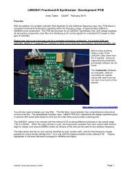
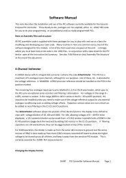
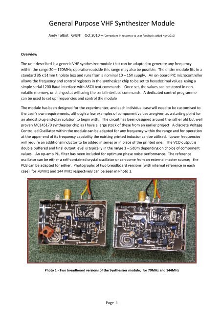
General Purpose <strong>VHF</strong> <strong>Synth</strong>esizer <strong>Module</strong>Andy Talbot <strong>G4JNT</strong> Oct 2010 – (Corrections in response to user feedback added Nov 2010)OverviewThe unit described is a generic <strong>VHF</strong> synthesizer module that can be adapted to generate any frequencywithin the range 20 – 170MHz; operation outside this range may also be possible. The entire module fits in astandard 35 x 51mm tinplate box and runs from a nominal 10 – 15V supply. An on-board PIC microcontrollerallows the frequency and control registers in the synthesizer chip to be set to hexadecimal values using asimple serial 1200 Baud interface with ASCII text commands. Once set, the values can be stored in nonvolatilememory, or changed at will using the serial interface commands. A dedicated control programmecan be used to set up frequencies and control the moduleThe module has been designed for the experimenter, and each individual case will need to be customised tothe user’s own requirements, although a few examples of component values are given as a starting point foran almost plug-and-play solution to begin with. The circuit has been designed around the rather old but wellproven MC145170 synthesizer chip as I have a large stock of these from an earlier project. A discrete VoltageControlled Oscillator within the module can be adapted for any frequency within the range and for operationat the upper end of its frequency capability the existing printed inductor can be utilised. Lower frequencieswill require an additional inductor to be added in series or in place of the printed one. The VCO output isdouble buffered and final output level is typically in the range 1 – 5dBm depending on choice of componentvalues. An op-amp PLL filter has been included for optimum phase noise performance. The referenceoscillator can be either a self-contained crystal oscillator or can come from an external master source; thePCB can be adapted for either. Photographs of two breadboard versions (with internal reference in eachcase) for 70MHz and 144 MHz respectively can be seen in Photo 1.Photo 1 - Two breadboard versions of the <strong>Synth</strong>esizer module; for 70MHz and 144MHzPage 1
Figure 1 Circuit Diagram of the Complete <strong>Synth</strong>esizer <strong>Module</strong>Page 2
Circuit DescriptionThe complete circuit diagram is shown in Figure 1, with component values shown where they do not have tobe selected for any particular frequency range. The Colpitts VCO based around a UHF bipolar has its outputlightly coupled to a second bipolar buffer followed by a MAR-2 modamp to raise the output to a useful level.A portion of the final RF is tapped off to feed the MC145170 synthesizer device. Dual back-to-back tuningdiodes are used in the VCO to optimise the Q and hence improve phase noise.There is provision on the PCB for either a crystal oscillator – which is part of the MC145170 chip – or anexternal reference by fitting the components appropriate in each case. Connections for either are shown bydotted lines. A trimmer for adjusting the internal reference can be installed using the pad / hole on the PCBthat alternatively serves as the connection for an external referenceThe two Ø V and Ø R outputs from the PLL’s phase detector are taken to an op-amp filter whose componentvalues can be determined either from the spreadsheet at [1] or from any standard PLL design literature. Anextra filter element is available by choice of suitable values for the RC network between the op-amp outputand the tuning diodes. The op-amp type is not shown on the diagram. An NE5532 was used for thebreadboards, but most low noise types will be acceptable. The PCB layout is designed around using one sideof a dual op-amp device with standard connections.An integral 5V regulator supplies the PIC and synthesizer, and this stabilised supply is also used for the VCOand first buffer. Extensive decoupling using chip inductors is applied on each power supply delivery point.The unregulated input voltage is used for biasing the MAR-2 output amplifier and as supply to the op-ampfilter. This allows the VCO tuning voltage to swing over the range typically 2 – 10V .Some component values to start with around the VCO can be found in Appendix 1 .PLL Design information is in Appendix 2PCB LayoutThe double sided PCB is designed to fit into a standard 37 x 55 x 30mm tinplate box such as Type No1000112 available from G3NYK [2]. The component overlay can be seen in Figure 2 All components aresurface mounted, with the majority of R and C being of 0805 size. Decoupling inductors are 0812dimensions but there is enough leeway in pad sizes to allow other device outlines to be squeezed in. All ICsapart from the 78L05 voltage regulator are of the 1.27mm pin spacing SOIC type.The lower side is a continuous groundplane. Pads shown as circular on the layout are connections to ground– use links on home produced PCBs. Spare pads are for connections through, and must be counterbored onthe groundplane side to prevent short circuits.A Mirrored .PDF file of the PCB at 2X scale can be found at [3]Page 3
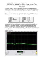
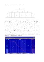
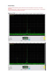
Figure 2 PCB OverlayPerformanceMeasured phase noise can be seen in Figure 3 and Figure 4 respectively for the 144 and 70MHz breadboardmodules. The high band unit has been programmed for a comparison frequency of 50kHz with a loopbandwidth of 5kHz. The resulting spurious of the sideband can be seen in the second photo of Figure 2 at alevel of -62dBc. The low band module was set at an obscure comparison frequency around 16kHz in orderto generate a precise output, and its resulting sidebands are at a very acceptable -78dBc. Loop bandwidthfor this configuration was around 2kHzPage 4
Figure 3 Measured Spurious and Phase Noise of the 144MHz UnitPage 5
Figure 4 Spurious and Phase Noise at 70MHzIn each case resolution bandwidth is 3Hz, so the dBc/Hz value can be determined by adding 5dB to the valueread off at any particular offset from the curves. At 144MHz, for example, at 60kHz separation from thecarrier phase noise can be seen to be at a level of around -120dBc/Hz.ProgrammingThe 8 pin 16F629 PIC device has three of its connections made available to pads on the PCB. The device isconfigured for in-circuit programming to load in new firmware. Any PIC programmer such as the PicKit fromMicrochip can be connected to the PGC/PGD/PGM (Programming Clock, Data and Program) pins for chipprogramming.The PGC and PGD pads also serve as direct connection to a serial RS232 interface for controlling the chip overa 1200 baud serial interface using ASCII text based commands to send hexadecimal data for setting theregister contents. These can be taken out through feed-through capacitors, but two external resistors arerequired. A 4.7kΩ resistor is needed in series with the serial data input from the PC to prevent possible chipdamage from over current on its negative voltage excursions. On the data output to the PC, a 330Ω resistorwas needed to allow in-circuit programming. If not present, the capacitance of the feed-through wassufficient to load the programmer connected directly to the pads on the PCB and prevent it from functioning.The resistor allowed adequate isolation to let the high speed programming information past.A simple operating system is included on the PIC (in firmware named MC145170ctl.asm) that allowsinteractive setting of the registers using a terminal programme such as Hypertrm set to 1200 baud, 8 bit data,no parity, 1 stop bit. If the terminal / serial interface is connected when power is applied to the controller,the introductory message shown in the Hyperterminal screenshot below will be seen. Once connection isestablished, commands available for setting each of the three R, N and C registers within the MC145170 canbe issued. These are :Page 6
Rxxxx, Nxxxx, Cxx, U and W.In each case the command is terminated with a [rtn]xxxx are hexadecimal characters and exactly the number shown (four or two) must be entered. They can bein upper or lower case. To see how the 8 bits (two hex characters) that make up the C command for settingthe control register as configured see the data sheet, but for most practical purposes on this module the hexvalue of 33 will be suitable. This value should have been programmed into the PIC’s non-volatile memoryinitially so there should be no need to change this unless desired.For example, using a reference oscillator of 4MHz, 50kHz comparison frequency and a wanted output of145.35MHz first calculate the hex values needed:R = 4MHz / 50kHz = 80 (in decimal). Convert to 4 character Hex = 0050N = 145.35MHz / 50kHz = 2907 decimal Convert to Hex = 0B5BThen type in the following commands in turn: R0050 [rtn], N0B5B [rtn] ( C33 [rtn] optional)A screenshot from Hypertrm is illustrated in Figure 5 below.In each case the terminalwill echo back the valueentered if accepted. If noreply is seen, thecommand may have beentry again until theresponse is seen.R / N / C commands canbe entered in any order.At this point the outputfrequency will not yethave changed.Figure 5Once both R and N (andpossibly C) registers havebeen set, then typeU [rtn] which is thecommand to update theMC145170 chip itself.To save the values permanently to EE memory, issue a W [rtn] command to write all three values to nonvolatilememory as well as updating the chip. When accepted, the values will again be echoed back to thescreen – although note that the U or W will not be shown.Page 7
Programming UtilityA stand-alone utility for setting frequencies directly can be found at [4] with screenshots from this illustratedin Figure 6.At start up, the window will appear as shown on the left. The three red boxes must first be filled in with thereference frequency, the wanted output and the COM port to be used for communication with the module.A comparison frequency can be selected from the pull down menu, or any obscure value can be typed ininstead. The individual C register functions and flags can be set by ticking or clearing the appropriate boxes– for most purposes leave these at the defaults. Then, when all the values have been entered, click the twoor three buttons, Set R , Set N and Set C which send each of the three commands to the module in turn.The response in each case will appear in the lower right window. When complete, click the Update orWriteEE buttons.Figure 2 Opening and operational screenshots of the MC145170 Programming Utility--------------------------------------------------------------------------------------------------------------------------------------------References[1] PLL Design Spreadsheet PLL.XLS[2] G3NYK http://www.alan.melia.btinternet.co.uk/componen.htm[3] PCB Copper at 2* mirrored <strong>VHF</strong><strong>Synth</strong><strong>Module</strong>_PCB_TopCopper_X2_Mirrored.pdf[4] Programming Utility 145170Ctl.EXE (rename from .EEX)Files can be found inwww.g4jnt.com/<strong>VHF</strong><strong>Synth</strong><strong>Module</strong>.zipPage 8
Appendix 1Some component values to start with.Varicap type BB149 was used here. This gives a capacitance of approximately 15 to 5pF for 2 – 10VQ2 / Q3 need to be SOT-23 packaged RF transistors providing adequate gain at the frequency of interest.UHF devices such as BFR92 are eminently suitable for upper <strong>VHF</strong> use. Or almost any other UHF type.C33 was a 20pF preset for breadboarding purposes. In a finished design this should preferably be replacedby a fixed value. A core-adjustable inductor was used for the low band version.The printed inductor has approximately 140nH inductance.Component High Band 145MHz Low Band 70MHzTuning Inductor Full printed ~ 140nH Cut printed inductorand add additional200nH in seriesC22 4.7pF 6.8pFC4 47pF 68pFC5 22pF 33pFC7 4.7pF 10pFR9/C16 1k / 33nF 1.3k / 33nFTuning Sensitivity 1.5MHz/Volt 0.9MHz/VoltComparison Freq 50kHz 25kHzPage 9
Appendix 2PLL DesignR6 / R7 =R5 / R8 =C14 / C20R9C168k213k33nF1k33nFR6 / R7 =R5 / R8 =C14 / C2010k20k33nFR9 1.3kC1633nFPage 10