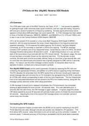
G4JNT 144MHz direct conversion receiver with I/Q outputs for use ...
G4JNT 144MHz direct conversion receiver with I/Q outputs for use ...
G4JNT 144MHz direct conversion receiver with I/Q outputs for use ...

Create successful ePaper yourself
Turn your PDF publications into a flip-book with our unique Google optimized e-Paper software.
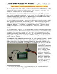
<strong>144MHz</strong> <strong>direct</strong> <strong>conversion</strong> <strong>receiver</strong> <strong>with</strong> I/Q<strong>outputs</strong> <strong>for</strong> <strong>use</strong> <strong>with</strong> Software Defined Radio.OverviewThis design is a <strong>direct</strong> <strong>conversion</strong> <strong>receiver</strong> <strong>for</strong> <strong>144MHz</strong> <strong>with</strong> quadrature <strong>outputs</strong> <strong>for</strong> <strong>use</strong> either <strong>with</strong> asoftware defined radio (Reference 1) or <strong>with</strong> additional audio phasing circuitry. Quadrature <strong>outputs</strong>,generated from two 90 degree shifted local oscillators, allow SSB reception by unwanted sidebandcancellation as described in Reference 2.The converter was designed <strong>with</strong> the primary aim of using it <strong>for</strong> the IF stage on microwave transverters, soa linear <strong>receiver</strong> was needed <strong>with</strong> no AGC, but a calibrated gain control to make accurate relativemeasurements of microwave beacons using a PC Soundcard based system <strong>for</strong> the actual level and Signal toNoise ration measurements. A straight<strong>for</strong>ward gain calibration can then be <strong>use</strong>d to convert these intoabsolute readings, making this a <strong>use</strong>ful piece of test equipment <strong>for</strong> propagation studies.There is nothing inherently narrowband in the design - filtering limits the RF bandwidth to around 8MHz toeliminate strong signals from broadcast and PMR, and audio bandwidth is kept to about 20kHz , wideenough <strong>for</strong> the normal maximum soundcard sampling rate of 44100Hz. Any subsequent audio filtering <strong>for</strong>actual listening purposes is per<strong>for</strong>med by the SDR software, or in separate audio processing circuitry.OperationThe circuit diagram is shown in Figure 1.In the RF path two modamps, a MAR-6 and a MAR-3 amplify the RF; there is a two stage bandpass filterbetween them <strong>with</strong> 10MHz bandwidth. The output feeds into two SRA-1 type DBMs via a resistivesplitter, <strong>with</strong> the quadrature LO signal generated using a MiniCircuits PSCQ-2-160. This deviceguarantees less than 3 degrees phase error over 100 to 160MHz; as <strong>144MHz</strong> is near the middle of the rangewe can expect a fair bit better per<strong>for</strong>mance here.The local oscillator is an AD9851 DDS, currently clocked at 100MHz, generating 16 to 16.67MHzfollowed by a X9 RF multiplier. The DDS source is not described here, but the module in a basic <strong>for</strong>m isdescribed in Reference 3. The active stages in the multiplier consist of MAR-6 modamps configured as apair of cascaded tuned X3 stages <strong>with</strong> a final MAR-6 as amplifier/limiter, this combination <strong>for</strong>mingprobably the simplest tuned RF multiplier possible! (There are a couple of CW spurii generated by theDDS, but I know where they are and can ignore them). All filtering is designed to allow the LO to tuneover 144 to 150MHz to cover a bit wider than the normal 2MHz narrowband segments on the microwavebands, and allow <strong>for</strong> odd LO frequencies. Multiplier output level is +10dBm drive to the quadraturehybrid.By using the internal X6 option in the AD9851 DDS Chip, the LO can be driven from a 10MHz frequencyreference, producing a clock of 60MHz, but this has not been implemented yet. Hopefully spurious levelswill be no worse, <strong>with</strong> none falling in the beacon bands at the lower clock frequency.The mixer <strong>outputs</strong> drive a pair of identical NE5532 opamps <strong>with</strong> a voltage gain approaching 300 (exactvalue a bit uncertain due to internal impedance of the mixer IF port) No clever matching, just the mixerfeeding the inverting input giving 800 ohms input resistance at audio, and low pass filtering to get rid of RFleakage. The I/Q <strong>outputs</strong> feed another pair of op-amps <strong>with</strong> precisely switchable gain from 0 to 40dB in10dB steps. Audio bandwidth is not especially tailored, but rolls off gently from about 20kHz to allow <strong>for</strong>44100Hz sampling rate in a soundcard.The total system gain and dynamic range is based on 16 bit digitisation, and is sufficient at maximum(+40dB) to place its own thermal noise least 10dB above the quantisation noise pedestal. Strong signals
and extra RF gain in transverters is catered <strong>for</strong> by backing off the audio gain. For signals too strong even<strong>for</strong> this (80db S/N in 20kHz) an external (calibrated) RF attenuator can be addedConstructionNo attempt was made to put this on a proper PCB. The converter and audio stages were built birds-neststyle on a piece of unetched copper clad PCB as can be seen in Photograph 1. Plenty of decoupling andshort <strong>direct</strong> wires ensure stable per<strong>for</strong>mance. As there is a lot of gain - particularly at audio - the wholeunit was built into a tinplate box <strong>for</strong> screeningUsing parallel and series 1% resistors <strong>for</strong> the switchable gain stage, no especial trimming or adjustment wasnecessary, the traces looked well enough matched on a 'scope and as I was only after 20 - 25dB sidebandrejection to make opposite sideband noise insignificant, tweaking wasn’t necessary. 3 degrees phase errorwill give 25dB rejection, assuming amplitude is correct, which is about equivalent to 5% amplitudeimbalance. So if I have a 'bit better' in each case the 20dB plus is easily achievable. All power rails areregulated and well filtered <strong>for</strong> operation off a portable 12V supply.The LO multiplier was made by cutting a 50 ohm microstrip line into a double sided PCB. To quicklymake a 50 ohm line <strong>with</strong>out etching, score two lines 2.8mm apart through the copper on the top face of thePCB <strong>for</strong> the full width, <strong>use</strong> a Stanley knife or similar making sure you penetrate the copper fully. 2.8mmwidth on normal 1.6mm thick fibreglass PBC gives about 50 ohms characteristic impedance. Then scoretwo more lines about 1mm from each of these. Using a hot soldering iron, <strong>use</strong> this to soften the adhesiveand <strong>with</strong> a pair of tweezers, lift up and remove the two 1mm wide strips, which will give a single 50 ohmline surrounded by copper groundplane. Drill a number of 0.8 to 1mm holes through the top ground planeto the underside and fit wire links to give a solid RF ground structure. Wire links are best fitted close towhere grounding and decoupling components are connected.Cut the 50 ohm line into segments <strong>with</strong> gaps <strong>for</strong> the modamps, DC blocking capacitors and filters. Otherconnections around the filters are made up birds nest style. When completed and aligned, coils can be heldin place <strong>with</strong> glue (a hot glue gun is a <strong>use</strong>ful accessory to have around) Photograph 2 shows thecompleted multiplier chain.Using the downconverter.For the standalone unit <strong>for</strong> <strong>use</strong> as a <strong>receiver</strong> in the field, a simple quadrature network and loudspeaker ampcan be added to make a complete <strong>receiver</strong>. A high/low pass pair of all pass networks will give 15dBsideband rejection over 400Hz to 2kHz which is good enough <strong>for</strong> listening to beacon signals on hill tops.Alternatively, look at Reference 2 <strong>for</strong> phasing type SSB networks to give an improved SSB per<strong>for</strong>mance.A meter driven from the audio level via a precision rectifier circuit can be added to allow quite precisesignal strength measurements to be made in conjunction <strong>with</strong> the calibrated attenuator. Alternatively, takeat look at the Software Defined Radio software (Ref 1) from I2PHD <strong>for</strong> another solutionLO SourceThe DDS module as described in Ref. 3 has new PIC software, along <strong>with</strong> a rotary encoder and LCDdisplay to give a <strong>use</strong>r friendly interface. For anyone who has the original DDS board I can supply PICsoftware <strong>for</strong> this modification. However, the AD9850 and ‘9851 chips are in short supply now - they havebeen replaced in most cases by larger, faster, new devices in a different package.Alternatively, emulate the venerable IC202 transceiver and build a VCXO to supply the signal to themultiplier. Or <strong>use</strong> a VFO/mixer, or a synthesizer - the choice is yours!
Ref 1 http://www.sdradio.orgRef 2 RadCom series on phasing networks Feb to June 2004.Ref 3 AD9850 DDS Module RadCom, November 2000Figure 1Photo 1Photo 2Circuit DiagramRF and Audio stages.Local Oscillator multiplier