Single Conversion LF Upconverter - G4JNT
Single Conversion LF Upconverter - G4JNT
Single Conversion LF Upconverter - G4JNT

You also want an ePaper? Increase the reach of your titles
YUMPU automatically turns print PDFs into web optimized ePapers that Google loves.
<strong>Single</strong> <strong>Conversion</strong> <strong>LF</strong> <strong>Upconverter</strong> Andy Talbot <strong>G4JNT</strong> Jan 2009Mark 2 Version Oct 2010,see Appendix, Page 8This upconverter is designed to directly translate the output from a soundcard from a PCrunning datamode software up to the final wanted transmission frequency. It is not necessarythat the software generates a stereo quadrature output as this can be done in hardware, but ifthe stereo option is available, improved performance with regard to spurious outputs ispossibleThe upconverter adopts a single conversion image reject topology, and has been designedwith reproducibility in mind – in particular there should be a minimum number of ‘tweaks’needed to get it going. Two mixers are driven by quadrature local oscillator signals, with theaudio input to each supplied with a 90 degree phase shift applied between them (I and Qchannels). When the outputs from the two mixers are subsequently added, one mixersideband is cancelled and the other reinforced.MixerInitially a circuit using a pair of NE612 mixers was tried [1a] , but it proved impossible toachieve a carrier rejection better than 30dB. Opposite sideband suppression requiredconsiderable effort with phase and amplitude trimming to achieve a barely acceptableperformance and this design was subsequently abandoned. A configuration using a pair of(now obsolete) MC1496 devices could achieve a more-than-adequate performance [1b] butthe circuit is complicated by the need for external bias resistors and trimming, so was alsorejected.The solution finally adopted was based around an FST3125 bus switch quadrature mixer, asused in a number of HF SDR front end designs such as the Softrock receiver [2] . Unlike thewell known Quadrature Sampling Detector (QSD) topology with its four successive 25% dutycycle pulses, a simple quadrature drive is adopted here which simplifies the drive circuitslightly and does not appear to detract from performance.The circuit can be seen in the right hand part of Figure 1 and should be reasonably selfexplanatory. All four phases (0/90/180/250 degrees) are obtained from a synchronouslyclocked pair of flip flops driven at four times the wanted clock frequency. The external clockinput has a buffer that allows an input of –10dBm or greater to properly clock the counter.Each phase drives one of four SPST bus switches.Two unity gain op-amp buffers have a high input and a low output impedance. Drive to themixer switches is through two 680 ohm resistors to essentially turn the drive into currentsources. Each of these two audio signals are switched alternately to opposite sides of abalanced output transformer at LO rate, offset by 90° phase shift between the two channels.Accurate balance of the output transformer determines the carrier suppression that can beachieved, and is probably the only critical component. The primary must be a bifilar wound foraccurate balance, and it is probably best if all three windings are wound in a trifilar fashiongiving a transmission line transformer. 20 trifilar turns on a small low frequency ferrite torroidof uncertain heritage proved satisfactory down to well below 100kHz. The bus switches are<strong>G4JNT</strong> Direct <strong>LF</strong> <strong>Upconverter</strong> Page 1
iased to 2.5V on input and output ports to maximise their linearity; a common divider suppliesall bias points.To complete the mixer a simple low pass filter reduces harmonics. The component valuesshown cut off at 530kHz - these will have to be altered for operation at other frequencies..IQ Source GenerationIf stereo I/Q outputs are available from the transmit software, the mixer as described is all thatis required to provide an image cancelling upconversion. All such software, for example thatin [3], provides fine trimming of amplitude and phase and when correctly set up can give over40dB of sideband rejection, over 50dB can sometimes be achieved with care.Where I/Q outputs are not available, as is the case with most current datamode software, the90° I/Q audio drives have to be generated in hardware. Many designs have appeared overthe years, some with quite complex configurations giving acceptable full speech-bandperformance. However, these were usually used in zero-IF configurations where theunwanted product lay on top of the wanted signal, so a sideband rejection of 20dB was oftenadequate. Here we are not using a zero IF, so opposite sideband rejection is critical toperformance.For <strong>LF</strong> use, we are only really interested in a narrow audio range for low bandwidthmodulations, and provided we restrict the audio to no more than a few hundred Hz in width, aremarkably accurate phase shift can be formed from a simple all-pass circuit configuration.The circuit on the left hand side of Figure 1 shows the all-pass network which has beenseparated from the mixer stage to allow each part of this converter to be used on its own. Seethe note at the end for further simplification. Two preset resistors allow the frequency rangeand suppression to be traded-off. To see the range of values that can be achieved, an Excelspreadsheet is provided [4] that allows rejection to be plotted over the audio band as the allpasscomponent values are altered.AlignmentIt helps greatly if a wideband spectrum display that can show both output sidebandssimultaneously, such as an SDR is used. Connect the converter output though anappropriate attenuator to the receiver input. If a wideband receiver is not available a normalSSB receiver can be used, either by tuning over the two sidebands, or by switching betweenLSB/USB reception.Apply an audio tone of the desired frequency, and observe both sidebands and carrier leakagewhich should be around the –40dB region. There is no scope for adjusting carrier leakage(balance). If this is significantly worse than 40dB, it suggests an imbalance in the outputtransformer or incorrect connections or a damaged bus-switch chip. There is little scope forany other mechanism to degrade carrier rejection.Ensure the correct sideband is selected; as shown the circuit is fixed for USB generation –swap I/Q channels to change to the other conversion direction. Adjust the two presets for thebest sideband rejection.<strong>G4JNT</strong> Direct <strong>LF</strong> <strong>Upconverter</strong> Page 2
ejection of –40dBc, which at <strong>LF</strong> will probably result in out of band signals, is considered to bean acceptable level of spurious products by many authorities.It is up to you to decide if this rejection figure is acceptable or not!References[1a] - http://www.g4jnt.com/IQConverters.htm Fig 3[1b] - “ “ “ “ “ FIg 1[2] - http://www.softrockradio.org/node/1[3] - G3PLX SDR transmitter softwarehttp://www.g4jnt.com/SDRTxSW.htm[4] - http://www.g4jnt.com/OPA_AllPass.xlsAlter the values of C1 R1 C2 R2 to see how the rejection vs. frequency responsealters.<strong>G4JNT</strong> Direct <strong>LF</strong> <strong>Upconverter</strong> Page 4
Figure 1 - Complete <strong>Upconverter</strong> circuit diagram<strong>G4JNT</strong> Direct <strong>LF</strong> <strong>Upconverter</strong> Page 5
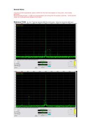
Figure 2 - AF Drive Broadband noise source + 1.5kHz toneAll-pass network optimised for 1.0kHz and 1.5kHzCentre Freq 502kHzFigure 3 Centre Freq 137kHz , adjusted all-pass network<strong>G4JNT</strong> Direct <strong>LF</strong> <strong>Upconverter</strong> Page 6
Figure 4 Sideband isolation at 1500Hz improved by fine adjustment ofamplitude balance. (No noise signal)Figure 5 - The finished thing!<strong>G4JNT</strong> Direct <strong>LF</strong> <strong>Upconverter</strong> Page 7
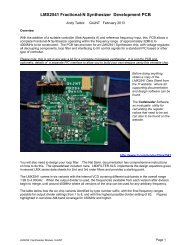
AppendixNew Improved version with Double Balanced Mixer Oct 2010After building the Mark 1 version, I then realised that by doing the mixer differently, it would bepossible to avoid the need for an accurately balanced output transformer. The opportunitywas also taken to make a proper PCB layout.The circuit shown in Figure A1. The analogue input circuitry is more-or-less the same as forthe original, but with the quadrature network integrated onto the board, and an I/Q input optionselectable by removing / shorting some of the components around the op-amp buffer.The mixer uses a dual quad bus switch to implement a quadrature double balanced mixer.Note that as the binary ring counter counts 0,1,3,2, or in binary 00, 01 11, 10, the pairs ofinput lines have to be swapped round to accommodate this.An improved RF input buffer was added, and an output amplifier raising the maximum outputto around +4dBm. The Low Pass filter cuts off at 530kHz.Results.The main improvement seen is in the area of carrier rejection. At full output, with an audiodrive of 1V RMS giving +4dBm out, a carrier rejection of 50dB can be achieved with no needfor an accurately wound output transformerSideband rejection is a function of the I/Q network, and remains similar to that for the original,although improved rejection can be obtained at a single frequency due to the better outputbalancing. 50dB rejection was seen at 1500Hz input by careful adjustment of the presets.Some photographs of the finished unit are shown below, along with the PCB overlay. Theunderside consists of a continuous groundplane layer, with through links on each of the roundpads. The square pads are not grounded, and need to be counterbored on the reverse if pinsare used for connections to them.<strong>G4JNT</strong> Direct <strong>LF</strong> <strong>Upconverter</strong> Page 8
Figure A1 Direct <strong>LF</strong> <strong>Upconverter</strong> Mark 2 - Double Balanced Mixer version<strong>G4JNT</strong> Direct <strong>LF</strong> <strong>Upconverter</strong> Page 9
<strong>LF</strong> <strong>Upconverter</strong> PCB mounted above the RF source( based around an AD9850 DDS chip.A 2:1 size mirrored image of the copper forhome construction of the PCB can be foundbelow. Contact <strong>G4JNT</strong> for PCB details inother formats<strong>G4JNT</strong> Direct <strong>LF</strong> <strong>Upconverter</strong> Page 10
<strong>G4JNT</strong> Direct <strong>LF</strong> <strong>Upconverter</strong> Page 11
<strong>G4JNT</strong> Direct <strong>LF</strong> <strong>Upconverter</strong> Page 12