Electronics Spectra - SMS Lucknow
Electronics Spectra - SMS Lucknow
Electronics Spectra - SMS Lucknow

Create successful ePaper yourself
Turn your PDF publications into a flip-book with our unique Google optimized e-Paper software.
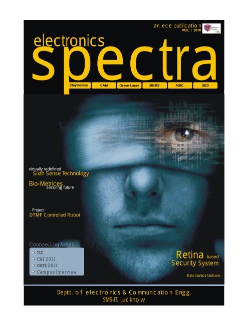
an ece publication<br />
VOL. I 2010<br />
spectra<br />
electronics<br />
Claytronics CAM Green Laser MEMS<br />
ASIC<br />
SED<br />
virtually redefined<br />
Sixth Sense Technology<br />
Bio-Metrices<br />
securing future<br />
Project<br />
DTMF Controlled Robot<br />
Counselling Arena<br />
IES<br />
CAT 2011<br />
GATE 2011<br />
Campus Interview<br />
Retina based<br />
Security System<br />
E lectronics Unborn<br />
Deptt. of electronics & Communication Engg.<br />
<strong>SMS</strong>-IT, <strong>Lucknow</strong>
DEPARTMENT OF<br />
ELECTRONICS & COMMUNICATION<br />
<strong>Electronics</strong> and Communication Engineering is one of the most upcoming area of Research & Engineering<br />
among all other branches of engineering. As of today, <strong>Electronics</strong> and Communication Engineers are<br />
working in all spheres of modern industry. The goal of this course is to impart all around technical education<br />
to the students to fulfill requirements of new challenges of industries as well as to find new ways to solve the<br />
practical problems of our daily life.<br />
The Department of <strong>Electronics</strong> and Communication Engineering was established in the year 2008 in <strong>SMS</strong><br />
INSTITUTE OF TECHNOLOGY, LUCKNOW. The department has well equipped Labs as :<br />
Electronic Workshop & PCB Lab<br />
<strong>Electronics</strong> circuit Lab<br />
Digital <strong>Electronics</strong> lab<br />
Measurement Lab<br />
Integrated Circuit Lab<br />
Advanced Communication lab<br />
Microprocessor Lab<br />
Control System Lab<br />
Micro-wave & Research Lab<br />
Design & Simulation Lab<br />
The department has prominent Faculty members having a vast experience in their field.<br />
Industrial visits and practical projects are also encouraged by the department in various sectors. Students<br />
are also taken out to industries for practical understanding of the new technologies. Recently we had an<br />
Industrial Tour to NEDA, <strong>Lucknow</strong> and a Seminar on Embedded Technology.
<strong>SMS</strong> Institute of Technology, L ucknow<br />
Department of <strong>Electronics</strong> & Co mmunication<br />
MESSAGE<br />
Dear Students,<br />
This gives me immense pleasure to say few words for the intellectual initiative<br />
taken by the students of <strong>Electronics</strong> & Communication Engineering, in bringing out<br />
the first issue of “<strong>Electronics</strong> <strong>Spectra</strong>”.<br />
I am confident that the initiative will not only bring laurels to the student community<br />
but will also open new vista for further innovations.<br />
Sustaining the professional impeccability of a new age “Technology Magazine” is a<br />
daunting challenge and we must be armed to face it.<br />
The passage of time will ensure the acceptability of the contributions of the writers.<br />
The critical feedback of the readers shall build a continuous improvement system that will lead the <strong>Electronics</strong><br />
<strong>Spectra</strong> towards excellence.<br />
Wishing <strong>Electronics</strong> <strong>Spectra</strong> a grand success in the future.<br />
With best wishes!!<br />
Sharad Singh<br />
Chief Executive Officer<br />
<strong>SMS</strong> Group of Institutions, <strong>Lucknow</strong><br />
I am pleased to know that the Department of <strong>Electronics</strong> & Communication Engineering<br />
of <strong>SMS</strong> Institute of Technology, <strong>Lucknow</strong> is bringing out its first issue of<br />
"<strong>Electronics</strong> <strong>Spectra</strong>" . I extend my best wishes on the occasion of the publication of the<br />
first issue of the technical magazine.<br />
I hope this magazine will be a treasure for those associated with <strong>Electronics</strong> &<br />
Communication Engineering and will help in providing a platform for sharing experiences<br />
& learning in this area.<br />
I once again congratulate the <strong>Electronics</strong> & Communication Engineering Department<br />
and the entire team on this endeavour and wish the Technical Magazine all success.<br />
Dr. G.D. Singh<br />
Director<br />
<strong>SMS</strong> Institute of Technology, <strong>Lucknow</strong><br />
It is a matter of great pleasure to know that <strong>Electronics</strong> and Communication Engineering<br />
Department of <strong>SMS</strong> Institute of Technology <strong>Lucknow</strong> is releasing its first Departmental<br />
Magazine - “<strong>Electronics</strong> <strong>Spectra</strong>” in the month of October 2010, with participation<br />
of students and faculty members. It would definitely provide a platform to<br />
enhance the talent of students as well as faculty members and create good academic<br />
environment.<br />
I trust this will prove a very successful endeavour in future to evolve a team of<br />
intellectuals who will share their views with such magazine for the growth of Institute<br />
and development of nation as a whole.<br />
I congratulate to Mr. Rahul Mishra, HOD, EC, faculty members and team of students, who are contributing<br />
in the publication of first Departmental Magazine and wishing for its long way success.<br />
Prof. B.R. Singh<br />
Associate Director<br />
<strong>SMS</strong> Group of Institutions, <strong>Lucknow</strong><br />
3 <strong>Electronics</strong> <strong>Spectra</strong>, 2010
<strong>SMS</strong> Institute of Technology, L ucknow<br />
Department of <strong>Electronics</strong> & Co mmunication<br />
It’s a matter of delight to know about the '<strong>Electronics</strong> <strong>Spectra</strong>' a magazine by department<br />
of <strong>Electronics</strong> & Communication Engineering. As the magazine is going to<br />
be a profound source of information and knowledge in the field of electronics and<br />
communication, I expect from the readers to enjoy it to its fullest.<br />
The moves like this generate a positive and creative current in the campus and I<br />
appreciate the enthusiasm shown by the students in making it to happen.<br />
At last, I congratulate Mr. Rahul Mishra, chief editor of the magazine for his constructive<br />
initiation. I would also like to congratulate the students for their vibrant and dynamic endeavours.<br />
I wish the magazine a grand success with best compliments.<br />
Dr. Dharmendra Singh<br />
Dean Academic<br />
<strong>SMS</strong> Institute of Technology, <strong>Lucknow</strong><br />
Dear students,<br />
Every achievement is rooted deep in hard work, determination and dedication. The<br />
best of learning's get tested through the journey of life. In that sense we all are studen ts<br />
of life. At the end I would like to share with you a success formula-<br />
"Desire + Stability = Resolution + Hard work = Success"<br />
I am sure each one of you is capable of contributing to the bright future. Best<br />
wishes to all my student friends.<br />
R S Bajpai<br />
Reader, EN Department,<br />
<strong>SMS</strong> Institute of Technology, <strong>Lucknow</strong><br />
It is our great pleasure that Department of <strong>Electronics</strong> & Communication Engineering,<br />
<strong>SMS</strong> Institute of Technology has taken a step forward to start a compiled<br />
informative magazine named "ELECTRONICS SPECTRA". This will provide a platform<br />
to the students, faculty members as well as professionals to express their knowledge.<br />
I congratulate Mr. Rahul Mishra, Chief Editor of the magazine on behalf<br />
of Computer Science & Engineering Department for his initiative.<br />
I wish a grand success, to growth and utility of the magazine.<br />
Sudhakar Tripathi<br />
HOD<br />
Computer Science & Engineering Department<br />
<strong>SMS</strong> Institute of Technology,<strong>Lucknow</strong><br />
4 <strong>Electronics</strong> <strong>Spectra</strong>, 2010
<strong>SMS</strong> Institute of Technology, L ucknow<br />
Contents<br />
Department of <strong>Electronics</strong> & Co mmunication<br />
5 Sixth sense technology<br />
7 Biometrics<br />
11 Retina based security system<br />
13 Claytronics : Turning dream into real<br />
16 CAM: Memory faster than RAM<br />
20 Application specific integrated circuit<br />
22 Smart dust<br />
24 Genetic algorithms<br />
26 Junctionless transistor<br />
27 Green laser<br />
29 IPTV: The future TV<br />
31 MEMS<br />
34 NN Power Planner<br />
36 Plasmonics<br />
39 Ground Penetrating Radar<br />
40 Surface-conduction electron-emitter<br />
display<br />
Regular Columns<br />
10 GATE - The way of success<br />
18 Indian Engineering Services (IES)<br />
28 Campus interview<br />
33 <strong>Electronics</strong> unborn<br />
38 Common Admission Test (CAT)<br />
43 Tech-Buzz-Arena<br />
44 Project : Mobile phone operated<br />
robot<br />
46 Campus interview paper<br />
41 E -Waste<br />
5 <strong>Electronics</strong> <strong>Spectra</strong>, 2010
<strong>SMS</strong> Institute of Technology, L ucknow<br />
Month : October Year : 2010<br />
Volume : 1<br />
“<strong>Electronics</strong> <strong>Spectra</strong>”<br />
CHIEF EDITOR<br />
Mr. Rahul Mishra<br />
EDITORIAL BOARD<br />
Faculty<br />
Mr. Nikhil Jaiswal<br />
Ms. Neha Srivastava<br />
Mr. Kamran Akhtar<br />
Mr. Rakesh Seth<br />
Ms. Sadaf Rizvi<br />
Students<br />
Mr. Sudhanshu Shekhar Singh<br />
Mr. Jaikar Sahai<br />
Mr. Ashutosh Vikram Singh<br />
Mr. Gaurav Mishra<br />
SPECIAL THANKS TO :<br />
Mr. Saurabh Shukla (Lecturer)<br />
Mr. S.S. Rawat (DTP-cum-S.O.A.)<br />
Mr. Mahesh Kr. Yadav (DTP)<br />
Mr. Prabhat Singh (LI)<br />
Mr. Aman Srivastava<br />
Mr. Kislaya Srivastava<br />
Mr. Prashant Mathur<br />
Ms. Ritu Gupta<br />
Mr. Parama Hans<br />
Mr. Arvind Kr. Chaubey<br />
From the Editor’s Desk.......<br />
Department of <strong>Electronics</strong> & Co mmunication<br />
It brings me a lot of pleasure in bringing<br />
up the first Edition of <strong>Electronics</strong><br />
<strong>Spectra</strong> , the departmental magazine<br />
of <strong>Electronics</strong> & Communi cation<br />
Engineering. The magazine consist of<br />
articles and columns related t o Projects,<br />
Future of electronics, Career counseling<br />
and various horizons of the field of electronics and<br />
communication engineering.<br />
The magazine is an outcome of students audent efforts as<br />
well as sincere guidance of th e faculty of the Department.<br />
As an editor, I am pleased to see the quality of the article s<br />
submitted by the students and I expect this movement<br />
will help them in developing their research and presentation<br />
skills.<br />
I also feel that the magazine will provide proper guidance<br />
and information about the Covered field to the readers .<br />
At last, I congratulate the students for their efforts and<br />
endeavours. I am also thankful to the Management of the<br />
Institution for providing me s uch an atmosphere and their<br />
continuous support.<br />
With Best Wishes<br />
Rahul Mishra<br />
Chief Editor &<br />
HOD of ECE<br />
mail us at<br />
electronics.spectra@gmail.com<br />
6 <strong>Electronics</strong> <strong>Spectra</strong>, 2010
<strong>SMS</strong> Institute of Technology, L ucknow<br />
Sixth sense technology<br />
Department of <strong>Electronics</strong> & Co mmunication<br />
Arvind, Param Hans & Ritesh<br />
EC -III year<br />
INTRODDUCTION<br />
MANY of us might have heard<br />
about the sixth sense in Hollywood<br />
movies, but ever thought that<br />
you will be able to use it as a technology?<br />
If you are from those who just<br />
believe that there are only five senses<br />
then I must say you are wrong. Because,<br />
those five senses are provided<br />
by nature. Now technology is going<br />
to provide you an additional s ense<br />
named as sixth sense. It’s an exciting<br />
new research from MIT students<br />
which have been experimented successfully,<br />
and soon we will find it in<br />
the market as a wearable gestural interface.<br />
Ever since computers began to be<br />
a part of mankind, their evolution has<br />
been taking place at break nec k<br />
speed. And now we are about to<br />
witness the power of computing and<br />
on demand information just like the<br />
Sci-fi thrillers of Hollywood have portrayed<br />
for many years. Sixth S ense<br />
Technology is one such recent invention<br />
which aims to blend in the boundaries<br />
between the virtual and the real<br />
world. The mastermind behind t his<br />
futuristic technology is Pranav Mistry,<br />
a designer whiz kid.<br />
WHAT IS SIXTH SENSE<br />
TECHNOLOGY?<br />
Pranav Mistry, a student at th e<br />
Media Lab of Massachusetts Institute<br />
of Technology (MIT), has developed<br />
a gestural interface device which enables<br />
enrichment of the physical world<br />
with knowledge that is digital and allows<br />
a person to use natural motions<br />
to act together with this information<br />
so received. This device, tent atively<br />
named as the Sixth Sense, is a wearable<br />
machine that assists unexplored<br />
interactions between the real and the<br />
virtual sphere of data. It consists of<br />
certain commonly available com ponents,<br />
which are intrinsic to its functioning.<br />
These include a camer a, a<br />
portable battery-powered projection<br />
system coupled with a mirror a nd a<br />
cell phone. All these componen ts<br />
communicate to the cell phone, which<br />
acts as the communication<br />
and computation<br />
device. The entire hardware<br />
apparatus is encompassed<br />
in a pendantshaped<br />
mobile wearable<br />
device. Basically the camera<br />
recognises individuals,<br />
images, pictures, gestures<br />
one makes with<br />
their hands and the projector<br />
assists in projecting<br />
any information on whatever<br />
type of surface is<br />
present in front of the<br />
person. The usage of the<br />
mirror is significant as the<br />
projector angles pointing<br />
downwards from the neck. To br ing<br />
out variations on a much higher plane,<br />
in the demo video which was broadcasted<br />
to showcase the prototype to<br />
the world, Mistry uses coloured caps<br />
on his fingers so that it becomes simpler<br />
for the software to diffe rentiate<br />
between the fingers, demanding various<br />
applications. The software program<br />
analyses the video data caught<br />
by the camera and also tracks down<br />
the locations of the coloured markers<br />
by utilising single computer vision techniques.<br />
One can have any number of<br />
hand gestures and movements as long<br />
as they are all reasonably ide ntified<br />
and differentiated for the sys tem to<br />
interpret it, preferably through unique<br />
and varied fiducials. This is possible only<br />
because the ‘Sixth Sense’ device supports<br />
multi-touch and multi-user interaction.<br />
DEVELOPMENTAL<br />
STAGES<br />
The idea behind this technolog y<br />
is to simplify day-to-day tasks and integrate<br />
them with the virtual world.<br />
This technology was born with the<br />
simple modification of a ball mouse into<br />
a motion sensing device. The a xial<br />
rollers found in the ball mouse were<br />
used to replicate the gestures made<br />
with hand on the computer. The<br />
much-loved sticky notes were a lso<br />
implemented with this, one exception<br />
being that our scribble work on them<br />
would be directly synchronized with<br />
the computer or a scheduling device<br />
which can also be organized ef fortlessly.<br />
With the virtual interaction in place,<br />
the next obvious step was to bring in<br />
instant information to the user. Sixth<br />
sense technology is set to red efine<br />
the way information can be searched<br />
for. The information could be accessed<br />
by merely placing the object of interest<br />
on the interactive plane w ithout<br />
even having to GOOGLE it! So t o<br />
check your flight schedule, all that you<br />
have to do is place your ticket on the<br />
interactive surface and watch in awe<br />
as you are flooded with the details.<br />
DEVICE SET UP<br />
The Sixth sense device is a complete<br />
surprise package when it comes<br />
to its functionality and hardware. Just<br />
as the device simplifies human craving<br />
for information, it simplifies the way<br />
you interact with it. You don’ t have<br />
to be a rocket scientist to be absolutely<br />
at ease operating it. T he device<br />
has a portable camera, projector<br />
and few color markers stuck onto the<br />
fingers for gesture tracking.<br />
The big plus of this device is that<br />
you need not to carry a monitor display<br />
with you wherever you go.<br />
Rather you can magically turn any surface<br />
of your choice into a vir tual<br />
screen and start interacting with the<br />
7 <strong>Electronics</strong> <strong>Spectra</strong>, 2010
<strong>SMS</strong> Institute of Technology, L ucknow<br />
Department of <strong>Electronics</strong> & Co mmunication<br />
projected information. The dev ice is<br />
a network enabled module which allows<br />
you to access the internet, cruise<br />
through maps when you are stuck in<br />
a tour, check your mails and a lso<br />
doubles up as your virtual mob ile<br />
phone.<br />
HOW IT WORKS<br />
The technology in itself is nothing<br />
more than the combination of s ome<br />
stunning technologies, but the idea<br />
of combining those technologie s is<br />
really great. The technology is mainly<br />
based on hand gesture recognit ion,<br />
image capturing, processing, and manipulation,<br />
etc. The camera is used<br />
to recognize and track user’s hand<br />
gestures and physical objects using<br />
computer-vision based techniqu es,<br />
while the projector is used to project<br />
visual information on walls or on any<br />
physical thing around us. Other hardware<br />
includes mirror and colored caps<br />
to be used for fingers<br />
The software of the technology<br />
uses stream, which is captured by the<br />
camera, and also tracks the location<br />
This device, which can only be<br />
found in Think Geek, is a kind of mobile<br />
phone charger that can power up<br />
your phones via induction. It also<br />
works easy enough. You only have to<br />
slide your phone into the included receiver<br />
case and watch as your phones<br />
get juiced up. Once your phone is completely<br />
charged, this Air Volt Wireless<br />
Phone Charger will automatically turn<br />
off.<br />
Here are the features of this<br />
AirVolt Wireless Phone Charger:<br />
* Compatible with I Phone 3G/3G.<br />
* Works via induction - Tesla would<br />
be so proud of us.<br />
* Dimensions: 5.5 x 4.5<br />
(14 x 11.5cm).<br />
* A/C Power: 100-240VAC, 50/<br />
60Hz, .5A (Input); 9VDC, 1A<br />
(Output)<br />
* Includes: charging tray, receiver,<br />
A/C power supply, instruction.<br />
of the tips of the fingers to recognize<br />
the gestures. This process is done<br />
using some techniques of compu ter<br />
vision.<br />
SIXTH SENSE VS<br />
MICROSOFT DIGITAL<br />
SURFACE<br />
The other recent development<br />
which introduced the multi-tou ch<br />
functionality and gesture inte rpretation<br />
technology is the Microsoft Surface<br />
from the computer technol ogy<br />
giants, the Microsoft Corporation. But<br />
Pranav Mistry’s invention wins hands<br />
down with respect to the Micro soft<br />
Surface because of its down to earth<br />
price, portability, and mass popularity.<br />
Pranav Mistry and his mentor P attie<br />
Maes got rave reviews for their presentations<br />
in the Ted conferences held<br />
at India and USA respectively. Moreover<br />
the Microsoft Surface is aimed at<br />
the commercial market with only a few<br />
ready to experiment with it considering<br />
the huge investment involved.<br />
Thus Sixth Sense Technology is<br />
Air volt wireless phone charger<br />
A revolutionary charger for your<br />
mobile phones<br />
* Charger similar to other phones.<br />
Although not officially licensed by<br />
Apple Inc., the AirVolt Wireless Phone<br />
Charger is worth about $49.99.<br />
<br />
Udit Narayan<br />
EC - II year<br />
one fuss free device which is set to<br />
bless mankind with an extra sense in<br />
spite of the individual’s spiritual status.<br />
So let us all gear up to explore<br />
the world around us Virtually the video.<br />
SIXTH SENSE<br />
APPLICATIONS<br />
The sixth sense also implement s<br />
map which let the user to display the<br />
map on any physical surface and find<br />
his destination by just using his gestures.<br />
The device is cool enough that<br />
it can display current time on your<br />
wrist as well as recognize people by<br />
projecting information related to<br />
them.The important thing is that the<br />
device is a mobile device. Means, it is<br />
so light that we can take it w ith us<br />
where ever we want to. It is as small<br />
as a cell phone and is so simple to use.<br />
AVAILABILITY<br />
it would come as cheap as $350<br />
in its compact and stylish pen dant<br />
avatar. Just put together your own<br />
sixth sense device and experience the<br />
power of the digital world on the go.<br />
<br />
Digital photo frame<br />
Now in this era, electronics h as<br />
launched a digital photo frame to make<br />
the living rooms more attractive with<br />
special memories. It comprises of a<br />
wide 8 inch screen which makes it perfect<br />
for users to view.<br />
Also it looks glossy & stylish . It<br />
helps the viewer to<br />
view full screen images.<br />
It is equipped<br />
with multiple options<br />
such as storage folders,<br />
image<br />
b r o w s i n g ,<br />
multi slide<br />
show, image pause/zoom,<br />
digital clock, calendar and alarm. These<br />
all options make it multipurpose and<br />
reasonable. It also gives user the convenience<br />
of changing images from a<br />
distance. The remote control with the<br />
frame facilitates easy image transition.<br />
The picture clarity is superb as it has<br />
the resolution of 800 x 600. I t also<br />
consists of 2GB internal capac ity so<br />
that it can store sample images & create<br />
an album for everlasting m emories.<br />
Using the inbuilt USB po rt, we<br />
can directly transmit photos o f the<br />
digital camera to the photo frame.<br />
<br />
8 <strong>Electronics</strong> <strong>Spectra</strong>, 2010
<strong>SMS</strong> Institute of Technology, L ucknow<br />
Biometrics<br />
HUMAN body is a precious and<br />
unique gift to all of us. Have you<br />
ever imagine that our human bo dy<br />
can be used as a security lock or to<br />
identify someone. But now, at this<br />
time, this dream has turned in to a<br />
vast era of technology. This real part<br />
of life is known as Biometrics .Biometrics<br />
is all about using this unique feature<br />
of human body for security purpose<br />
or for other applications. for Biometrics<br />
refers to use of unique physiological<br />
characteristics to identify an<br />
individual. While it is mainly concerned<br />
with security, it also has some another<br />
useful applications.<br />
INTRODUCTION<br />
Biometrics is defined as the science<br />
and technology of measuring and analyzing<br />
biological data. In information<br />
technology, biometrics refers to technologies<br />
that measure and analyze human<br />
body characteristics such as DNA,<br />
fingerprints, eye retinas and irises,<br />
voice patterns, facial pattern s and<br />
hand measurements, for authentication<br />
purposes. A number of biometric<br />
traits have been developed and are<br />
used to authenticate the perso n's<br />
identity. The idea is to use the special<br />
characteristics of a person to identify<br />
him. By using special characteristics we<br />
mean the using the features such as<br />
face, iris, fingerprint, signature etc.<br />
WHY BIOMETRICS?<br />
The biometrics techniques are<br />
preferred over traditional pas swords<br />
and PIN based methods for vari ous<br />
reasons such as: The person t o be<br />
identified is required to be physically<br />
Department of <strong>Electronics</strong> & Co mmunication<br />
Preeti Singh<br />
EC - II year<br />
present at the time-of-identif ication.<br />
Identification based on biometric techniques<br />
obviates the need to remember<br />
a password or carry a toke n. A<br />
biometric system is essentially a pattern<br />
recognition system which makes<br />
a personal identification by determining<br />
the authenticity of a specific physiological<br />
or behavioral charact eristic<br />
possessed by the user.<br />
TYPES OF BIOMETRICS<br />
SYSTEM<br />
Based on the application, Biometrics<br />
system can be broadly classified<br />
into two categories that are:<br />
IDENTIFICATION<br />
SYSTEM<br />
Category of applications in which<br />
Biometrics can be used to determine<br />
9 <strong>Electronics</strong> <strong>Spectra</strong>, 2010
<strong>SMS</strong> Institute of Technology, L ucknow<br />
Department of <strong>Electronics</strong> & Co mmunication<br />
a person's identity even witho ut his<br />
knowledge or consent. For example,<br />
scanning a crowd with a camera and<br />
using face recognition technol ogy,<br />
one can determine matches against a<br />
known database.<br />
VERIFICATION SYSTEM<br />
These are application in which Biometrics<br />
can be used to verify a<br />
person's identity. For example, one can<br />
grant physical access to a secure area<br />
in a building by using finger scans or<br />
can grant access to a bank acc ount<br />
at an ATM by using retinal scan.<br />
HOW IT WORKS?<br />
Biometrics Security systems in -<br />
volves comparison of a registered or<br />
enrolled biometric sample (Previously<br />
recorded sample or identifier) against<br />
a newly captured biometric sam ple<br />
(captured at the time of log in). Biometrics<br />
authentication (verification) is<br />
a three step process which inv olve<br />
Capture, Process, Enroll followed by<br />
a Verification or Identification process.<br />
During Capture process, Sample or raw<br />
biometric is captured by a sen sing<br />
device such as a fingerprint s canner<br />
or video camera. The second ph ase<br />
of processing is to extract the distinguishing<br />
characteristics from the raw<br />
biometric sample and convert it into<br />
a processed biometric identifier record<br />
(sometimes called biometric sample or<br />
biometric template). Next phase does<br />
the process of enrollment. Her e the<br />
processed sample (a mathematic al<br />
representation of the biometric - not<br />
the original biometric sample) is stored<br />
/ registered in a storage medium for<br />
future comparison during an authentication.<br />
In many commercial applications,<br />
there is a need to stor e the<br />
processed biometric sample only. The<br />
original biometric sample cann ot be<br />
reconstructed from this identifier.<br />
PARAMETERS<br />
The importance or usefulness o f<br />
any biometrics system used, is assessed<br />
on basis of various parameters<br />
which are as follows:<br />
1. Universal: Every person must possess<br />
the characteristic/attribute.<br />
The attribute must be one that<br />
is universal and seldom.<br />
2. Invariance of properties: They<br />
should be constant over a long<br />
period of time. The attribute<br />
should not be subject to signi ficant<br />
differences based on age<br />
either episodic or chronic disease.<br />
3. Measurability: The properties<br />
should be suitable for capture<br />
without waiting time and must be<br />
easy to gather the attribute data<br />
passively.<br />
4. Singularity: Each expression of<br />
the attribute must be unique t o<br />
the individual. The characteristics<br />
should have sufficient unique<br />
properties to distinguish one person<br />
from any other. Height,<br />
weight, hair and eye color are all<br />
attributes that are unique assuming<br />
a particularly precise measure,<br />
but do not offer enough points<br />
of differentiation to be useful for<br />
more than categorizing.<br />
5. Acceptance: The capturing<br />
should be possible in a way ac -<br />
ceptable to a large percentage of<br />
the population. Excluded are particularly<br />
invasive technologies, i.e.<br />
technologies which requires a part<br />
of the human body to be taken<br />
or which (apparently) impair the<br />
human body.<br />
6. Reducibility: The captured data<br />
should be capable of being reduced<br />
to a file which is easy to<br />
handle.<br />
7. Reliability and tamper-resistance:<br />
The attribute should be<br />
impractical to mask or manipulate.<br />
The process should ensure high<br />
reliability and reproducibility.<br />
8. Privacy: The process should not<br />
violate the privacy of the person.<br />
9. Comparable: Should be able to<br />
reduce the attribute to a stat e<br />
that makes it digitally comparable<br />
to others. The less probabilis tic<br />
the matching involved, the more<br />
authoritative the identification.<br />
10. Inimitable: The attribute must<br />
be irreproducible by other means.<br />
The less reproducible the attribute,<br />
the more likely it will be<br />
authoritative.<br />
MEASURES OF A<br />
BIOMETRIC SYSTEM<br />
‣ FAR or FMR - It is an acronym<br />
for False accept rate or false match<br />
rate. It is defined as the pr obability<br />
that the system incorrectly<br />
matches the input pattern to a<br />
non-matching template in the<br />
database. It measures the percent<br />
of invalid inputs which a re<br />
incorrectly accepted.<br />
‣ FRR or FNMR - It is an acronym<br />
for false reject rate or false nonmatch<br />
rate the probability tha t<br />
the system fails to detect a match<br />
between the input pattern and<br />
a matching template in the database.<br />
It measures the percent of<br />
valid inputs which are incorrectly<br />
rejected.<br />
‣ ROC - It is an acronym for relative<br />
operating characteristic. The<br />
ROC plot is a visual characterization<br />
of the trade-off between the<br />
FAR and the FRR. In general, the<br />
matching algorithm performs a<br />
decision based on a threshold<br />
which determines how close to a<br />
template the input needs to be<br />
considered a match. If the<br />
threshold is reduced, there will be<br />
less false non-matches but more<br />
false accepts. Correspondingly, a<br />
higher threshold will reduce the<br />
FAR but increase the FRR. A common<br />
variation is the Detection<br />
Error Trade-off (DET), which i s<br />
obtained using normal deviate<br />
scales on both axes. This more<br />
linear graph illuminates the differences<br />
for higher performances<br />
(rarer errors).<br />
‣ EER or CER - It is an acronym<br />
for the Equal Error Rate or crossover<br />
Error Rate. It is defined as<br />
the rate at which both accept and<br />
reject errors are equal. The value<br />
of the EER can be easily obtained<br />
from the ROC curve. The EER is a<br />
quick way to compare the accuracy<br />
of devices with different ROC<br />
curves. In general, the device<br />
with the lowest EER is most ac -<br />
curate. Obtained from the ROC<br />
plot by taking the point where<br />
FAR and FRR have the same value.<br />
The lower the EER, the more<br />
accurate the system is considered<br />
to be.<br />
‣ FTE or FER - It is an acronym for<br />
the Failure to Enroll Rate. It is defined<br />
as the rate at which at -<br />
tempts to create a template from<br />
an input is unsuccessful. This is<br />
most commonly caused by low<br />
10 <strong>Electronics</strong> <strong>Spectra</strong>, 2010
<strong>SMS</strong> Institute of Technology, L ucknow<br />
Department of <strong>Electronics</strong> & Co mmunication<br />
Kind of Biometric Technique Applications<br />
Iris<br />
Information security access co ntrol, Physical access control , ATMs etc.<br />
Fingerprint<br />
Access control, attendance Facility, physical access control etc.<br />
Voice<br />
Mobile phones, Telephone banking and other automated call ce ntre<br />
Face<br />
Physical access control. Ident ification of individual and se arching<br />
population<br />
Hand<br />
Physical access control, time and attendance facility<br />
Retina<br />
Access control for high security agencies, Physical access c ontrol<br />
quality inputs.<br />
‣ FTC - It is an acronym for failure<br />
to capture rate. It is defined as<br />
the probability that the syste m<br />
fails to detect a biometric in put<br />
when presented correctly.<br />
‣ Template Capacity - the maximum<br />
number of sets of data which<br />
can be stored in the system<br />
SOME IMPORTANT<br />
BIOMETRICS<br />
TECHNIQUES<br />
Face Recognition is a biometric<br />
technique for automatic identification<br />
or verification of a person from a digital<br />
image or a video frame from a video<br />
source. One of the ways to do this is<br />
by comparing selected facial features<br />
from the image and a facial database.<br />
Face Recognition System is typ ically<br />
used in security systems and c an be<br />
compared to other biometrics such as<br />
fingerprint or eye iris recognition systems.<br />
Iris Recognition is another biometric<br />
authentication method t hat<br />
uses pattern recognition techn iques<br />
based on high-resolution images of the<br />
irises of an individual's eyes. Converted<br />
into digital templates, these images<br />
provide mathematical representations<br />
of the iris that yield unambiguous positive<br />
identification of an individual. Iris<br />
recognition technology has bec ome<br />
popular in security applicatio ns because<br />
of its ease of use, accuracy, and<br />
safety. Its most common use is controlling<br />
access to high-security areas.<br />
Iris recognition technology is currently<br />
used at physical access points demanding<br />
high security, such as airports,<br />
government buildings, and research<br />
laboratories.<br />
Voice Recognition or Speaker<br />
Recognition is a biometric process<br />
of of validating a user's claimed identity<br />
using characteristics ext racted<br />
from their voices. Thus voice recognition<br />
can be an effective technique in<br />
user authentication and identification.<br />
Smart Cards are digital security<br />
pocket-sized cards with embedd ed<br />
integrated circuits which can process<br />
data. Thus smart cards can be used<br />
for identification, authentication, and<br />
data storage. It can also be used as a<br />
medium to provide a means of effecting<br />
business transactions in a flexible,<br />
secure, standard way with mini mal<br />
human intervention. Smart card can<br />
provide strong authentication for<br />
single sign-on or enterprise single signon<br />
to computers, laptops, data with<br />
encryption, enterprise resource planning<br />
platforms such as SAP, etc...<br />
Encryption Systems on the<br />
other hand, use an encryption technique<br />
for transforming information (referred<br />
to as plaintext) using an algorithm<br />
(called cipher) to make it unreadable<br />
to anyone except those possessing<br />
special knowledge, usually referred<br />
to as a key. The result of the<br />
process is encrypted informati on (in<br />
cryptography, referred to as c ipher<br />
text). Encryption Systems can be<br />
used to protect data in transi t, for<br />
example data being transferred via<br />
networks (e.g. the Internet, e -commerce),<br />
mobile telephones, wir eless<br />
microphones, wireless intercom systems,<br />
Bluetooth devices and ba nk<br />
automatic teller machines ATMs. Encryption<br />
has been used by mili taries<br />
and governments to facilitate secret<br />
communication. Encryption is n ow<br />
commonly used in protecting information<br />
within many kinds of civilian systems.<br />
Security Tokens (or sometimes<br />
a hardware token, hard token, authentication<br />
token, USB token, cryptographic<br />
token, or key fob) are biometric<br />
devices which eases authentication<br />
for authorized user of computer<br />
services. These tokens are also known<br />
as Software Tokens. Security t okens<br />
are used to prove one's identity electronically<br />
(as in the case of a customer<br />
trying to access their bank account).<br />
The token is used in addition to or in<br />
place of a password to prove that the<br />
customer is who they claim to be. The<br />
token acts like an electronic key to<br />
access something.<br />
MULTIMODAL<br />
BIOMETRICS SYSTEM<br />
A Multimodal biometrics system<br />
consists of various biometric techniques<br />
embedded into it. It is fusion<br />
of various biometric techniques which<br />
provide us a better way to sta y secure.<br />
It utilizes more than one physiological<br />
or behavioral characteristic for<br />
enrollment, verification, or identification.<br />
In applications of higher priority<br />
such as border entry/exit, access control,<br />
civil identification, an d network<br />
security, multi-modal biometri c systems<br />
is highly recommended.<br />
APPLICATIONS<br />
Biometrics is mainly concerned with<br />
security purpose. Since every human<br />
body has unique Identification, so it<br />
may be used as a unbreakable p ass<br />
key to access. The main applications<br />
of biometrics are entry control, ATMs,<br />
Internet banking, Networking etc. It<br />
also provides time and attenda nce<br />
facility for a company.<br />
<br />
11 <strong>Electronics</strong> <strong>Spectra</strong>, 2010
<strong>SMS</strong> Institute of Technology, L ucknow<br />
GATE - The way of success<br />
Department of <strong>Electronics</strong> & Co mmunication<br />
Amit Mishra<br />
EC - III year<br />
INTRODUCTION<br />
The graduate aptitude test in engineering<br />
(GATE) is an all India examination<br />
conducted by Indian institutes<br />
of technology and the Indian institute<br />
of science, Bangalore on behalf of the<br />
national coordinating board GA TE,<br />
Department of education ministry of<br />
human resources development<br />
(MHRD) government of India.<br />
Many students may not be<br />
aware that there are several i nstitutions<br />
in this country, offering specialized<br />
post-graduate programmes in<br />
various disciplines, attractive scholarships,<br />
assistant-ship for post graduate<br />
course in engineering technolo gy at<br />
engineering collages / institutes in the<br />
country are available to those who<br />
qualify through GATE. The candidate<br />
is required to find the proced ure of<br />
final selection and award of s cholarship<br />
/ assistant-ship from the respective<br />
institutions to which the candidate<br />
seeks admission. GATE qualified<br />
candidates will also be eligible for the<br />
junior research fellowship in CSIR laboratories.<br />
WHAT IS GATE<br />
The graduate aptitude test in engineering<br />
(GATE) is an all India examination<br />
administrated and condu cted<br />
by different zones across the country<br />
by the GATE committee comprisi ng<br />
faculty from Indian institute of science,<br />
Bangalore collages / ins titutes<br />
specifying GATE and seven Indian institutes<br />
of technology on beha lf of<br />
national coordinating board GA TE.<br />
Department of education, min istry<br />
of human resources development<br />
(MHRD), government of India.<br />
OBJECTIVE<br />
The objective of GATE is to identify<br />
meritorious and motivated candidates<br />
for admission in post graduate<br />
programmes in engineering tech nology,<br />
architecture and applied sciences<br />
at the national level, to serv e as<br />
benchmark for normalization of the<br />
under-graduate engineering edu cation<br />
in the country.<br />
WHY GATE?<br />
M.Tech degree leads to a specialization<br />
and furthering of interest in a<br />
certain area which may lead to Ph.D/<br />
M.Tech degree is best for those wishing<br />
to apply for faculty / res earch<br />
positions in educational insti tutes /<br />
R & D centers.<br />
EXAMINATION DETAIL<br />
The examination is a single paper<br />
of 3 hours duration.<br />
‣ You have to choose the subject<br />
and study as per the syllabus mentioned<br />
in the GATE brochure.<br />
‣ Results of qualified candidate in<br />
GATE will all India rank and indicate<br />
percentile score: for example-<br />
a percentile score of 9 9<br />
means you are in top 1% category<br />
of the candidates who appeared<br />
for GATE.<br />
‣ Percentile cut-off depends num -<br />
bers of the candidates appearing<br />
in the exam.<br />
‣ GATE scores are valid for 1 year.<br />
You may reappear in the GATE<br />
exam if you are not satisfied with<br />
the earlier and the new score will<br />
be used for admission purposes.<br />
AFTER EXAM<br />
‣ After declaration of GATE results,<br />
student must apply to individual<br />
institutes to get their application<br />
forms.<br />
‣ Institutes advertise M-Tech admission<br />
in leading newspapers from<br />
April till end July. However some<br />
institutes do not advertise an d<br />
therefore students have to get<br />
the forms themselves.<br />
‣ In the applications forms you have<br />
to mention your GATE score<br />
along with others details.<br />
‣ The concerned institute may conduct<br />
written test or interview for<br />
the purpose of admission.<br />
‣ If your GATE score is 90+ percentile<br />
you can try for IIT’S, if between<br />
80 to90 then can apply<br />
for top NIT’S otherwise you can<br />
look for appropriate institutes.<br />
SCHOLARSHIP<br />
During the pursuit of M-Tech, you<br />
are paid a scholarship of Rs 1 2000-<br />
16000 per month by the Government<br />
of India, according to your in stitute.<br />
This amount of scholarship is paid for<br />
the entire 18 months M-TECH period.<br />
The score card of the qualified<br />
candidates will given per centile<br />
score for that discipline and the performance<br />
index. The percentile score<br />
in each discipline is calculated as follows<br />
:<br />
N<br />
r<br />
<br />
c<br />
1<br />
N<br />
nc<br />
The performance index can be calculated<br />
as-<br />
Where, M= marks obtained by a<br />
candidate in a paper<br />
A=average marks in the paper<br />
S=standard deviation in the paper<br />
K 1<br />
& K 2<br />
=constants which are same<br />
for all disciplines<br />
ELECTRONICS AND<br />
COMMUNICATION<br />
ENGINEERING SYLLABUS<br />
General aptitude (GA)<br />
o Verbal ability o Numerical ability<br />
ENGINEERING MATHEMATICS<br />
It consists of linear algebra, calculus,<br />
differential equations, c omplex<br />
variables, probability, matrix and transform<br />
theory.<br />
(and whatever you have studied<br />
in 1 st , 2 nd ,3 rd sem.)<br />
CORE SUBJECTS<br />
Networks, analog & digital electronics,<br />
signals and systems, control systems,<br />
communication (analog & digital)<br />
& electromagnetic.<br />
IMPORTANT DATES<br />
Availability of GATE forms- September<br />
last week.<br />
Last date for submitting of forms-<br />
October last week.<br />
Examination date-2 nd Sunday of<br />
February.<br />
Result-Till last of March.<br />
Useful sites (for previcious papers &<br />
further enquiries):-<br />
1-Gateforum.com 2-fresherworld.com<br />
3-Onestopgate.com<br />
NOTE : GATE 2011 form is available in<br />
Union Bank of India. Last date for<br />
submission of form is 30 th October,<br />
2010.<br />
12 <strong>Electronics</strong> <strong>Spectra</strong>, 2010
<strong>SMS</strong> Institute of Technology, L ucknow<br />
Retina based security system<br />
Department of <strong>Electronics</strong> & Co mmunication<br />
Jaikar Sahai<br />
EC - III year<br />
Retina scanning is mainly used for places that a high level<br />
of security, for instance power plants, military installations<br />
& other secure government sites.<br />
RETINA scanning is a form of security<br />
where people are identi -<br />
fied by a scan that analyse the blood<br />
vessels at the back of the eye. Retina<br />
scan security usually involves a lowintensity<br />
light source & optic al coupler,<br />
which can read the blood vessels<br />
with accuracy.<br />
Retina scanning is one of the most<br />
accurate biometric security measures<br />
available because the retina patterns<br />
are difficult to fake & even t he retinas<br />
of a dead person do not ch ange<br />
soon after they have died…<br />
HOW DOES RETINA<br />
SCANNING WORK?<br />
Retina scanning technology involves<br />
the use of a small green light<br />
to record the retina patterns of a person<br />
& ensure that they match up with<br />
the patterns of those people who are<br />
allowed access. This green light contains<br />
a low-intensity light source. The<br />
user needs to keep their head still &<br />
keep their eyes focused on the green<br />
light for about 10 seconds. If they<br />
wear glasses, they must remove them<br />
before focusing on the light. During<br />
this time, the retina scanner will read<br />
the patterns of the retina.<br />
HOW DOES RETINA<br />
SCANNING DIFFER<br />
FROM IRIS SCANNING?<br />
A retina scanner is similar to an IRIS<br />
scanner, as both uses eyes as a form<br />
of identification for security purpose.<br />
However, retina scanning looks at the<br />
patterns of the retina for identity purpose<br />
& IRIS for identification (i.e. the<br />
visible colored part of the eye). There<br />
is also a difference in the way the IRIS<br />
or retina is read. In retina scanning, a<br />
green light reads the blood vessel at<br />
the back of the eye. IRIS scanning, a<br />
video image is taken of eye to produce<br />
a record. A camera affirms the<br />
identity of the person.<br />
BENEFITS OF RETINA<br />
SCANNING IN<br />
SECURITY<br />
Retina scanners for security h ave<br />
many benefits that have been widely<br />
used by top-end security place s. As<br />
yet, they have not been widely used<br />
in offices or places that do not require<br />
a high level of security. However, there<br />
are some benefits of using retina scan<br />
security in an office environment. Here<br />
are some of them:-<br />
i. Retina scans are very difficult to<br />
fake.<br />
ii. Retina scans provide a unique way<br />
of identifying people.<br />
iii. Retina scans eliminate the nee d<br />
for identification cards or ot her<br />
portable identification method s<br />
that may be stolen, lost are given<br />
to other people.<br />
iv. Retina scans provide a high level<br />
of security.<br />
v. A deal person can’t be used to<br />
obtain access to a place through<br />
their retina (unlike finger pr int<br />
scanning).<br />
DISADVANTAGES OF<br />
RETINA SCANNING<br />
Unfortunately, there are also a few<br />
disadvantages to retina scanning. Many<br />
cases, people feel that the disadvantages<br />
of retina scanning outweigh any<br />
benefits. It is also the why retina scan<br />
technology has mainly been used for<br />
high-risk security places, where it is<br />
believed the extra security pr ovided<br />
by the retina scanner is needed. Here<br />
are some of the disadvantages:-<br />
i. It can be quite expensive to i n-<br />
stall.<br />
ii. It can be considered as invasion<br />
of privacy as a retina may indicate<br />
an health problem.<br />
iii. It is considered intrusive.<br />
iv. It can’t be convenient.<br />
DECIDING WHETHER TO<br />
USE RETINA SCANNING<br />
IN YOUR OFFICE<br />
Making the decisions on whether<br />
or not to use retina scanning is a difficult<br />
one & one that should not be<br />
taken lightly. Before installing retina<br />
scanning technology, you shoul d<br />
spend some time considering the advantages<br />
& disadvantages of re tina<br />
scanning for your company. The main<br />
advantage is the high security that<br />
retina scanning provides.<br />
The main disadvantages are the<br />
privacy & intrusiveness issues that<br />
employees may have. Consider b oth<br />
of these aspects in light of your company.<br />
Does your company need such<br />
a high level of security? Will another<br />
security measures be adequate for<br />
your needs? How will your employees<br />
13 <strong>Electronics</strong> <strong>Spectra</strong>, 2010
<strong>SMS</strong> Institute of Technology, L ucknow<br />
Department of <strong>Electronics</strong> & Co mmunication<br />
feel about retina scanning sec urity<br />
measures being used? Consider these<br />
factors carefully before your decision.<br />
WHERE IS RETINA<br />
SCANNING USED?<br />
Retina scanning is mainly used for<br />
places that require a high level of security,<br />
for instance power plants, military<br />
installations & other secure government<br />
sites. Retina scan computer<br />
access is sometimes used for computers<br />
that have top-level security informations.<br />
A number of other com panies<br />
are starting to use the t echnology,<br />
including banks (this pla ce the<br />
technology in ATMs) & prisons.<br />
THE FUTURE OF RETINA<br />
SCANNING<br />
The future impact of retina scanning<br />
is likely to be felt mostly in the<br />
medical field, rather than the security<br />
field. Retina scanning can hel p doctors<br />
diagnose a number of diseases &<br />
may help many diseases be diagnosed<br />
much earlier than they otherwi se<br />
would be. Scientists are currently researching<br />
ways in which retina scanning<br />
can help medical professionals &<br />
there is likely to be some breakthrough<br />
in the future. There is also talk of having<br />
nationwide screening services.<br />
In term of security, there will also<br />
be improvement in retina scan technology.<br />
These improvements are likely<br />
to achieve a quicker reading t ime if<br />
the retina & making the retina scanner<br />
more user-friendly. Retina scanning<br />
will probably start to be used by a<br />
wider range of companies & corporation<br />
that do not necessary have high<br />
security needs. However, this will probably<br />
bring up issues of privac y &<br />
intrussiveness and as retina scan security<br />
becomes more prevalent.<br />
<br />
Hyper threading technology in core processors<br />
Modern processors can handle only<br />
one instruction from one program at<br />
any given point of time. Each instruction<br />
that is sent to the proce ssor is<br />
called a thread.<br />
Today's Intel Hyper-Threading<br />
Technology (Intel HT Technolog y)<br />
delivers thread-level parallelism on each<br />
processor, resulting in more efficient<br />
use of processor resources, hi gher<br />
processing output and improved performance<br />
on multi-threaded software.<br />
An Intel processor and chipset<br />
combined with an OS and BIOS supporting<br />
Intel HT Technology allows us<br />
to:<br />
‣ Run demanding applications simultaneously<br />
while maintaining system<br />
responsiveness to the opti -<br />
mum.<br />
‣ Keep systems more secure, efficient,<br />
and manageable while minimizing<br />
impact on productivity.<br />
‣ Provide room for future business<br />
growth and new solution capabilities.<br />
The figure 1 above tells us about<br />
the usage of different cores o f the<br />
processor that take up multipl e<br />
threads or instructions at one go and<br />
operate upon them producing th e<br />
required output. This is a pro minent<br />
feature of Intel Core-i3 processor.<br />
The figure 2 tells us about th e<br />
usage of the same 4 cores of t he<br />
single processor but this time each<br />
core can access multiple threads, thus<br />
having an advantage over the C orei3<br />
processor. A typical feature of Corei5<br />
& i7 processors.<br />
TURBO BOOST<br />
TECHNOLOGY<br />
The new Intel's Turbo Boost Technology<br />
covers all our problems related<br />
to Fast System Booting, Processing &<br />
Termination. This new technical complexity<br />
developed by Electroni cs &<br />
Micro processing Engineers at the Intel<br />
Corporations, has revolutionized the<br />
modern Tech Era and has helped a<br />
lot with Speedy and Reliable<br />
Multitasking Processing.<br />
TDP- THERMAL DESIGN<br />
POWER<br />
Thermal Design Power merely indicates<br />
the power limit or percentage<br />
usage of core(s) of a processo r that<br />
are currently into operational state in<br />
form of bars as shown above.<br />
By the figure, it's quite clear that<br />
in the Previous Generations of Processing<br />
the Active Cores had n o advantage<br />
of having the Processi ng<br />
Power Sharing from the Idle Co res.<br />
But in the Core-i5 &i7 process ors, if<br />
Aman Srivastava<br />
EC - III year<br />
the Active Cores are operating then<br />
the Idle Cores provide a Shari ng of<br />
the Processing Power to them resulting<br />
in ULTRA HIGH SPEED COMPUTA-<br />
TION, QUANTIZATION, PROCESSING<br />
AND LOTS MORE!!<br />
ADVANTAGES<br />
The major advantage of Hyper<br />
threading moulded or amalgamat ed<br />
with the Turbo Boost Technolog y is<br />
that the performance of the sy stem<br />
increases to about five to ten times<br />
yet with a negligible increase in the<br />
power or energy consumption due to<br />
the use of Nanotechnology that allows<br />
the fabricators to hang over with<br />
millions of transistors on just a 45nm<br />
chip. Rest is the fact that takes care<br />
of the performance that at Nanoscale,<br />
the behaviour of the materials abruptly<br />
changes and thus at the stake of<br />
Maximum Performance and Energy<br />
Efficiency along with the Mini mum<br />
Heat Dissipation the new Core processors<br />
are not just Faster, t hey are<br />
Smarter too!! <br />
14 <strong>Electronics</strong> <strong>Spectra</strong>, 2010
<strong>SMS</strong> Institute of Technology, L ucknow<br />
Claytronics : Turning dream into real<br />
Department of <strong>Electronics</strong> & Co mmunication<br />
Sudhanshu Singh<br />
EC - III year<br />
Transmission and reception of sound energy by telephone was followed by a revolution in electronics<br />
and its digitalization. Pictures along with sound were then transported successfully from<br />
one place to another along with miniaturization of electronics. Such developments inspire scientists<br />
and engineers to think about human teleportation. Teleportation is the transfer of matter<br />
from one place to another instantaneously, either by paranormal means or through technological<br />
artifice. Matter teleportation, however, is still a day dream, but along these lines researcher have<br />
come up with a new science called Claytronics. The idea is to create a small robot of a few<br />
millimeters which can organise itself into a shape that is determined remotely.<br />
Claytronics is an emerging field of engineering, drawing on nano technology and computer engineering.<br />
Claytronics or programmable matter refers to an assembly of tiny components called<br />
claytronic atoms or catoms, which could assume the form of any object, depending on the<br />
programs controlling the Claytronics. This term also refers to the art of making clay caricatures of<br />
public figures, begun in 1996 by an Indian Charuvi Agrawal.<br />
CLAYTRONICS is a concept that<br />
combines nanotechnology and<br />
modular programmable robotics to create<br />
what is also called programmable<br />
matter, programmable grit, dyn amic<br />
physical rendering or synthetic reality.<br />
Very small components, called<br />
claytronic atoms or catoms, have the<br />
ability to move and morph into shapes<br />
controlled by a communication network.<br />
Claytronics is a form a progra m-<br />
mable matter that takes the concept<br />
of modular robots to a new extreme.<br />
One of the primary goals of Claytronics<br />
is to form the basis for a new media<br />
type, pario. Pario, a logical extension<br />
of audio and video is a media type used<br />
to reproduce moving 3D objects in<br />
the real world.<br />
Claytronics is a name for an instance<br />
of programmable matter whose p rimary<br />
function is to organize itself into<br />
the shape of an object and render its<br />
outer surface to match the visual appearance<br />
of that object. Clayt ronics<br />
is made up of individual components,<br />
called catoms—for Claytronic atoms—<br />
that can move in three dimensions (in<br />
relation to other catoms), adhere to<br />
other catoms to maintain a 3D shape,<br />
and compute state information (with<br />
possible assistance from other catoms<br />
in the ensemble). Each catom is a selfcontained<br />
unit with a CPU, an energy<br />
store, a network device, a video output<br />
device, one or more sensor s, a<br />
means of locomotion, and a mec hanism<br />
for adhering to other catoms.<br />
A Claytronics system forms a shape<br />
through the interaction of the individual<br />
catoms. For example, suppose<br />
we wish to synthesize a physic al<br />
“copy” of a person. The catoms would<br />
first localize themselves with respect<br />
to the ensemble. Once localized, they<br />
would form an hierarical network in a<br />
distributed fashion. The hiera rical<br />
structure is necessary to deal with<br />
the scale of the ensemble; it helps to<br />
improve locality and to facili tate the<br />
planning and coordination tasks. The<br />
goal (in this case, mimicking a human<br />
form) would then be specified abstractly,<br />
perhaps as a series of “snapshots”.<br />
or as a collection of virtual deforming<br />
“forces”, and then broadcast<br />
to the catoms. Compilation of the<br />
specification into local actions would<br />
then provide each catom with a local<br />
plan for achieving the desired<br />
global shape. At this<br />
point, the Catoms would<br />
start to move around each<br />
other using forces generated<br />
on-board, either<br />
magnetically or electrostatically,<br />
and adhere to<br />
each other using, for example,<br />
a nanofiber-adhesive<br />
mechanism. Finally,<br />
the catoms on the surface<br />
would display an image,<br />
rendering the color and<br />
texture characteristics of<br />
the source object. If the<br />
source object begins to move, a<br />
concise description of the movements<br />
would be broadcast allow ing<br />
the catoms to update their pos itions<br />
by moving around each other. T he<br />
end result is the global effec t of a<br />
single coordinated system.<br />
The core concepts in Claytronics<br />
are hardly new; from science f iction<br />
to realized reconfigurable rob ots to<br />
proposed modular robots, scien tists<br />
and writers have contemplated the<br />
automatic synthesis of 3D objects.<br />
However, technology has finall y<br />
reached a point where we can for the<br />
first time realistically build a system<br />
guided by design principles which will<br />
allow it to ultimately scale to millions<br />
of sub-millimeter catoms. The resulting<br />
ensemble can be viewed as either<br />
a form of programmable matter suited<br />
for implementing pario or as a swarm<br />
Fig. 1<br />
15 <strong>Electronics</strong> <strong>Spectra</strong>, 2010
<strong>SMS</strong> Institute of Technology, L ucknow<br />
Department of <strong>Electronics</strong> & Co mmunication<br />
of modular Robots.<br />
SCALING AND DESIGN<br />
PRINCIPLES<br />
A fundamental requirement of<br />
Claytronics is that the system must<br />
scale to very large numbers of interacting<br />
catoms. We have the fol lowing<br />
four design principles:<br />
1. Each catom should be self-contained,<br />
in the sense of posses s-<br />
ing everything necessary for performing<br />
its own computation,<br />
communication, sensing, actuation,<br />
locomotion, and adhesion.<br />
2. To support efficient routing o f<br />
power and avoid excessive heat<br />
dissipation, no static power<br />
3. The coordination of the catoms<br />
should be performed via local control.<br />
In particular, no computation<br />
external to the ensemble should<br />
be necessary for individual catom<br />
execution.<br />
4. For economic viability,<br />
manufacturability, and reliability,<br />
catoms should contain no moving<br />
parts.<br />
HARDWARE<br />
At the macro-scale, catoms<br />
have a diameter > 1cm and weigh<br />
many tens of grams. In light o f the<br />
design principles stated above , the<br />
only viable force that can be used to<br />
move and adhere catoms is magnetic;<br />
which sets a lower limit on th e size<br />
and weight of a catom as the m agnets<br />
have considerable weight and volume.<br />
Furthermore, the circuitr y<br />
needed for the high currents n ecessary<br />
to switch the magnets increases<br />
the weight. At this scale, it may not<br />
be possible to adhere to the “no static<br />
power” design principle. Our current<br />
prototype, as shown in Figure 2, is a<br />
system composed of catoms that only<br />
operate in two dimensions. In this<br />
case gravity holds the individual catoms<br />
to a surface and we do not hav e to<br />
deal with the adhesion problem.<br />
Much of the weight and size in a<br />
macro-scale catom comes from packaging,<br />
e.g., chip packages, pins, wires,<br />
PCBs, etc..<br />
In fact, in our planer prototy pe<br />
currently under construction we estimate<br />
that more than 20% of the<br />
weight is packaging and more t han<br />
77% goes to the magnets and th eir<br />
support circuits. This is partly because<br />
we are hand-assembling the catoms.<br />
Our next version will use machine assembly<br />
which will allow us to shrink<br />
the packaging, resulting in an estimated<br />
savings of twofold in we ight<br />
and fivefold in volume.<br />
Micro-scale catoms have diameters<br />
between 1mm and 1cm and weightless<br />
than 1 gram. Almost all packaging<br />
is eliminated and the catom is co n-<br />
structed by bonding VLSI dies directly<br />
to MEMS-based sensor and actuation<br />
dies.<br />
THE SIDE AND TOP<br />
VIEWS OF A<br />
PARTIALLY<br />
ASSEMBLED PLANAR<br />
PROTOTYPE CATOM<br />
The forces necessary to move a<br />
catom are now sufficiently small that<br />
electrostatic forces become an option.<br />
Fig. 2<br />
Macro-scale catoms would requi re<br />
electric field strengths in excess of the<br />
dielectric breakdown of air. Programmable<br />
nanofiber adhesives (PNA), can<br />
be combined with electrostatic actuation<br />
to attach catoms without using<br />
any static power. PNA is the next step<br />
in bio-mimetic adhesives which mainly<br />
use vander waals effects similar to that<br />
of the Gecko. The active components<br />
for micro-scale catoms are within the<br />
realm of current engineering practices<br />
using micro and nanoscale fabrication<br />
techniques. The container coul d be<br />
manufactured by casting a sphe rical<br />
transparent polymer film and sputtering<br />
indium-tin-oxide (ITO) ele ctrode<br />
patches on the film. The patch es of<br />
ITO would be used both to conn ect<br />
catoms for distributing power as well<br />
as used to create capacitive coupling<br />
between catoms in order to con trol<br />
their movement.<br />
The next discontinuity occurs<br />
when catoms are manufactured u s-<br />
ing nanotechnology, e.g., as in chemically<br />
assembled electronic nano-technology.<br />
In this regime, the catoms are<br />
small enough, e.g., < 10 microns in<br />
diameter, that they are aerosol. While<br />
this is currently beyond the state-ofthe-art<br />
in manufacturing further scaling<br />
of lithographic features in VLSI ,<br />
and advances in MEMS capabilities combined<br />
with advances in Nano-technology<br />
will enable the integrate d construction<br />
of such catoms.<br />
In addition to capabilities, the different<br />
regimes (macro, micro, and<br />
nano) have significantly different economics.<br />
Macro-scale catoms require the assembly<br />
of multiple parts into a single<br />
unit. We expect that this will make<br />
the realization of life-size s ynthetic<br />
reality prohibitive due to the cost per<br />
catom. The micro-scale catoms may<br />
also require assembly, but with many<br />
fewer parts, e.g., no boards and the<br />
elimination of magnets in favor of electrostatics.<br />
At this scale the entire<br />
catom will be constructed using a parallel<br />
process, e.g., photolithography.<br />
Just as VLSI-based computers are<br />
commonplace (as opposed to vacuum<br />
tube based computers), in this regime,<br />
catoms are inexpensive enough<br />
that synthetic reality, though expensive,<br />
becomes viable. For exam ple,<br />
assume a 2mm catom controlled by<br />
3mm of silicon. If half the cost is in<br />
the silicon, then, to construc t a human<br />
sized form with an average depth<br />
of 10 catoms would require app roximately<br />
1.25x10.7 catoms or less than<br />
one million dollars. In the nano regime<br />
they will become sufficiently inexpensive<br />
that synthetic reality co uld be<br />
used not only for applications such as<br />
telepario, but could be as ubiquitous<br />
as embedded processors are today.<br />
SOFTWARE<br />
The essence of claytronics—a massively<br />
distributed system composed of<br />
numerous resource-limited catoms—<br />
16 <strong>Electronics</strong> <strong>Spectra</strong>, 2010
<strong>SMS</strong> Institute of Technology, L ucknow<br />
Department of <strong>Electronics</strong> & Co mmunication<br />
raises significant software issues: specifying<br />
functionality, managing<br />
concurrency, handling failure robustly,<br />
dealing with uncertain informa tion,<br />
and controlling resource usage. The<br />
software used to control clayt ronics<br />
must also scale to millions of catoms.<br />
Thus, current software enginee ring<br />
practices, even as applied to distributed<br />
systems, may not be suita ble.<br />
We are just beginning to explore the<br />
software design principles needed.<br />
I have broken down the software<br />
issues into three main categor ies:<br />
specification, compilation, and runtime<br />
support.<br />
Our goal is to specify the glo bal<br />
behavior of the system in a direct and<br />
descriptive manner. The simple st<br />
model we are investigating with respect<br />
to specification is what we call<br />
the Wood Sculpting model. In t his<br />
model, a static goal shape is specified.<br />
We are investigating two alternative<br />
compilation methodologies, bot h of<br />
which fit into the general category of<br />
single-program-multiple data (SPMD)<br />
programming models. In the first, we<br />
are compiling the specification into a<br />
planning problem. In this approach we<br />
are inspired by work done in communicating<br />
soccer robots and in the context<br />
of reconfigurable robots, by the<br />
constraint-based control framework in<br />
The wimax technology<br />
Wimax is a telecommunication<br />
technology that provide data over long<br />
distances to full mobile cellu lar type<br />
access. The word "wimax" means<br />
Worldwide Interoperability for Microwave<br />
Access. It is based on the wireless<br />
MAN (IEEE 802.16) standar d.<br />
Wimax is a highly scalable, long-range<br />
system, covering many km using licensed<br />
spectrum to connect internet<br />
from an ISP to an end user.<br />
The speed of Wimax devices are<br />
10 mb/s at 10 km distance. There is<br />
no uniform global licensed spe ctrum<br />
for wimax although three licen sed<br />
spectrum profiles are being used generally<br />
- 2.3 GHz, 2.5 GHz and 3.5 GHz.<br />
Wimax Wireless Network<br />
Wimax system have to parts :<br />
Wimax Tower : A Wimax tower<br />
can provide coverage to a very large<br />
area as 3000 m2 (8000 km2).<br />
Wimax Receiver : The receiver<br />
and antenna could be a small box are<br />
PCMCIA card or they could be b uilt<br />
into a laptop the way wifi acc ess is<br />
which a high-level description such as<br />
a particular gait which is translated to<br />
a distributed, constraint-base d controller.<br />
Our second approach is based<br />
on emergent behavior. Prior work by<br />
seems particularly appropriate in this<br />
latter approach with respect t o<br />
claytronics.<br />
At the highest level of abstraction<br />
a shape is specified in terms of Origami<br />
folding directives. Through a process<br />
of planning, these folding dir ectives<br />
are translated into low-level programs<br />
for autonomous agents; achieving the<br />
shape by local communication a nd<br />
deformation only.<br />
Underlying the user-level software<br />
is a distributed runtime system. This<br />
system needs to shield the user from<br />
the details of using and managing the<br />
massive number of catoms. Our initial<br />
steps in this direction use em ergent<br />
behavior to determine a catoms location<br />
and orientation with resp ect to<br />
all catoms as well as to build a hierarchical<br />
network for communicati on<br />
between catoms. Efficient localization<br />
is achieved by having the catoms determine<br />
their relative location and orientation<br />
in a distributed fashion. Then<br />
as regions of localized catoms join up<br />
they unify their coordinate sy stems.<br />
Once catoms are localized we form a<br />
hierarchical communication network,<br />
today.<br />
The Wimax can provide wireless<br />
services in two forms :<br />
‣ The Wimax uses a lower frequency<br />
range - 2 GHz to 11 GHz<br />
similar as wifi. Lower wave length<br />
transmissions are not as easily disrupted<br />
by physical obstructions -<br />
they are better able to diffract or<br />
bend, around obstacles.<br />
‣ There is line - of - sight service,<br />
where a fix dish antenna point s<br />
straight at the Wimax tower from<br />
a pole. The connection is stro n-<br />
ger and more stable, so its ab le<br />
to send a lot of data with fewer<br />
errors.<br />
Coverage and speed<br />
Wimax operates on the same general<br />
principle as wifi. It sends data from<br />
one computer to another using radio<br />
signals. The wimax connection can<br />
transmit upto 70 mb/second.<br />
The range of Wimax is 50 km radius.<br />
The increased range is d ue to<br />
the frequencies used and the p ower<br />
again using simple local programs on<br />
each catom. A tree is formed in parallel<br />
by having nodes join with their<br />
neighbors until all the nodes are in a<br />
single tree. This simple algorithm produces<br />
a surprisingly efficient tree from<br />
which can then be further optimized.<br />
FUTURE OF<br />
CLAYTRONICS<br />
Claytronics is one instance of programmable<br />
matter, a system whi ch<br />
can be used to realize 3D dyna mic<br />
objects in the physical world.<br />
While our original motivation was<br />
to create the technology neces sary<br />
to realize pario and synthetic reality, it<br />
should also serve as the basis for a<br />
large scale modular robotic system. At<br />
this point we have constructed a<br />
planer version of claytronics that obeys<br />
our design principles.<br />
We are using the planer prototype<br />
in combination with our simulator to<br />
begin the design of 3D claytro nics<br />
which will allow us to experiment with<br />
hardware and software solutions that<br />
realize full-scale programmable matter,<br />
e.g., a system of millions of catoms<br />
which appear to act as a single entity,<br />
in spite of being composed of millions<br />
of individually acting units.<br />
<br />
Sadhana Gautam<br />
EC - II year<br />
of the transmitter.<br />
IEEE 802.16 specifications<br />
Range - 30 mile (50 km) radious<br />
from base station.<br />
Speed - 70 megabits per second.<br />
Line - of - sight not needed b e-<br />
tween user and base station.<br />
Frequency bands 2 to 11 GHz and<br />
10 to 60 GHz.<br />
Applications<br />
‣ Metropolitan area network (MAN)<br />
that allows areas of cities to be<br />
connected.<br />
‣ The Wimax protocol is designed<br />
to accommodate several different<br />
methods of data transmission,<br />
one of which is voice over<br />
Internet Protocol (VOIP). VOIP<br />
always people to make local, long<br />
distance and even internationa l<br />
calls through a broad band<br />
internet connection, bypassing<br />
phone companies entirely.<br />
<br />
17 <strong>Electronics</strong> <strong>Spectra</strong>, 2010
<strong>SMS</strong> Institute of Technology, L ucknow<br />
CAM: Memory faster than RAM<br />
CAMS (CONTENT<br />
ADDRESSABLE<br />
MEMORIES)<br />
In their most trivial form, work in a<br />
way opposite to conventional<br />
memory. Effectively a cam is a searching<br />
tool that looks for the data in question<br />
within a database. A CAM commonly<br />
work as hardware search engines<br />
in routers and switches to accelerate<br />
forwarding of packet on the<br />
destination root.CAM i.e. Cont ent-<br />
Addressable Memory stores data in a<br />
similar fashion to a conventional RAM.<br />
However, “reading” the CAM involves<br />
providing input data to be mat ched,<br />
then searching the CAM for a m atch<br />
so that the address of the match can<br />
be provided to output. Typical applications<br />
of CAM are networking,<br />
telecom (e.g., ATM cells), and consumer.<br />
CAM ARCHITECTURE<br />
Writing to a CAM is exactly li ke<br />
writing to a conventional RAM. However,<br />
the “read” operation is actually<br />
a search of the CAM for a match to<br />
an input “tag.” In addition to storage<br />
cells, the CAM requires on e or<br />
more comparators Architectures can<br />
also include an input address bus. Another<br />
common scheme involves writing<br />
to consecutive locations of the CAM<br />
as new data is added. The outp uts<br />
are a MATCH signal and either an encoded<br />
N-bit value or a one-hot -encoded<br />
bus with one match bit corresponding<br />
to each CAM cell.<br />
The multi-cycle CAM architecture<br />
tries to find a match to the input data<br />
word by simply sequencing thro ugh<br />
all memory locations – reading the<br />
contents of each location, comparing<br />
the contents to the input valu e, and<br />
stopping when a match is found . At<br />
that point, MATCH and MATCH_VALID<br />
are asserted. If no match is f ound,<br />
MATCH is not asserted, but<br />
MATCH_VALID is asserted after all<br />
addresses are compared. MATCH_<br />
VALID indicates the end of the read<br />
cycle. In other words, MATCH_VALID<br />
asserted and MATCH not asserted indicate<br />
that all the addresses have<br />
been compared during a read operation<br />
and no matches were found .<br />
When a match is found, the address<br />
of the matching data is provid ed as<br />
an output and the MATCH signal is asserted.<br />
It is possible that multiple locations<br />
might contain matching data,<br />
but no checking is done for this. Storage<br />
for the multi-cycle CAM ca n be<br />
either in distributed RAM (registers)<br />
or block RAM. In the single-cycle CAM<br />
architecture, there is a comparator for<br />
each storage Location. If there are N<br />
CAM locations, the output is a single<br />
N-bit MATCH signal, which represents<br />
the one-hot encoding of the comparator<br />
results at each location. A ‘1’ indicates<br />
a match and a ‘0’ represents no<br />
match. Note that a match at an y location<br />
triggers assertion of the MATCH<br />
signal; no checking is done vis-à-vis<br />
multiple addresses, which cont ain<br />
matching data. The storage cells are<br />
implemented as distributed registers.<br />
For the Actel, single-cycle CAM generators,<br />
you can choose to hav e a<br />
single MATCH output, which is the<br />
logical OR of all of the MATCH bit.<br />
FUNCTIONS OF CAMS<br />
In order to get a true understanding<br />
of the functionality cam ,you need<br />
to dig a little deeper into the domain<br />
these works .if you look at either the<br />
OSI reference model or the TCP /IP<br />
stack ,you will find that the lowers<br />
three layers are the ones that are<br />
concern with the packet delive ry to<br />
its peer, while all other layers are more<br />
concerned with the content, its presentation<br />
and formatting another importance<br />
task that needs to be performed<br />
by these upper layers i s to<br />
ensure delivery of the packet to its<br />
correct recipient .<br />
This is done in two ways1-usin g<br />
Department of <strong>Electronics</strong> & Co mmunication<br />
Param Hans<br />
EC - III year<br />
MAC (media access control)address2-<br />
using IP address<br />
TYPES OF CAMS<br />
Fundamentally, CAMs are of two<br />
types: binary and ternary. As it indicates,<br />
a binary CAM has two bit states,<br />
while a ternary CAMs has 1, 0 and a<br />
third state called “don’t care .” So<br />
search-hit on a binary CAM could be<br />
an exact match or a parital ma tch.<br />
Currently ternary CAMs are de-facto<br />
in the industry. These bring the possibility<br />
of multiple match in a look up<br />
table. All the access list (ACI) tables<br />
for packet forwarding use a po pular<br />
address resolution algorithm called the<br />
longest prefix match where the addresses<br />
are placed in the CAM based<br />
on certain priorities and the CAM by<br />
itself has a priority encoder that helps<br />
in resolving the winning address.<br />
WORKING OF CAMS<br />
Let us see how a CAM works in<br />
hardware. A CAM can be either binary<br />
or ternary.<br />
Binary CAM cell: CAM logic will<br />
simply have the storage circuitary and<br />
comparator logic to provide the match<br />
information for the searches p erformed.<br />
In this case a XOR gat e is<br />
used to compare between the stored<br />
data and the searched data.<br />
Ternary CAM cell: A ternary CAM,<br />
as the name indicates, has thr ee<br />
states 0, 1, ‘X’. A don’t-care condition<br />
exist in a ternary CAM to mask<br />
off certain bits of partial match. In the<br />
context two sets of data world appear<br />
fo a single entry in the table. One<br />
referring to the data to be looked up<br />
for and the the other referring to the<br />
mask that is to be applied on every<br />
bit during look up. The conven tion<br />
used with respect to the mask in this<br />
context is “A’1’ refers to data masked<br />
and a ‘0’ refers to data not b eing<br />
masked”. The possibility of masking off<br />
of certain bits of the data opens up a<br />
wide range of applications were partial<br />
match is necessary for in stance,<br />
at the edge of a router, where the<br />
router only worries about the destination<br />
network address and not the<br />
host ID.<br />
18 <strong>Electronics</strong> <strong>Spectra</strong>, 2010
<strong>SMS</strong> Institute of Technology, L ucknow<br />
Department of <strong>Electronics</strong> & Co mmunication<br />
IMPLEMENTATION AND<br />
PERFORMANCE/<br />
UTILIZATION<br />
The implementation is mostly behavioral,<br />
but key blocks are i mplemented<br />
structurally to target features<br />
of Actel devices. Both archite ctures<br />
are implemented in VHDL. Gener ics<br />
allow setting the number of address<br />
bits, the memory depth and wid th,<br />
and the degree of parallelism. To make<br />
the simulation easier to follo w, the<br />
data written to a given address is the<br />
address itself. Four writes occur<br />
APPLICATIONS OF CAM<br />
1-implemation of ARP-when a new<br />
host gets associated with a ne twork<br />
the foremost thing that the ne twork<br />
processor does is to update it s network<br />
database with the MAC and IP<br />
address of the new host.This u pdate<br />
taken place in CAM table.<br />
2-signature recognition-with t he<br />
performance and speeds that current<br />
technologies are achieving in communication,<br />
the performance of C AM is<br />
extremely important. One of the foremost<br />
applications that the Int ernet<br />
needs is data protection. With new<br />
ways coming in vogue to hack an end<br />
point, the need for protection from<br />
such attacks, be it through a virus or<br />
a spam, is necessary. If such a process<br />
can be achieved in hardware, it<br />
New Lithium metal phosphate batteries<br />
made with wax and soap<br />
Nowadays, lithium - ion batteries<br />
are so popular in everything from cellular<br />
phones to automobiles is their<br />
relatively quick charge times, reasonable,<br />
capacity, and resistance to fatigue.<br />
Unfortunately, Li-ion<br />
batteries are still somewhat expansive<br />
as their manufacturing<br />
process reduces a good<br />
amount of energy and some<br />
of their usual metal companies<br />
such as cobalt and nickel, are<br />
not entirely inexpensive.<br />
Researches at the Pacific<br />
Northwest National Laboratory<br />
(PNNL) with the help from the<br />
U.S. Department of Energy are<br />
working on developing Li-ion<br />
batteries which can perform at<br />
similar levels but cost much less<br />
to produces the cost reduction<br />
will come from a change<br />
in both production methods and materials<br />
used. Rather than the typical<br />
lithium metal oxide construction, the<br />
PNNL team looked to replace the oxide<br />
and expensive cobalt and n ickel<br />
with a phosphate and maganese or<br />
iron.<br />
The simpler process involves nothing<br />
much more than parafin wax, soap<br />
and heat. They began by mixing the<br />
lithium, phosphate and maganes e<br />
together with melted wax and soap.<br />
Parafin wax is made of long an d<br />
mostly inert molecule chains w hich<br />
Faraj Ahmad<br />
EC - II year<br />
helped direct the crystal growth, while<br />
the soap, as a surfactant, hel ped<br />
spread the important constitue nts<br />
evenly. Next, raised the temperature<br />
of the mixture 400 degree celsius, the<br />
wax and shop evaporated away from<br />
the mixture, living tiny lithi um<br />
maganese phosphate (LMP) crystals<br />
of approximately 50 by 2000 nanometers.<br />
For comparision, a human hair is<br />
about 50,000 to 60,000 nanomet ers<br />
in diameter. They further rais ed the<br />
temperature to bond the crysta l together<br />
and form a plate of cat hode<br />
material.<br />
<br />
improves the throughput drasti cally.<br />
CAMs can help in such a cause by<br />
maintaining a signature data base and<br />
an associate processor can scan the<br />
packets for such signatures and drop<br />
packets if necessary; such a functionality<br />
would add immense value to the<br />
content moved across the Inter net<br />
WAY FORWARD<br />
CAMs, as seen above, are becoming<br />
an important tool in the communications<br />
arena and any research towards<br />
further improving their value by<br />
enhancing their throughput or reducing<br />
the cost would add to the advantage.<br />
<br />
Lasers keep mini<br />
Helicopter hovering<br />
for hours<br />
Abhishek Kr. Sharma<br />
EC - II year<br />
INTRODUCTION<br />
Seattle research and development<br />
company Laser Motive have succeeded<br />
in keeping a model helicopter<br />
hovering for six hours, powered only<br />
by the energy of a laser.<br />
Laser Measuring Instruments-<br />
METTLER TOLEDO measurement sensors<br />
to calculate length, widt h &<br />
height .<br />
In this type of Aeroplane there is<br />
no pilot because there is limited flying<br />
time. The operation time can b e increased<br />
if it is provided with fuel or<br />
batteries. Unmanned vehicles used by<br />
the military are strong and he avier<br />
than ultralights.<br />
The laser power model<br />
helicopter's weight is only 22grams.<br />
HOW IT WORKS<br />
The beam which will not damage<br />
eye track of the helicopter is illuminated<br />
by the photovoltaic cell s that<br />
generate electricity visible. The photo<br />
voltaic cells convert 50% of the laser<br />
power to electricity which provide few<br />
watts around the helicopter which is<br />
enough to keep the helicopter rotors<br />
spinning.<br />
APPLICATIONS<br />
Its application include delive ring<br />
emergency power in disaster situation<br />
and military use in remote rural communities.<br />
<br />
19 <strong>Electronics</strong> <strong>Spectra</strong>, 2010
<strong>SMS</strong> Institute of Technology, L ucknow<br />
Indian Engineering Services (IES)<br />
Department of <strong>Electronics</strong> & Co mmunication<br />
Saurabh Sharma<br />
EC - III year<br />
Indian Engineering Services (IES)<br />
constitutes of engineers that work<br />
under the government of India to<br />
manage a large segment of publ ic<br />
sector economy which constitutes of<br />
Railroads, Public works, Power ,<br />
Telecommunications,etc.<br />
A combined competitive examination<br />
is conducted by the Union Public<br />
Services Commission (UPSC) for recruitment<br />
to the Indian Engine ering<br />
Services. The examination constitutes<br />
of a written examination followed by<br />
an interview for personality test.<br />
The recruitment of qualified candidates<br />
are made under the following<br />
categories:<br />
ELECTRONICS AND<br />
COMMUNICATION<br />
ENGINEERING<br />
The service offers to electron ics<br />
and communication engineeriner-<br />
(i) Indian Railway Service of Signal<br />
Engineers.<br />
(ii) Indian Railway Stores Service.<br />
(iii) Indian Ordinance Factories Service.<br />
(iv) Indian Naval Armament Service.<br />
(v) Assistant Executive Engine er (in<br />
Ministry of Defence).<br />
(vi) Engineer in Wireless Planning and<br />
Coordination Wing/Monitoring<br />
Organisation.<br />
(vii) Assistant Naval Stores officer (in<br />
Indian Navy).<br />
(viii) Survey of India Service.<br />
(I) ELIGIBILITY<br />
CONDITIONS<br />
(i) Age limits:<br />
21-30 years as on 1.8.2011(FOR<br />
2011 EXAM). (Upper age limit relaxable<br />
for SCs/Sts, OBCs and certain other<br />
categories as specified in the Notice).<br />
(II) EDUCATIONAL<br />
QUALIFICATIONS:<br />
Degree in Engineering or equivalent<br />
in any discipline, M.Sc Degree or<br />
its equivalent with Wireless Communication,<br />
<strong>Electronics</strong>, Radio Physics or<br />
Radio Engineering as a special subject<br />
also acceptable for certain posts. (See<br />
Notice in the Employment News).<br />
HOW TO APPLY<br />
Application form:<br />
• The application form is common<br />
for all their examinations which will<br />
be processed on computerized<br />
machines.<br />
• The application packet contains,<br />
the Application form, information<br />
brochure, an acknowledgment<br />
card, and an envelope for sending<br />
the Application.<br />
• The Application is available at designated<br />
Head Post Offices/Post<br />
Offices throughout the country.<br />
The form should be purchased<br />
from the designated Post Offices<br />
only.<br />
• This form can be used only once<br />
and for only one examination.<br />
• A photocopy/reproduction/unauthorized<br />
printed copy of the form<br />
is not allowed.<br />
• Acknowledgment cards with a<br />
postage stamp of Rs. 6/- should<br />
accompany the application form.<br />
• The name of examination, should<br />
be written on the envelope.<br />
Written Examination<br />
• The application packet will co n-<br />
tain the detailed instruction for filling<br />
the application form.<br />
EXAMINATION PATTERN<br />
The entrance for Indian Engineering<br />
Service comprises of a Written<br />
Exam (Section I and II) and an<br />
Interview. The details follow:<br />
• One Engineering Discipline should<br />
be chosen from the following categories:<br />
o Civil Engineering<br />
o Mechanical Engineering<br />
o Electrical Engineering<br />
o <strong>Electronics</strong> and communication<br />
Engineering<br />
• The written examination will comprise<br />
two sections:<br />
o Section I - objective types<br />
o<br />
questions<br />
Section II – conventional<br />
(essay) type question papers.<br />
• Both Sections will cover the entire<br />
syllabus of the relevant engineering<br />
subject.<br />
INTERVIEW<br />
Interview for Personality test of<br />
selected candidates: 200 mark.<br />
GENERAL (BUT<br />
IMPORTANT)<br />
INSTRUCTIONS<br />
• All Question Papers must be Answered<br />
in English. Question Pa -<br />
pers will be set in English only.<br />
• Candidates must write the papers<br />
themselves. ·They will not be allowed<br />
a scribe to write the an -<br />
Category Section Subject Duration Max Marks<br />
Civil / Mechanical / Section I – Objective Paper General Ability Test: 2 hours 200<br />
Electrical / Electronic and<br />
Telecommunication<br />
Engineering<br />
Part A – General English<br />
Part B – General Studies<br />
Paper I 2 hours 200<br />
Paper II 2 hours 200<br />
Section II – Conventional Pape r Paper I 3 hours 200<br />
Paper II 3 hours 200<br />
Total 1000<br />
20 <strong>Electronics</strong> <strong>Spectra</strong>, 2010
<strong>SMS</strong> Institute of Technology, L ucknow<br />
Department of <strong>Electronics</strong> & Co mmunication<br />
swer for them under “any circumstances”.<br />
• Points (upto 5%) may be deducted<br />
from the total points of a<br />
candidate if his/her handwriting is<br />
not easily legible.<br />
• Put in a serious and sincere e f-<br />
fort.<br />
o<br />
Marks are not allotted for<br />
mere superficial knowledge.<br />
Orderly, effective and exact<br />
expression combined with<br />
due economy of words will be<br />
rewarded.<br />
• SI units will be used in the papers<br />
and Candidates should use only<br />
International form of Indian n u-<br />
merals (i.e. 1,2,3,4,5,6 etc.) while<br />
answering question papers.<br />
• The Commission have discretion<br />
to fix qualifying marks in any or all<br />
the subjects of the examination.<br />
o<br />
Quantum mirage<br />
The Objective Type papers will<br />
be evaluated first and evaluation<br />
of the Conventional<br />
type papers is done only for<br />
those candidates who obtain<br />
the minimum qualifying marks<br />
in Objective types papers, as<br />
fixed by the Commission.<br />
• Strongly Prepare general abili ty<br />
Question Paper.<br />
• Solve the previous years Question<br />
Paper.<br />
• Set the timing for every section-<br />
’time is a big key’.<br />
• Solve confidentally.<br />
• Prefer best books.<br />
• Prefer short, confident techniques<br />
for saving time.<br />
• Prepare for interview.<br />
SUGGESTED BOOKS<br />
1. <strong>Electronics</strong> Devices and Circuit &<br />
Analog <strong>Electronics</strong><br />
o Microelectronic circuit –<br />
SEDRA & SMITH.<br />
o Solid State Electronic Devices<br />
– STREETMAN & BANERJEE.<br />
2. Communication System<br />
o Mordern Digital & Analog<br />
Communication – B.P.LATHI.<br />
o Electronic Communication<br />
System – KANNEDYAND<br />
DEVIS.<br />
3. Signal & System – OPPENHEIN &<br />
WILLSKY.<br />
4. Control System – B.S.MANKKE.<br />
5. Electromagnetic Theory<br />
o Elements of Electromagnetic<br />
– SADIKU.<br />
o Antenna & Wave Propagation<br />
– K.D.PRASAD.<br />
6. Digital <strong>Electronics</strong><br />
o<br />
Digital Design – M.MORRIS<br />
MANO.<br />
o Mordern Digital Electronic –<br />
R.P.JAIN.<br />
SUGGESTED WEBSITES<br />
www.upsc .com<br />
www.onestopgate.com<br />
<br />
Priya Srivastava<br />
EC - III year<br />
Since it first appeared on the cover<br />
of Nature in February 2000, th e<br />
“quantum mirage" has featured on<br />
posters, calendars, websites and the<br />
covers of various books and ma gazines.<br />
The image - which was obtained<br />
using a scanning tunnelling microscope<br />
- shows the electronic wave functions<br />
inside an elliptical "quantum corral"<br />
made of cobalt atoms on a copp er<br />
surface. It was created by Har i<br />
Manoharan, Christopher Lutz and Don<br />
Eigler of the IBM Almaden Rese arch<br />
Center in California. In 1990, working<br />
with Erhard Schweizer, Eiger spelt out<br />
the letters "IBM" using 35 xenon atoms.<br />
And three years later, wo rking<br />
with Lutz and Michael Crommie, he<br />
released the first images of the "quantum<br />
corral", which have also been reproduced<br />
in numerous places.<br />
All moving particles have a wavelike<br />
nature. This is rarely significant on<br />
an everyday scale. But in atom ic dimensions,<br />
where distances are measured<br />
in nanometers, moving particles<br />
behave like waves. This phenomenon<br />
is what makes the electron mic roscope<br />
workable. It is of inter est to<br />
researchers in nanotechnology, who<br />
are looking for ways to deliver electric<br />
currents through circuits too small for<br />
conventional wiring. The term quantum<br />
mirage refers to a phenomenon<br />
that may make it possible to transfer<br />
data without conventional elec trical<br />
wiring. Instead of forcing charge carriers<br />
through solid conductors, a process<br />
impractical on a microscopic scale,<br />
electron wave phenomena are made<br />
to produce effective currents.<br />
A quantum mirage is a peculiar result<br />
in quantum chaos. Every system<br />
of quantum dynamical billiards will exhibit<br />
an effect called scarring, where<br />
the quantum probability density shows<br />
traces of the paths a classical billiard<br />
ball would take. For an elliptical arena,<br />
the scarring is particularly pronounced<br />
at the foci, as this is the region where<br />
many classical trajectories converge.<br />
The scars at the foci are coll oquially<br />
referred to as the "quantum mirage".<br />
They are two dimensional struc -<br />
tures built atom by atom (usin g approximately<br />
30-80 atoms) on at omically<br />
smooth metallic surfaces using a<br />
scanning tunneling microscope (STM).<br />
Once the corrals are built, th e STM<br />
can be used to study these nan ometer<br />
scale structures with atomic resolution<br />
in space and better tha n meV<br />
(micro electron Volt) resolution in energy.<br />
The data of the STM can be<br />
rendered in false color to pro duce<br />
breathtaking images that reveal standing<br />
wave patterns of coherent electrons<br />
inside the corrals.<br />
The presence or absence of a<br />
quantum mirage might be used t o<br />
represent one bit of data in a region<br />
far smaller than any current electronic<br />
device can manage. It has the potential<br />
to enable data transfer within future<br />
nano-scale electronic circuits so<br />
small that conventional wires do not<br />
work.<br />
IBM scientists are hoping to use<br />
quantum mirages to construct atomic<br />
scale processors in the future.<br />
<br />
21 <strong>Electronics</strong> <strong>Spectra</strong>, 2010
<strong>SMS</strong> Institute of Technology, L ucknow<br />
Department of <strong>Electronics</strong> & Co mmunication<br />
Application specific integrated circuit (ASIC)<br />
An Integrated Circuit (IC) designed<br />
for a particular use and not f or<br />
general use is called an Appli cation-<br />
Specific Integrated Circuit (ASIC).It is<br />
basically an integrated circuit designed<br />
specifically for a special pur pose or<br />
application.Application specif ic integrated<br />
circuits provide their users the<br />
ability to manufacture products having<br />
a proper design.Many diffe rent<br />
ASIC technologies are available, including<br />
gate array, standard cell, full custom<br />
design, and programmable logic<br />
devices. The ASIC forms, in a single,<br />
semi-conductor substrate, the equivalent<br />
of several different integrated circuits<br />
each designed to perform one<br />
or more desired operations, such as a<br />
microprocessor operation, a memory<br />
operation, various interface operations<br />
(e.g., memory interface, proce ssor<br />
interface), etc.<br />
ASIC operational blocks are ty pically<br />
designed to include thousands of<br />
individual logic gates necessary for performing<br />
the desired operation( s) An<br />
example of this is a chip which is designed<br />
only to run a cell phon e.<br />
Whereas there are 7400 series and<br />
4000 series integrated circuits as logic<br />
building blocks which can be w ired<br />
together and used in various applications.<br />
Application specific in tegrated<br />
circuits (ASICs) can consolida te the<br />
work of many chips into a sing le,<br />
smaller, faster package, reducing manufacturing<br />
and support costs wh ile<br />
boosting the speed of the device built<br />
with them. Designers prefer us ing<br />
application specific integrated circuits<br />
as it lets them use the power of constantly<br />
improving silicon technology to<br />
build devices targeted at specific functions,<br />
such as routing. Modern application<br />
specific integrated circuit chips<br />
often include entire 32-bit processors<br />
and other large building-blocks. This<br />
type of ASIC chip is often referred to<br />
as a system-on-a-chip (SoC). Design<br />
flow of ASIC chips is highly automated.<br />
EXAMPLES OF ASIC<br />
Examples of ASIC’s include:<br />
‣ An IC that encodes and decodes<br />
digital data using a proper encoding/decoding<br />
algorithm.<br />
‣ A medical IC designed to monitor<br />
a specific human biometric parameter.<br />
‣ An IC designed to serve a special<br />
function within a factory automation<br />
system.<br />
‣ An amplifier IC designed to meet<br />
certain specifications not available<br />
in standard amplifier products.<br />
‣ A proprietary system-on-a-chip<br />
(SOC).<br />
‣ An IC that’s custom-made for a<br />
particular automated test equipment.<br />
DESIGNING OF ASIC<br />
ASIC design can be divided int o<br />
following sections: register-t ransfer<br />
level (RTL) description, simul ation,<br />
syntheses, extraction, and phy sical<br />
verification. A hierarchy of p rogrammable<br />
interconnects allows the logic<br />
blocks of an FPGA ASIC chip to be<br />
interconnected, similar to a one-chip<br />
programmable breadboard. The logic<br />
blocks interconnected then can be<br />
programmed so that the FPGA ASIC<br />
chip can perform whatever logical function<br />
is needed. A structured ASIC provides<br />
reduced entry cost and f aster<br />
time by using a predefined arr angement<br />
of late-stage, mask-customizable<br />
logic and prediffused macros and IP.<br />
With the integration of increasing system<br />
components on single ASIC chips,<br />
Alok Kumar Pandey<br />
EC - III year<br />
the complexity of ASIC prototyping is<br />
increased. System design invol ves<br />
complex layout issues. Specifications<br />
of cells are provided by the vendors<br />
in form of a technology library which<br />
contains information about geometry,<br />
delay, and power characteristi cs of<br />
cells. ASIC chips are designed and<br />
manufactured to meet most industry<br />
specifications.<br />
TYPES OF ASIC<br />
1. Cell Based Application Specific<br />
Integrated Circuits (ASICS)<br />
Benefits<br />
‣ Highest performance, power and<br />
integration.<br />
‣ Cell-based ASICs are offered with<br />
a selection of IP cores.<br />
‣ Perfect for high-volume design s<br />
that require the highest densi ty<br />
and performance.<br />
‣ available in a range of proces s<br />
technologies<br />
‣ Max. clock speed: Up to 1 GHz<br />
‣ Memory: High-density SRAM and<br />
embedded DRAM<br />
‣ Signal I/Os: Up to 1400<br />
‣ Usable ASIC gates: Up to 100M<br />
‣ Featured IP: ARM CPUs, Tensilica<br />
CPUs and DSPs, USB 2.0, eDRAM,<br />
SerDes, PCI Express, SATA/SAS,<br />
SPI4.2.<br />
IPCORE<br />
There are a large number of IP<br />
22 <strong>Electronics</strong> <strong>Spectra</strong>, 2010
<strong>SMS</strong> Institute of Technology, L ucknow<br />
Department of <strong>Electronics</strong> & Co mmunication<br />
cores in cell-based ICs, including CPU<br />
cores and analog logic cores. Customers<br />
are supported in their own system<br />
chip design development by<br />
these options.<br />
Core List<br />
• Digital Core<br />
• Analog Core<br />
• SRAM<br />
• eDRAM<br />
• I/O<br />
Services Provided During Cell-Based<br />
IC Development Linked processe s<br />
from logic design to manufactu ring<br />
features in production of cell-based ICs<br />
helps in providing an environment for<br />
short turnaround time in mass-producing<br />
large-scale integration, advanced<br />
performance, and low power con -<br />
sumption.<br />
Benefits<br />
‣ Logic design taking layout design<br />
into account at an early stage.<br />
‣ Layout design taking manufacturing<br />
(DFY or DFM) into account.<br />
‣ Test design improving manufacturing<br />
quality.<br />
‣ Feedback from manufacturing to<br />
logic design and test design.<br />
2. Gate Array & Embedded Array<br />
ASICs<br />
Gate arrays help reduce the cost,<br />
turnaround time and risk while improving<br />
power consumption, EMI and performance.<br />
These arrays, based on a<br />
sea-of-gates architecture, whi ch is<br />
customized using only the metallization<br />
layers for interconnect. Low NRE<br />
costs and fast turnaround time are its<br />
results.<br />
HIGHLIGHTS<br />
‣ From the #1 supplier worldwide,<br />
with over 750 tape-outs over the<br />
past 3 years<br />
‣ Low price, low NRE cost (as low<br />
as $10,000), easy-to-design op -<br />
tion, easy Logic consolidation due<br />
to small gate counts and small<br />
package design.<br />
‣ FPGA-compatible packages also<br />
available. In just nine short days<br />
from tape out, we can have engineering<br />
samples ready to go.<br />
‣ Max. clock speed: 133 MHz<br />
‣ Memory: Diffused and metallized<br />
SRAM<br />
‣ Signal I/Os: From 20 to 876<br />
‣ Usable ASIC Gates: From 1.5K to<br />
1.6M<br />
‣ Featured IP: DMA controller, i n-<br />
terrupt controller, PCI controller,<br />
DPLL, UART, timer, parallel interface<br />
unit, UART + FIFO, Tensilica<br />
CPUs and DSPs<br />
‣ Master slices: 158<br />
3. EDRAM Application Specific<br />
Integrated Circuits (ASICS)<br />
Following are some of the features<br />
that make eDRAM, the ideal solution<br />
for a wide variety of applications-<br />
‣ Random access time an order of<br />
magnitude shorter than competitor<br />
offerings<br />
‣ Fully CMOS-compatible process<br />
using a single fab and few extra<br />
masks to minimize cost<br />
‣ SRAM-like access for easy integration<br />
with existing intellectual property<br />
(IP)<br />
‣ SoC-friendly macros that simplify<br />
integration, with orientation in<br />
any direction and over-the-top<br />
routing<br />
The latest 55 nm family, which<br />
adds significant process enh ancements<br />
to the improved mater ials<br />
that have proven so successful in<br />
our previous 90 nm family.<br />
APPLICATIONS<br />
These characteristics have helped<br />
fuel the growing popularity of eDRAM<br />
for a variety of applications – from<br />
communications systems to home<br />
electronics, from enterprise servers to<br />
entertainment systems. The success<br />
complex system LSI chip for th e<br />
Nintendo Wii and Microsoft® XBox<br />
360 has propelled fabrication volume<br />
to many millions of devices.<br />
FUTURE ASPECTS<br />
If it is used in proper way or manner<br />
then it can proved as a bo on to<br />
the whole world as it is already proving<br />
its importance in the field of satellite<br />
and radar systems.<br />
<br />
Minox digital spy cam DSC silver: The camera of tomorrow<br />
Spy cameras are not just for d e-<br />
tectives anymore. They are als o for<br />
people who have a weird taste in<br />
snapping photos of other discreetly (or<br />
for a more apt term, those they call<br />
stolen shots). The Minox Digit al Spy<br />
Cam DSC Silver is a next gener ation<br />
digital camera that surprisingly turned<br />
into a digital device.<br />
This camera has a silver metal finish,<br />
1.5-inch display screen to preview<br />
shots and 16GB worth of memory<br />
card. It is capable of shooting with its<br />
5.1MP sensor, as well as this will also<br />
come with external flash module when<br />
the need arises for it. This s py camera<br />
allows you also to take photos with<br />
intricate.<br />
<br />
23 <strong>Electronics</strong> <strong>Spectra</strong>, 2010
<strong>SMS</strong> Institute of Technology, L ucknow<br />
Smart dust<br />
INTRODUCTION<br />
WHAT IS SMART DUST? Smart<br />
dust is a tiny dust size device<br />
with extra-ordinary capabilities. Smart<br />
dust is a hypothetical wireless ne t-<br />
work of tiny microelectromechanical<br />
sensors (MEMS), robots, or dev ices,<br />
that can detect (for example) light,<br />
temperature, or vibration which was<br />
introduced by Kristopher S.J. Pister.<br />
Smart dust combines sensing, c omputing,<br />
wireless communication capabilities<br />
and autonomous power supply<br />
within volume of only few millimeters<br />
and that too at a very low cost. These<br />
devices are proposed to be so small<br />
and light in weight that they can remain<br />
suspended in the environm ent<br />
like an ordinary dust particle . These<br />
properties of Smart Dust will render it<br />
useful in monitoring real world phenomenon<br />
without disturbing the original<br />
process to an observable extends.<br />
Presently the achievable size of Smart<br />
Dust is about 5mm cube, but we hope<br />
that it will eventually be as small as a<br />
speck of dust. Individual sens ors of<br />
smart dust are often referred to as<br />
motes because of their small size.<br />
BACKGROUND<br />
The Defense Advanced Research<br />
Projects Agency (DARPA)<br />
has been funding Smart Dust research<br />
heavily since the late 1990s, seeing<br />
virtually limitless applicatio ns in the<br />
sphere of modern warfare. So far the<br />
research has been promising, w ith<br />
prototype smart dust sensors as small<br />
as 5mm.But further scaling dow n<br />
needs advance technological changes.<br />
We are well aware that costs h ave<br />
been dropping rapidly with technological<br />
innovations, bringing indi vidual<br />
motes down to as little as $50 each,<br />
with hopes of dropping below $1 per<br />
mote in the near future.<br />
STRUCTURE<br />
A smart dust particle is often called<br />
motes. Now one single mote has a<br />
Micro Electro Mechanical System<br />
(MEMS), a semiconductor laser diode,<br />
MEMS beam steering mirror for<br />
active optical transmission, a MEMS<br />
corner cube retro-reflector for passive<br />
optical transmission, an optic al receiver,<br />
a signal processing and control<br />
circuitry, and a power source based<br />
on thick-film batteries and solar cells.<br />
The major challenge is to be faced<br />
when all the functions are to be incorporated<br />
maintaining very lo w<br />
power consumption and optimizi ng<br />
the operating life of the mote. Smart<br />
dust motes consist of a passive optical<br />
transmitter with a micro fabricated<br />
Corner- Cube Retro-Reflector<br />
(CCR). Now this CCR contains three<br />
mutually perpendicular mirror fabricated<br />
of gold- coated poly-silicon. The<br />
CCR reflects any ray of light within a<br />
certain range of angles center ed<br />
about the cube diagonally back to the<br />
source. The power system consists of<br />
a thick-film battery or a solar cell, or<br />
both with a charge-integrating capacitor<br />
(power capacitor). The thick film<br />
battery of sol. or gel V2O3 provides a<br />
backup in darkness, while solar cells<br />
generate energy from sunlight. Depending<br />
on its objective, the design<br />
integrates various sensors, including<br />
light, temperature, vibration, magnetic<br />
field, wind shear, on to the m ote.<br />
Active transmitters make possi ble<br />
peer-to-peer communication between<br />
dust motes, provided the re<br />
exists a line-of-sight path be tween<br />
them.<br />
CORNER CUBE RETRO-<br />
REFLECTOR (CCR)<br />
Department of <strong>Electronics</strong> & Co mmunication<br />
CCR comprises of three mutually<br />
perpendicular mirrors of gold-coated<br />
polysilicon. It has the proper ty that<br />
any incident ray of light is r eflected<br />
back to the source (provided t hat it<br />
is incident within a certain r ange of<br />
angles centered about the cube ’s<br />
body diagonal). If any one of the mirrors<br />
is misaligned, this retro-reflection<br />
property is spoiled. So the micro-fabricated<br />
CCR includes an electr ostatic<br />
actuator that can deflect one of the<br />
mirrors at kilohertz rates. Si nce the<br />
dust mote itself cannot emit light, the<br />
passive transmitter consumes l ittle<br />
power. Using a micro-fabricated CCR,<br />
we can achieve data transmission at a<br />
bit rate up to 1 kilobit per s econd,<br />
and over a range of up to 150 meters,<br />
using a 5 milliwatt illuminating laser.<br />
It should note that CCR-based pas-<br />
Kislaya Srivastava<br />
EC - III year<br />
sive optical links require an uninterrupted<br />
line-of-sight path. Moreover, a<br />
CCR-based passive transmitter is inherently<br />
directional; a CCR can transmit<br />
to the BTS only when the CCR b ody<br />
diagonal happens to point directly toward<br />
the BTS, within a few ten s of<br />
degrees. A passive transmitter can be<br />
made more Omni-directional by employing<br />
several CCRs oriented in different<br />
directions, at the expe nse of<br />
increased dust mote size. If a dust<br />
mote employs only one or a few CCRs,<br />
the lack of Omni-directional transmission<br />
has important consequence on<br />
feasible network routing strategies.<br />
COMMUNICATION<br />
TECHNOLOGIES:<br />
I. Radio Frequency Transmission<br />
II. Optical transmission technique<br />
a) Active Laser based Communication<br />
b) Fiber Optic Communication<br />
I. RADIO FREQUENCY<br />
TRANSMISSION<br />
It is based on the generation,<br />
propagation and detection of electromagnetic<br />
waves with a frequenc y<br />
range from tens of kHz to hund reds<br />
of GHz. It could be used to fu nction<br />
as both the uplink and the downlink.<br />
Since RF transceiver typically consists<br />
of relatively complex circuitry, it is impossible<br />
to achieve the required low<br />
power operation using such an approach<br />
in a smart dust system. When<br />
large numbers of motes are involved<br />
in smart dust, RF links may employ alternative<br />
multiplexing techniq ues:<br />
time, frequency or code-division multiplexing.<br />
Their use leads to modulation,<br />
band pass filtering, demodulation<br />
circuitry, and additional circuitry, all of<br />
which needs to be considered based<br />
on power consumption,etc.<br />
II. Optical Transmission<br />
Technique<br />
The Smart Dust can employ a passive<br />
laser based communication<br />
scheme to establish a bi-direc tional<br />
communication link between dus t<br />
nodes and a base station transceiver<br />
(BST). For downlink communicat ion<br />
(BST to dust), the base station points<br />
a modulated laser beam at a no de.<br />
24 <strong>Electronics</strong> <strong>Spectra</strong>, 2010
<strong>SMS</strong> Institute of Technology, L ucknow<br />
Department of <strong>Electronics</strong> & Co mmunication<br />
The latter uses a simple optic al receiver<br />
to decode the incoming message.<br />
For uplink communication (dust<br />
to BST), the base station poin ts an<br />
un-modulated laser beam at a node,<br />
which in turn modulates and reflects<br />
back the beam to the BST. For this,<br />
the dust nodes are equipped wi th a<br />
Corner Cube Retro Reflector (C CR).<br />
The CCR has the property that any<br />
incident ray of light is reflected back<br />
to the source under certain co nditions.<br />
If one of the mirrors i s misaligned,<br />
this retro reflection property<br />
is spoiled. The Smart Dust CCR has an<br />
electrostatic actuator that can deflect<br />
one of the mirrors at kilohertz rates.<br />
Using this actuator, the incident laser<br />
beam is “on-off” modulated and reflected<br />
back to the BST.<br />
A) Active Laser based<br />
Communication<br />
Active optical communication typically<br />
uses an active-steered laser-diode<br />
based transmitter to send a collimated<br />
laser beam to a base station.<br />
This system contains a semicon ductor<br />
laser, a collimating lens and a beamsteering<br />
micro-mirror as shown in Figure<br />
2. Active optical communic ation<br />
is suitable for peer-to-peer communication,<br />
provided there exist a line of<br />
sight path between them. Using<br />
MEMS technology, the components of<br />
the active communication netwo rk<br />
can be made to be small enough to<br />
fit into the smart dust motes.<br />
GPS maptor<br />
Maptor, the navigational gadge t<br />
is the combination of Map and Projector.<br />
It is used to project map on<br />
any desired surface. Its really portable<br />
due to its small size. The mos t discussed<br />
advantage of Maptor is that,<br />
we don't need any one's help on the<br />
way, even if we are lost.<br />
GPS Maptor is GPS included with<br />
Maptor. We know that GPS is Global<br />
Positioning System; it is a US space<br />
based Global Navigation Satellite System.<br />
It provides reliable positioning,<br />
navigation and timing services to<br />
worldwide users. Maptor gives the<br />
combined effect of two technologies.<br />
As a result of the above said combination<br />
we can locate our cur rent<br />
position on the map with the help of<br />
a red arrow that points the location.<br />
Another advantage is the map pro-<br />
One of the disadvantages of th e<br />
active transmitter is its relatively high<br />
power consumption. This leads to the<br />
use of active optical communic ation<br />
for short duration burst-mode communication<br />
only. In order to minimize<br />
the power consumption, the act ive<br />
transmitter should have some protocol<br />
to aim the beams toward the receiver,<br />
for example, using directional<br />
beam and an active beam-steeri ng<br />
mechanism. These components<br />
would make the design of the d ust<br />
mote more complicated.<br />
B) Fiber-optic communication<br />
Fiber-optical communication em -<br />
ploys semiconductor laser, fiber cable<br />
and a diode receiver to gener ate,<br />
transfer and detect the optical signal.<br />
Its most of the characteristics matches<br />
with that of passive optical communication.<br />
The relatively small size of the<br />
optical transceiver is employe d with<br />
low-power operation. Each dust mote<br />
does not need to have an on bo ard<br />
light source to transmit the data. By<br />
the using MEMS technology, Cor ner<br />
cube retro-reflector is employ ed on<br />
each dust mote to modulate upl ink<br />
data to base station.<br />
APPLICATION OF<br />
SMART DUST<br />
It is very hard to detect the presence<br />
of the Smart Dust and it is even<br />
harder to get rid of them once deployed.<br />
Moreover it does not c ost<br />
jection is easily viewable even in day<br />
light. This concept is designed by Jin-<br />
much so can be densely deploye d.<br />
Due to the above-mentioned fea -<br />
tures, Smart Dust can be used in varied<br />
application fields. These are as follows:<br />
1) Environmental protection (identification<br />
and monitoring of pollution).<br />
2) Habitat monitoring (observing the<br />
behavior of the animals in the re<br />
natural habitat).<br />
3) Military application (monitoring activities<br />
in inaccessible areas , accompany<br />
soldiers and alert them<br />
to any poisons or dangerous biological<br />
substances in the air).<br />
4) Indoor/Outdoor Environmental<br />
Monitoring<br />
5) Security and Tracking<br />
6) Health and Wellness Monitoring<br />
(enter human bodies and check<br />
for physiological problems)<br />
7) Power Monitoring<br />
8) Inventory Location Awareness<br />
9) Factory and Process Automation<br />
10) Seismic and Structural Monitoring<br />
11) Monitor traffic and redirecting it.<br />
There are many ongoing researches<br />
on Smart Dust, the ma in<br />
purpose of these researches is to<br />
make Smart Dust mote as small as<br />
possible and to make it available at as<br />
low price as possible. Soon we will see<br />
Smart Dust being used in varied application<br />
from all spans of life.<br />
<br />
Priyanka Shukla<br />
EC - III year<br />
Sun Park and Seon-Keun Park<br />
to make a new wave in the<br />
gadget industry.<br />
The GPS Maptor combines<br />
GPS facility for maps, locations<br />
and directions capsulated<br />
in a mini projector. This<br />
gadget is really a handy one<br />
with its awesome shape.<br />
Moreover different projectors<br />
are available like Nokia<br />
Cellphone projector and<br />
Explay Handheld Projector,<br />
but still this new design may<br />
seem to be good for those<br />
who don't require the combination<br />
of cellphone and GPS<br />
navigation. Actually this device<br />
is really a boon to the<br />
tourists and for those who love travelling.<br />
<br />
25 <strong>Electronics</strong> <strong>Spectra</strong>, 2010
<strong>SMS</strong> Institute of Technology, L ucknow<br />
Department of <strong>Electronics</strong> & Co mmunication<br />
Genetic algorithms<br />
INTRODUCTION<br />
GENETIC algorithms are one of the<br />
best ways to solve a problem for<br />
which little is known. They are a very<br />
general algorithm and so will work well<br />
in any search space. All you need to<br />
know is the solution to be able to do<br />
well, and a genetic algorithm will be<br />
able to create a high quality solution.<br />
Genetic algorithms use the principles<br />
of selection and evolution to produce<br />
several solutions to a given problem.<br />
Genetic Algorithms are a way of<br />
solving problems by mimicking<br />
the same processes which<br />
Mother Nature uses. They use<br />
the same combination of selection,<br />
recombination and mutation<br />
to evolve a solution to a prob -<br />
lem.<br />
Genetic algorithms tend to<br />
thrive in an environment in which<br />
there is a very large set of candidates<br />
solutions and in which the<br />
search space is uneven and has<br />
many hills and valleys. Geneti c<br />
algorithms will do well in any environment,<br />
but they will be<br />
greatly outclassed by more situation<br />
specific algorithms in the<br />
simpler search spaces.<br />
Therefore, you must keep in<br />
mind that genetic algorithms are<br />
not always the best choice.<br />
Sometimes they can take quite<br />
a while to run and are therefore<br />
not always feasible for real time<br />
use. They are, however, one of<br />
the most powerful methods<br />
which quickly create high quality<br />
solutions to a problem. Now,<br />
before we start, I’m going to<br />
provide you with some key terms<br />
so that this article makes a sense.<br />
‣ Individual - Any possible solution<br />
‣ Population - Group of all individuals<br />
‣ Search Space - All possible solutions<br />
to the problem<br />
‣ Chromosome - Blueprint for an<br />
individual<br />
‣ Trait - Possible aspect of an individual<br />
‣ Allele - Possible settings for a trait<br />
‣ Locus - The position of a gene<br />
on the chromosome<br />
‣ Genome - Collection of all chr o-<br />
mosomes for an individual<br />
FOUNDATIONS IN<br />
SCIENCE<br />
In the mid 1800s, 1859 to be exact,<br />
a British naturalist named Charles<br />
Darwin published a book that changed<br />
the humans view to the world. In this<br />
book, The Origin of Species, D arwin<br />
proposed that humans, and in fact all<br />
creatures, were not put on this planet<br />
Sudhanshu Singh<br />
EC - III year<br />
by God and made unchanging, bu t<br />
rather that they evolved from other<br />
creatures. At the time, the id ea<br />
sounded preposterous, but later we<br />
have discovered that he may be correct.<br />
Advancement in technolog y<br />
have made it possible for us t o read<br />
our DNA and that of other creatures,<br />
and what it has shown us is that we<br />
aren’t as different from other creatures<br />
as we think. Over time, creatures<br />
change to adapt to their environment<br />
to survive and thrive.<br />
One of the most striking examples<br />
of this is the Galapagos Islands, located<br />
in the Pacific Ocean, off the coast of<br />
Ecuador, this series of islands is one of<br />
the most prominent examples of evolution<br />
and adaptation. The island contains<br />
many species which are n ot<br />
found anywhere else on the pla net,<br />
including several species of birds that<br />
share many characteristics; too many<br />
for it to be a coincidence. It is believed<br />
that many birds were<br />
blown to the islands by winds<br />
and were unable to get back.<br />
Over time, the birds spread<br />
throughout the island and began<br />
survive in the differing environments<br />
of the islands. Some<br />
birds developed large, strong<br />
beaks suited to crack nuts, others<br />
long, narrow beaks more<br />
suitable for digging bugs out of<br />
wood. The birds that had these<br />
characteristics when blown to<br />
the island survived longer than<br />
other birds. This allowed them<br />
to reproduce more and therefore<br />
have more offspring that<br />
also had this unique characteristic.<br />
Those without the characteristic<br />
gradually died out<br />
from starvation. Eventually all of<br />
the birds had a type of beak<br />
that helped it survive on its island.<br />
This is the process of natural<br />
selection and evolution. The<br />
individuals themselves do not<br />
change, but those that survive<br />
better, or have a higher fitness,<br />
will survive longer and produce<br />
more offspring. This continues<br />
to happen, with the individuals<br />
becoming more suited to their environment<br />
every generation. It was this<br />
continuous improvement that inspired<br />
computer scientists, one of the most<br />
prominent being John Holland, to create<br />
genetic algorithms.<br />
WHY A GENETIC<br />
ALGORITHM?<br />
Advances in computer technology<br />
have made molecular dynamics simulations<br />
more and more popular in<br />
26 <strong>Electronics</strong> <strong>Spectra</strong>, 2010
<strong>SMS</strong> Institute of Technology, L ucknow<br />
Department of <strong>Electronics</strong> & Co mmunication<br />
studying the behavior of complex systems.<br />
Even with modern-day computers,<br />
however, there are still two main<br />
limitations facing atomistic simulations:<br />
system size and simulation time. While<br />
recent developments in parallel computer<br />
design and algorithms ha ve<br />
made considerable progress in enlarging<br />
the system size that can b e accessed<br />
using atomistic simulat ions,<br />
methods for shortening the simulation<br />
time still remain relatively unexplored.<br />
One example where such methods<br />
will be useful is in the determination<br />
of the lowest energy conf igurations<br />
of a collection of atoms. Because<br />
the number of candidate local energy<br />
minima grows exponentially with the<br />
number of atoms, the computational<br />
effort scales exponentially with problem<br />
size, making it a member of the<br />
NP-hard problem class.<br />
For a few atoms, the ground state<br />
can sometimes be found by a br ute<br />
force search of configuration space.<br />
For up to ten or twenty atoms, depending<br />
upon the potential, simulated<br />
annealing may be employed to g enerate<br />
some candidate ground st ate<br />
configurations. For more atoms than<br />
this, attempts to use simulate d annealing<br />
to find the global energy minimum<br />
are frustrated by high ene rgy<br />
barriers which trap the simulation in<br />
one of the numerous metastable configurations.<br />
An algorithm is needed which can<br />
‘hop’ from one minimum to anot her<br />
and permit an efficient sampli ng of<br />
phase space. Our approach is based<br />
on the genetic algorithm (GA), an<br />
optimization strategy inspired by the<br />
Darwinian evolution process. Starting<br />
with a population of candidate structures,<br />
we relax these candidat es to<br />
the nearest local minimum. Using the<br />
relaxed energies as the criteria of fitness,<br />
a fraction of the popula tion is<br />
selected as “parents.” The next generation<br />
of candidate structures is produced<br />
by “mating” these parents. The<br />
process is repeated until the ground<br />
state structure is located.<br />
APPLICATIONS OF<br />
GENERIC ALGORITHM<br />
Genetic algorithms are a very effective<br />
way of quickly finding a reasonable<br />
solution to a complex problem.<br />
Granted they aren’t insta ntaneous,<br />
or even close, but they do an<br />
excellent job of searching through a<br />
large and complex search space. Genetic<br />
algorithms are most effective in<br />
a search space for which little is known.<br />
You may know exactly what you want<br />
a solution to do but have no idea how<br />
you want it to go about doing it. This<br />
is where genetic algorithms th rive.<br />
They produce solutions that solve the<br />
problem in ways you may never have<br />
even considered. Then again, they can<br />
also produce solutions that only work<br />
within the test environment an d<br />
flounder once you try to use them in<br />
the real world. Put simply: use genetic<br />
algorithms for everything you cannot<br />
easily do with another algorithm.<br />
Originally defined by the crea tor<br />
John Holland, the goal of genetic algorithm<br />
was to abstract and rigorously<br />
explain the adaptive processes of<br />
natural systems and to develop ways<br />
in which natural adaptation might aid<br />
computer systems and software. This<br />
lead to important discoveries in both<br />
the natural and artificial realms. <br />
Smart card is just one aspect of a whole smart ID<br />
A smart card is essentially a card<br />
or token comprising a secure m icro<br />
processor core and non volatil e<br />
memory. It is like a visiting card, with<br />
a tiny computer chip inside it.<br />
It can store information and communicate<br />
with smart card termi nals<br />
that can read and write that information<br />
to the card, as well as act as interface<br />
between smart card and larger<br />
network.<br />
It is highly secured. At a bas ic<br />
level, smart card can perform four<br />
functions like data storage, identification,<br />
authentication and appli cation<br />
processing.<br />
In an ideal situation, a person can<br />
carry just a single smart card that acts<br />
as a credit card, cash card, ration card,<br />
PAN card, voter's card and eve n a<br />
passport.<br />
In this, security is in the form of<br />
PIN number, passwords etc... w ith<br />
sophisticated hacking equipmen t,<br />
smart card data can be interce pted.<br />
A secure processor core, on the other<br />
hand, would be tamper-resistant and<br />
prevent retrieval or modification of onchip<br />
physical attacks.<br />
The functioning of the smart card,<br />
especially the communication task requires<br />
power. The mode of performing<br />
the power giving process depends<br />
largely on the functions perfo rmed<br />
and the power required for these.<br />
Smart ID's are promising to he lp<br />
Shashank Shekhar Singh<br />
EC - II year<br />
government agencies tackle the se<br />
upcoming challenges better. As the<br />
technology reasonably matures, this<br />
is indeed the right time to in troduce<br />
smart ID's.<br />
<br />
27 <strong>Electronics</strong> <strong>Spectra</strong>, 2010
<strong>SMS</strong> Institute of Technology, L ucknow<br />
Junctionless transistor<br />
Revolutionize chip industry<br />
Transistor junction, what’s your function now..??<br />
THE first transistors built in 19 47<br />
were over 1 centimeter in size .<br />
The smallest transistors today are less<br />
than 30 nanometers long–over three<br />
hundred thousand times smaller. The<br />
result of these efforts is bil lion-transistor<br />
processors where a bill ion or<br />
more transistor-based circuits are integrated<br />
into a single chip. B ut this<br />
development cannot continue fo r<br />
much longer. One of the increasingly<br />
difficult problems that chip designers<br />
are facing is that the high density of<br />
components packed on a chip makes<br />
inter-connections increasingly difficult;<br />
and as conventional chip struc tures<br />
continue to shrink.<br />
The challenge over past decades<br />
has been to keep up with Moore ’s<br />
Law by cramming more and more transistors<br />
into the limited real estate provided<br />
by silicon chip fabrication methods.<br />
But as future tech leans more<br />
heavily on smaller, lighter, more mobile<br />
devices with increased co mputing<br />
power, the imperative to slim down<br />
chip design while increasing efficiency<br />
has grown increasingly greater.<br />
Unfortunately, existing transistor<br />
junctions - two pieces of silicon with<br />
opposite polarities that allow the current<br />
to be switched on and off within<br />
the transistor are not all that efficient.<br />
Current can leak from junction s,<br />
upcoming power consumption and<br />
causing overall inefficiency in devices<br />
that increases with the number of<br />
transistors. Junctions are also a major<br />
factor in driving up costs in the chip<br />
manufacturing process; as gateways<br />
for current, they are the key mechanisms<br />
in transistors, and manufacturing<br />
high quality junctions can quickly<br />
become very expensive.<br />
In modern transistors, a negativepositive-negative<br />
(black-white-black)<br />
structure needs to be created, where<br />
the width of the positive (white) region<br />
is only a few dozens of a toms<br />
wide, and the coloring has to be done<br />
with a paint brush. It is very difficult<br />
to avoid the black paint from smudging<br />
into the white region. By contrast,<br />
a junctionless transistor is e ntirely<br />
painted white or black. This is much<br />
easier to fabricate, especially at very<br />
small dimensions.<br />
The junctionless transistor circumvents<br />
the need for junctions by pumping<br />
current through a thin silicon wire<br />
just a few atoms in diameter. A component<br />
nicknamed the “wedding ring”<br />
regulates the flow of current by electrically<br />
“squeezing” the wire to stop<br />
the electron flow, much in the way<br />
you might crimp a drinking straw to<br />
stop liquid from moving through it. The<br />
architecture of the junctionless transistor<br />
is simple enough that it can be<br />
Schematic of a junctionless<br />
nanowire transistor (top) an d<br />
transmission electron microgra ph<br />
of a single nano- ribbon devic e<br />
(bottom). Individual atomic ro ws<br />
cheaply produced even at very small<br />
sizes, means, that the tech could contribute<br />
to significantly cheaper transistors<br />
in future. And because the<br />
current is moving straight through a<br />
silicon wire, it leaks very little current,<br />
making these new structures a good<br />
deal more efficient.<br />
The key to fabricating a<br />
junctionless gated transistor is the<br />
formation of a semiconductor l ayer<br />
that is thin and narrow enough to allow<br />
for full depletion of carriers when<br />
the device is turned off. The semiconductor<br />
also needs to be hea vily<br />
Department of <strong>Electronics</strong> & Co mmunication<br />
Ashutosh Vikram Singh<br />
EC - III year<br />
doped to allow for a reasonabl e<br />
amount of current flow when th e<br />
device is turned on. Putting these two<br />
constraints together imposes the use<br />
of nano-scale dimensions and high doping<br />
concentrations.<br />
The electric field perpendicular to<br />
the current flow is found to be significantly<br />
lower in junctionless transistors<br />
than in regular inversion-mode or accumulation-mode<br />
field-effect transistors.<br />
Since inversion channel mobility<br />
in metal-oxide-semionductor transistors<br />
is reduced by this electr ic field,<br />
the low field in junctionless transistor<br />
may give them an advantage in terms<br />
of current drive for nanometer-scale<br />
complementary metal-oxide semiconductor<br />
applications. This observation<br />
still applies when quantum con finement<br />
is present.<br />
Semiconductor companies are not<br />
only looking at improving the performance<br />
of their products, but also at<br />
cutting down fabrication cost. The<br />
fabrication of sharp junctions for the<br />
22nm node and below require ex -<br />
tremely fast, sophisticated and costly<br />
annealing techniques. These ar e no<br />
longer necessary in transistor s that<br />
have no junctions.<br />
Another key challenge for the<br />
semiconductor industry is reducing the<br />
power consumption of microchip s.<br />
Minimizing current leakage is one of<br />
the main challenge in today’s complex<br />
transistors. Our junctionless devices<br />
have near ideal electrical pro perties<br />
and behave like the most perfect transistors.<br />
They have the potenti al of<br />
operating faster and using less energy<br />
than the conventional transistors used<br />
in today’s microprocessors.<br />
Nevertheless, fabricating thes e<br />
junctionless transistors is not without<br />
challenges. The main task is to obtain<br />
ultra pure, defect-free silicon crystals<br />
with a thickness and a width of a few<br />
atoms. This requires the use and control<br />
of high-precision instruments like<br />
electron-beam lithography equipment<br />
and highly skilled operators. <br />
28 <strong>Electronics</strong> <strong>Spectra</strong>, 2010
<strong>SMS</strong> Institute of Technology, L ucknow<br />
Green laser<br />
A<br />
laser works on the principle of<br />
Light Amplification by Stimulated<br />
Emission of Radiations. Traditional lasers<br />
were of red color which offered<br />
less strength, versatility and brightness<br />
as compared to the advanced gr een<br />
color lasers. A green color laser can<br />
be generated within the small body<br />
of a miniature flashlight. The green<br />
color lies in the visible range and moreover,<br />
can easily travel long distances.<br />
Therefore, amateur astronomers often<br />
use this laser to point at stars and<br />
galaxies which are far away in space.<br />
In green laser the devices create<br />
coherent green light in a three step<br />
process. A standard laser diod e first<br />
generates near infrared light with a<br />
wavelength of 808nm. This is focused<br />
on a neodymium crystal that converts<br />
the light into infrared with a wav e-<br />
length of 1064nm. In the final step,<br />
the light passes into a frequency doubling<br />
crystal that emits green light at<br />
a wavelength of 532 nm. All th ese<br />
are easily be assembled into a cigarsized<br />
packet and powered by a couple<br />
of AAA batteries. And power ou tput<br />
is 10 mW.<br />
Green laser pointers are signi ficantly<br />
brighter (about 60 times) than<br />
a red laser pointer and because of its<br />
unusual color it is much more noticeable.<br />
FEATURES OF GREEN<br />
LASER<br />
• Extremely bright green laser a t<br />
532 nm wavelength.<br />
• Output power
<strong>SMS</strong> Institute of Technology, L ucknow<br />
Campus interview<br />
To access the personality trade of<br />
any candidate, the interview i s<br />
taken by the HR manager. In today's<br />
cut-throat competition an empl oyer<br />
is not supposed to having only technical<br />
knowledge, but should be<br />
equipped with some personality trades<br />
such as a team player, leadership ability,<br />
adaptability, grasping ability and<br />
high tolerance of stress. In o rder to<br />
check these qualities in a can didate<br />
interviews are conducted by HR manager.<br />
For a fresher level entry like engineering<br />
graduates there are two<br />
types of interviews has been c onducted.<br />
‣ Technical interview<br />
‣ HR interview<br />
TECHNICAL INTERVIEW<br />
A technical interview for a jo b<br />
such as engineering, not only requires<br />
more preparation more in depth of<br />
knowledge the interviewee must<br />
demonstrate his ability to solve problems.<br />
While it may be easy to feel<br />
overwhelmed about what technic al<br />
question will be asked during the interview,<br />
the key to doing well in a<br />
technical interview is being a ble to<br />
confidently demonstrate your knowledge.<br />
HOW TO PREPARE FOR<br />
A TECHNICAL<br />
INTERVIEW<br />
Make a list of the technical s kills<br />
that you will need to review and study.<br />
Read the job description and learn as<br />
much as you can about the company<br />
with which you are interviewing. Determine<br />
what qualification tha t the<br />
company is looking for and what skills<br />
you need to have to do the job successfully.<br />
Your research will give you<br />
an idea of what questions migh t be<br />
asked during the interview and what<br />
you need to study.<br />
SAMPLE QUESTIONS<br />
Difference between big endian<br />
and little endian?<br />
What is race around condition?<br />
WAP to display fibonacci series.<br />
They will check some basic knowledge<br />
in our core subjects and some<br />
programming languages. They wi ll<br />
also check your confidence level. So<br />
be cool there.<br />
HR INTERVIEW<br />
When it comes to Human Resources<br />
Management, the person ality<br />
of the candidate is gauged at the<br />
HR interview with a rather simple, logical<br />
set of questions. And the key to<br />
success is mainly your honesty in answering<br />
the question from your own<br />
experience and knowledge. You don't<br />
have to cover a big syllabus or master<br />
text books to prepare for the interview.<br />
Let us divide the questions into<br />
sets-<br />
PERSONAL<br />
INFORMATION<br />
"Tell us about yourself"<br />
This probably the first question at<br />
an HR interview where they wou ld<br />
judge the following:<br />
‣ Your language fluency and presentation<br />
style.<br />
‣ Your family background and attitude<br />
towards family, etc.<br />
‣ Your priorities, values and beliefs.<br />
It is a good practice to make yourself<br />
clear about your personal life before<br />
you start to think about who are<br />
sitting in front of the panel. Details<br />
like your family, your parent's where<br />
abouts, your brother and siste r, etc.<br />
and a little information about your<br />
schooling, college with dates, values<br />
of faith of religion, etc. could be organized<br />
in a step by step manner, to<br />
summarize in about two minutes , it<br />
would be enough.<br />
CARRIER OBJECTIVE<br />
Department of <strong>Electronics</strong> & Co mmunication<br />
Ashutosh Vikram Singh &<br />
Prashant Mathur<br />
EC - III year<br />
Be specific about your carrier objective<br />
and the objective of t he interview.<br />
"In what way is this job going<br />
to help you in your carrier objective?"<br />
could be the most likely question.<br />
If you are not convinced about<br />
the positive impact of the job , you<br />
are sure to lose the job too.<br />
However, a little extra information<br />
like the profile of the compan y general<br />
knowledge and current aff air in<br />
politics, sports, etc. might also come<br />
up during the discussion. You might<br />
as well know that most of the HR<br />
manager are tired of interviewing candidates,<br />
and if you can really keep<br />
engaged with your answers not leaving<br />
much of silence waiting for them<br />
to dig out information from you, you<br />
have better chances to getting the<br />
job. If the interview lasts for longer,<br />
the chances of you getting appointed<br />
are higher.<br />
Why should I hire<br />
you?<br />
Believe it or not, this is a killer question<br />
because so many candidates are<br />
unprepared for it. By now you can see<br />
how critical it is to apply th e overall<br />
strategy of uncovering the employer's<br />
need before you answer the que s-<br />
tion. If you know the employe r's<br />
greatest needs and desire, this question<br />
will give you a big leg u p over<br />
other candidates because you will give<br />
him better reasons for hiring you than<br />
anyone else is likely to…reasons tied<br />
directly to his needs.<br />
Whether your interviewer asks<br />
you this question explicitly or not, this<br />
is the most important question of your<br />
interview because he must answ er<br />
this question favorably in is own mind<br />
before you will be hired.Walk through<br />
each of the position's require ments<br />
as you understand them, and fo llow<br />
each with a reason why you meet that<br />
requirement so well.<br />
SOME IMPORTANT TIPS<br />
FOR INTERVIEW<br />
‣ Do not smoke, chew gum, or eat<br />
garlic beforehand.<br />
‣ Wear suitable interview clothes.<br />
‣ Take copies of your CV with you.<br />
‣ Arrive on time for your job interview.<br />
‣ Any applications handed before<br />
the interview begins, are to b e<br />
filled in as accurately as possible,<br />
make sure they match the information<br />
in your CV and Cover Letter.<br />
‣ Always greet the interviewer b y<br />
his/her last name and try to pronounce<br />
it correctly.<br />
‣ Have a good firm handshake.<br />
‣ Look alert and interested. Sca n<br />
the room once and then keep<br />
your eyes on the interviewer.<br />
‣ Wait until you are offered a chair<br />
(Continued on Page 32)<br />
30 <strong>Electronics</strong> <strong>Spectra</strong>, 2010
<strong>SMS</strong> Institute of Technology, L ucknow<br />
Department of <strong>Electronics</strong> & Co mmunication<br />
IPTV: The future TV<br />
I<br />
PTV (Internet protocol Television)<br />
is a new technology based on<br />
internet protocol, offering en d-users<br />
total control and high entertainment<br />
value, is the need of the chan ging<br />
technological scenario. IPTV to a large<br />
extent, fits the bill, as it comprises a<br />
host of application centred on IP, user<br />
choice and rich content. IPTV services<br />
may be classified into three m ain<br />
groups: live television, time- shifted<br />
programming, and video on demand<br />
(VOD). It is distinguished fro m general<br />
Internet-based or webbased<br />
multimedia services by<br />
its on-going standardization<br />
process (e.g., European Telecommunications<br />
Standards<br />
Institute) and preferential<br />
deployment scenarios in subscriber-based<br />
telecommunications<br />
networks with highspeed<br />
access channels into<br />
end-user premises via set-top<br />
boxes or other customer premises<br />
equipment. Over the<br />
last decades, the HDTV have<br />
all left their marks on TV scenario,<br />
but none were considered<br />
adequate enough to fit<br />
the bill of the usage. IPTV<br />
delivers programming to<br />
households via a broadband<br />
connection, using Internet<br />
protocols. IPTV is clubbed<br />
with other services like video -on-demand<br />
(VOD), voice-over IP (VOIP) or<br />
digital phone and Web access, collectively<br />
referred to as triple play. Triple<br />
play implies high-speed internet and<br />
television/telephone service o ver a<br />
single broad band connection. With<br />
wireless, it is called quadruple play and<br />
grouped services are called multi-play.<br />
A value added application with high<br />
average revenue per user seemed to<br />
be the necessity of the hour, and it<br />
was essential for this new application<br />
to be based on internet protocol (IP)<br />
to give the end-user full control and<br />
high entertainment value. IP Television,<br />
to a large extent fits the bill for<br />
this kind of application as it represents<br />
a host of applications centred on IP,<br />
user choice and rich content.<br />
DIFFERENCE BETWEEN<br />
IPTV AND INTERNET TV<br />
There is a very small differen ce<br />
between IPTV and Internet TV. IPTV<br />
refers to a closed and proprietary TV<br />
system. The content of IPTV is sent<br />
over secure IP channels, which can<br />
be controlled.<br />
Whereas Internet TV is an open<br />
and evolving framework, to whi ch<br />
small and medium-sized video producers<br />
contribute. It is an open setup and<br />
anyone having an internet connection<br />
can access the data.<br />
IPTV COMPONENTS<br />
Video encoders: Video encoders<br />
transform an input stream that can<br />
be of various formats into a d igital<br />
compressed stream.<br />
Video server: Video servers are<br />
computer-based devices linked to<br />
large storage systems. Video content,<br />
previously encoded, is stored either<br />
on disk or in large banks of RAM Video<br />
servers stream video and content.<br />
Middleware: Middleware is the<br />
software and hardware infrastructure<br />
that conjoins the components o f an<br />
IPTV solution. It is distribut ed operating<br />
system that runs both on servers<br />
at the telco's location and STBs.<br />
STB/terminal: The STB is a CPE<br />
that facilitates interface with the user,<br />
Gaurav Mishra<br />
EC - III year<br />
the television and the network . For<br />
live TV and VOD, the STB suppo rts<br />
an EPG that allows customers to navigate<br />
through the programming. The<br />
STB transforms a jumbled digital compressed<br />
signal into one that c an be<br />
sent to the TV. The STB hosts the<br />
middleware and is the centre of the<br />
communications infrastructure within<br />
a home.<br />
HOW DOES IT<br />
FUNCTIONS<br />
It is different from conventi onal<br />
analogue TV, IPTV runs through a<br />
telephone line and a STB. It is a real<br />
time-interactive medium by which a<br />
user request can be processed in<br />
real time. This feature allows<br />
users to watch different<br />
programmes depending on<br />
their choice and time availability.<br />
IPTV is also a multicast<br />
and unicast platform, through<br />
which viewers can choose<br />
from hundreds of channels.<br />
They can also demand for<br />
channels of their choice in<br />
IPTV, whereas cable TV and<br />
satellite TV are only broadcast<br />
modes, wherein viewers can<br />
see only what is being broadcast.<br />
This distinct differention<br />
makes IPTV unique and desirable.<br />
However, with IPTV, one<br />
question comes up frequently: Where<br />
does the STB receive its picture from?<br />
"Most video content enters the system<br />
at the telco's national head-end,<br />
where network feeds are pulled from<br />
satellites and encoded if nece ssary.<br />
The video stream is broken up into IP<br />
packets and put into the telco's core<br />
network, which is a massive IP network,<br />
that handles all sorts of traffic<br />
(data, voice, etc), in addition to the<br />
video". The video streams are received<br />
by local office, where local content<br />
(such as TV stations, advertising<br />
and VOD) is appended to the mix. It<br />
is also the spot where the IPT V<br />
middleware is housed. This software<br />
stack handles user authenticat ion,<br />
channel change request, billin g and<br />
VOD request. How does an IPTV sub-<br />
31 <strong>Electronics</strong> <strong>Spectra</strong>, 2010
<strong>SMS</strong> Institute of Technology, L ucknow<br />
Department of <strong>Electronics</strong> & Co mmunication<br />
scriber get hundreds of channels with<br />
a digital subscriber line (DSL)? When<br />
a user changes the channel on his STB,<br />
the box does not tune a channel like<br />
a cable system. It switches channels<br />
by using the IP group membersh ip<br />
protocol v2 to join a new mult icast<br />
group. When the local office receives<br />
this request, it checks to make sure<br />
that the user is authorised to view<br />
the new channel, directs the routers<br />
in the local office to add the particular<br />
user to the channel's distribution<br />
index. In this way, only signa ls that<br />
are currently being watched ar e actually<br />
being sent from the loc al office<br />
to the digital subscriber line access<br />
multiplexer (DSLAM) and finally,<br />
to the user".<br />
Zigbee<br />
A Zigbee standard has evolved<br />
standardized sets of solution called layers.<br />
These layers facilitate the features<br />
that make Zigbee very attractive, low<br />
cost easy implementation, reliable data<br />
transfer, short range operation, very<br />
low power consumption and adequate<br />
security features.<br />
Zigbee is one of the newest technologies<br />
enabling wireless per sonal<br />
area network (WPAN). It is a wireless<br />
technology developed as an open global<br />
standard to address the un ique<br />
needs of low cost, low power w ireless<br />
M2M network. The Zigbee p rotocol<br />
has been ratified by mem ber<br />
companies of the Zigbee alliance. It is<br />
designed to provide an easy to use<br />
wireless data solution characterized by<br />
secured, reliable wireless network architecture.<br />
The name of the brand was originated<br />
with reference to the behaviour<br />
of honey bees after their retu rn to<br />
the beehive. Specified maximum<br />
range of operation for zigbee devices<br />
is 76 meters substantially further than<br />
that by used Bluetooth capable devices.<br />
A Zigbee protocol is de signed<br />
to communicate through hostile RF<br />
environments that are common i n<br />
commercial and industrial applications.<br />
Zigbee protocols features include;<br />
‣ Support for multiple network topologies<br />
such as point to poin t,<br />
point to multipoint and mesh network.<br />
IPTV VS DTH, CABLE TV<br />
Although it is not appropriate to<br />
compare IPTV with other modes of<br />
broadcast, but there lies a difference<br />
that is " The entry cost of IPTV service<br />
is at par with cable TV but DTH<br />
and other cable TV require m uch<br />
more bandwidth (8 Mbps per hom e,<br />
per connection), whereas IPTV can<br />
be viewed at 2-3 Mbps."<br />
ADVANTAGES OF IPTV<br />
IPTV is a truly interactive service<br />
and can provide numerous services like<br />
e-commerce, e-governance, e-education,<br />
e-medicine, weather and entertainment.<br />
However, its penetration is<br />
heavily dependent on good qual ity,<br />
‣ Low latency.<br />
‣ Low duty cycle-provide long battery<br />
life.<br />
‣ Direct spread spectrum.<br />
‣ Collision avoidance.<br />
In Industry, Zigbee is being used<br />
for next generation automated manufacturing<br />
with small transmitt ers in<br />
every device on the floor, allowing for<br />
communication between devices to<br />
a central computer.<br />
high bandwidth and broadband c onnectivity.<br />
IPTV is still in it s nascent<br />
phase in India. Considering th e current<br />
scenario, IPTV can be said to have<br />
both pros and cons. One of the best<br />
advantages of IPTV is that it uses<br />
Internet protocol to provide two-way<br />
communication, making the television<br />
viewing experience truly interactive.<br />
Through this technology viewers not<br />
only receive data but can also send<br />
data back like e-mailing, instant messaging,<br />
ticket booking, etc. With the<br />
help of IPTV orders for buying different<br />
products can be placed. The number<br />
of application that can be put on<br />
IPTV are virtually infinite.<br />
<br />
Pooja Sharma<br />
EC - III year<br />
It provides the ability to run for<br />
years on inexpensive batteries for a<br />
host of monitoring and control applications.<br />
Automatic meter readi ng,<br />
lighting control, medical devices, fleet<br />
applications are just some of the many<br />
spaces where Zigbee technology is<br />
making significant advancements.<br />
<br />
32 <strong>Electronics</strong> <strong>Spectra</strong>, 2010
<strong>SMS</strong> Institute of Technology, L ucknow<br />
MEMS<br />
INTRODUCTION<br />
A<br />
Micro-Electro-Mechanical System<br />
(MEMS) that contains both electrical<br />
and mechanical componen ts<br />
with its ranging size from nanometers<br />
to millimeters. MEMS is a device which<br />
is able to replace bulky networks, sensors,<br />
actuators on a common silicon<br />
substrate. These all are fabri cated<br />
using IC process sequences (e. g.<br />
CMOS, BICMOS process). This re -<br />
duces bulk, cost, weight and p ower<br />
consumption with increase in its performance,<br />
production volume.<br />
Furthermore, there are many applications<br />
to come including g enetic<br />
and disease testing, power dev ices,<br />
RF devices, weapon system and data<br />
storage. Micromirror- based switches<br />
have already proven their importance.<br />
MEMS promises to revolutionize almost<br />
all product category by fabricating together<br />
silicon-based microelectronics<br />
with micromachining technology, making<br />
possible the realization of complete<br />
system-on-chip.<br />
FABRICATION<br />
The fabrication technique used in<br />
MEMS consists of the conventio nal<br />
techniques developed for integrated<br />
circuit processing. The essential elements<br />
in conventional silicon processing<br />
are deposition, lithograph y, and<br />
etching.<br />
DEPOSITION<br />
The essential element in MEMS<br />
processing is the ability to deposit thin<br />
films of material. In this process, we<br />
assume that a thin layer to ha ve a<br />
thickness anywhere between a f ew<br />
nanometers to 100 micrometer. The<br />
thin film then can be etched with the<br />
help of developer. There may be various<br />
types of deposition used for this<br />
process which are as under:<br />
‣ Chemical vapour deposition<br />
‣ Epitaxy<br />
‣ Oxidation<br />
‣ Physical deposition:<br />
Sputtering<br />
Evaporation<br />
Spin-on method<br />
LITHOGRAPHY<br />
Lithography includes three<br />
sequential steps:<br />
‣ Application of photoresist, which<br />
is a photosensitive emulsion layer;<br />
‣ Optical exposure to print an i m-<br />
age of the mask onto the resist;<br />
‣ Immersion in an aqueous developer<br />
solution to dissolve the exposed<br />
resist and render visible the<br />
latent image.<br />
The pattern layout is generate d<br />
using a computer aided design and<br />
transferred into a layer a specialized<br />
mask-making facility, often by electron<br />
beam or laser beam. A complete<br />
microfabrication involves several lithographic<br />
operations with differ ent<br />
masks.<br />
ETCHING<br />
‣ Etch rate- The speed of the etching<br />
should be fast enough to be<br />
good for production but is als o<br />
controllable.<br />
‣ Uniformity- The etching is not location<br />
dependent.<br />
‣ Selectivity- Selection of developer<br />
through which etching is done is<br />
important.<br />
‣ Directionality- They can be isotropic<br />
, or anisotropic.<br />
Isotropic etchants etch unifor mly<br />
in all direction, resulting in rounded<br />
cross sectional.<br />
CATEGORIES OF MEMS<br />
There are several different c ategories<br />
of MEMS which are as under:<br />
Department of <strong>Electronics</strong> & Co mmunication<br />
Bulk micromachining<br />
Tejashwani Dubey<br />
EC - II year<br />
Bulk micromachining is a technique<br />
which builds mechanical elements by<br />
starting with a silicon wafer, and then<br />
etching away the unwanted parts and<br />
left with useful mechanical devices.<br />
Today almost all pressure sensors<br />
are built with bulk micromachining. Bulk<br />
micromachined pressure sensors offer<br />
several advantages over tradit ional<br />
pressure sensors. They cost less, are<br />
highly reliable, manufacturable, and<br />
there is very good repeatabili ty between<br />
devices. The small size and high<br />
reliability of micromachined pressure<br />
sensors make them ideal for a various<br />
of medical fields.<br />
Surface Micromachining<br />
In bulk micromachining, the de -<br />
vices are build by etching into a warfer,<br />
Surface micromachining builds devices<br />
from the wafer layer by layer. A Surface<br />
Micromachining is a repet itive<br />
33 <strong>Electronics</strong> <strong>Spectra</strong>, 2010
<strong>SMS</strong> Institute of Technology, L ucknow<br />
Department of <strong>Electronics</strong> & Co mmunication<br />
Campus Interview<br />
(Continued on Page 28)<br />
before you sit down.<br />
‣ Stress your achievements.<br />
‣ Always conduct yourself profes -<br />
sionally and if something beyond<br />
your control occurs, show a sense<br />
of humor.<br />
‣ Be enthusiastic and show it in<br />
your replies and body language.<br />
‣ Answer the interview question by<br />
more than a simple yes or no but<br />
try not to go over the 60 second<br />
limit.<br />
‣ Avoid at all cost complaining about<br />
your current or former employer<br />
in your job interview.<br />
sequence of depositing thin films on<br />
a wafer, photo patterning the films,<br />
and then etching of the films. In order<br />
to create moving functioning machines,<br />
these layers are alter nating<br />
thin films of a structural material (typically<br />
silicon) and a sacrificial material<br />
(typically silicon dioxide).<br />
Surface Micromachining require s<br />
more fabrication steps than Bu lk<br />
Micromachining, and therefore it is<br />
more expensive. It is able to create<br />
much more complicated devices, capable<br />
of sophisticated functio nality.<br />
Surface Micromachining is suitable for<br />
applications requiring more so phisticated<br />
mechanical elements.<br />
APPLICATIONS<br />
There are various possible applications<br />
for MEMS. Here are a few applications<br />
of current interest:<br />
Biotechnology<br />
MEMS is enabling new discoveries<br />
in engineering such as polymer ase<br />
Chain reaction (PCR) Microsystems for<br />
DNA amplification and identification,<br />
micromachined<br />
scanning tunneling microscopes<br />
(STMs), biochips<br />
etc.<br />
Communications<br />
High frequency circuits<br />
will benefit considerably<br />
from the advent of the RF-<br />
MEMS technology. Electrical<br />
components such as inductors<br />
& capacitors can be improved<br />
if they are made<br />
using MEMS.<br />
Accelerometers<br />
MEMS accelerometers<br />
are rapidly replacing conventional<br />
accelerometers<br />
for crash air-bag deployment<br />
systems in automobiles.<br />
These MEMS accelerometers<br />
are much smaller,<br />
more functional in working,<br />
lighter in weight, more reliable,<br />
and are produced for<br />
a fraction of the cost of the<br />
conventional macroscale accelerometer<br />
elements.<br />
ADVANTAGES<br />
First extremely diverse technology<br />
that could significantly affec t every<br />
category of commercial and mil itary<br />
product. It is used for tasks ranging<br />
from in-dwelling blood pressure monitoring<br />
to active suspension sy stems<br />
for automobiles. The nature of MEMS<br />
and its diversity of useful applications<br />
make it potentially a far more pervasive<br />
technology than even integrated<br />
circuit microchips.<br />
<br />
‣ Do not answer questions about<br />
politics or religion if the job is completely<br />
unrelated.<br />
‣ Do not raise salary discussions on<br />
your first interview - this is usually<br />
done on the second interview.<br />
Make sure you do your wage research<br />
before hand.<br />
Your answer to the initial opening<br />
statements in the job intervie w are<br />
important, these are called "ice breakers".<br />
Sometimes the interviewer will<br />
ask whether you had difficulty finding<br />
the company premises. Your ans wer<br />
should be brief and polite. The interviewer<br />
is merely being polite - if you<br />
had problems in finding the premises<br />
he/she doesn't need to know th at.<br />
Use replies such as-<br />
‣ I'm fine thank you, and you?<br />
‣ I'm very well, thank you.<br />
Avoid these because these replies<br />
express a careless attitude-<br />
‣ So, so<br />
‣ OK<br />
‣ Not so well<br />
While you are interviewing jus t<br />
keep these things in your mind and<br />
rest will be good. Don't bother about<br />
result. Just give your 100%. <br />
34 <strong>Electronics</strong> <strong>Spectra</strong>, 2010
<strong>SMS</strong> Institute of Technology, L ucknow<br />
<strong>Electronics</strong> unborn<br />
Department of <strong>Electronics</strong> & Co mmunication<br />
Future of electronic product and services seems to be bright as advancement<br />
in technology affects us in every context of life. <strong>Electronics</strong> now becomes<br />
a part of our life style. It's harder to imagine a life without electronic<br />
gadgets for e.g. Cell phones, computers and Calculators etc. Development<br />
of the electronic technology in a short span has given us lot of comfort.<br />
Through this article, we will try to summarize various developments taking<br />
place in electronic field and its future aspects.<br />
PLASTIC ELECTRONICS<br />
Polymers that conduct electrici ty<br />
without the assistance of fillers are<br />
quickly emerging as the basis for<br />
future devices, such as electr onic<br />
paper, light weight solar cells and inexpensive.<br />
Compounded conducti ve<br />
polymers will play a critical role in the<br />
successful proliferation and miniaturization<br />
of electronic devices, as they<br />
provide inexpensive protection against<br />
electrostatic discharge and el ectromagnetic<br />
or radio frequency interference.<br />
Conducting polymers also have the<br />
potential to become alternative to silicon-based<br />
electronics. It is b elieved<br />
that plastic electronics, based on thin<br />
film transistors fabricated by organic<br />
films, will create a new range of products<br />
that could not be manufactured<br />
using conventional CMOS approaches.<br />
Flexibility of thin films also suggests<br />
a new product line, including rollup<br />
display, low cost RFID tags, flexible<br />
sensors and photovoltaic arrays. Plastic<br />
electronics also generates less heat<br />
and use less power, thus allev iating<br />
two major problems bothering c onventional<br />
electronics.<br />
GRAPHINE<br />
TECHNOLOGY<br />
New research findings suggest<br />
that use of graphine in microchip could<br />
make them faster in comparison to the<br />
standard silicon microchips. Thus, use<br />
of this technology in future cell phones<br />
and other communication systems will<br />
mean much faster transmission of<br />
data.<br />
With conventional silicon-base d<br />
electronics, frequency cannot be increased,<br />
but graphine technolo gy<br />
could help in developing syste ms in<br />
the 500 to 1000 gigahertz rang e.<br />
Graphine, a pure form of carbon is<br />
the strongest material ever di scovered.<br />
It also has a number of unique<br />
electrical properties, such as mobilitythe<br />
ease with which electron can start<br />
moving in the materials- which is 100<br />
times more than that of silicon.<br />
Researcher have already used the<br />
one-atom-thick layer of carbon atoms<br />
to make prototype transistors and<br />
other simple devices. Frequency multipliers<br />
are being widely used in radio<br />
communications and other appli cations.<br />
But existing system req uires<br />
multiple componenets, signal filtering,<br />
and they consume more power.<br />
Whereas the graphene system ha s<br />
just a single transistor and produces a<br />
clean output efficiency.<br />
MAJOR CHALLENGES<br />
In spite of all the advantage electronics<br />
there are some challen ges<br />
which electronics have to face in future.<br />
Some of these are:<br />
ELECTRONIC WASTE: <strong>Electronics</strong><br />
should not have any advers e effect<br />
on the environment. Through responsible<br />
use, reuse and recycling Of<br />
electronic products, the electronic industry<br />
and consumers can protect and<br />
preserve our environment. The rapid<br />
pace of technological advancement in<br />
the field of electronics has made electronics<br />
gadgets both affordabl e and<br />
widely used. This result in large quantities<br />
of electrical and electronic equipments<br />
being added to the waste<br />
stream called electronic waste , also<br />
known as 'E- waste.' These equ ipments<br />
are made up of a multitude of<br />
components, some containing to xic<br />
substances which can have adve rse<br />
effect on human health and environment.<br />
Often, these hazards arise due<br />
to the improper recycling and disposal<br />
processes used.<br />
GREEN TECHNOLOGY: Green<br />
technology emphasis on using e lectronic<br />
products in a manner such that<br />
it has minimum adverse effect. Best<br />
practices like how to stop wastage of<br />
energy, which zioms are greener than<br />
others, and e-waste management are<br />
the prerequisites for moving towards<br />
green technology solution.<br />
QUALITY AND QUANTITY<br />
CONCERN: To cope up with market<br />
and fulfill customer requirement in a<br />
limited budget, electronic manufacturers<br />
compromises with quality of product.<br />
Increasing number of elec tronic<br />
product either discarded or being repaired<br />
indicates their poor quality.<br />
There are billions of circuit board<br />
enter the global market every year,<br />
and there are evidences to ind icate<br />
that there are only 5-10% are as per<br />
current IPC standards. Thus, quality<br />
and reliable products will play important<br />
role in shaping future of electronics.<br />
We must have to learn to produce<br />
them in quantity with rea sonable<br />
market price without compromising<br />
quality. There should be appropriate<br />
relation between production and<br />
application.<br />
<br />
35 <strong>Electronics</strong> <strong>Spectra</strong>, 2010
<strong>SMS</strong> Institute of Technology, L ucknow<br />
Department of <strong>Electronics</strong> & Co mmunication<br />
NN Power Planner<br />
Thyristor based intelligent mo tor<br />
controller<br />
Jaikar Sahai<br />
EC - III year<br />
INTRODUCTION<br />
NN Power Planner is a<br />
microcontroller controlled thy ristor<br />
based intelligent Motor Contro ller<br />
which provides a simple, effec tive,<br />
reliable & economical solution to the<br />
problems of an ac Induction Motor by<br />
constantly monitoring the effi ciency<br />
of the motor by utilizing powerful microcomputer<br />
& ensuring that the input<br />
power to the motor is matc hed<br />
exactly to the load as it changes.<br />
Even the slightest variation in the<br />
demand is sensed & NN Power Planner<br />
will respond by supplying full power<br />
to the motor if required in 100th of a<br />
second. This controlled releas e of<br />
power to the motor provides smooth<br />
& step less acceleration & dec eleration,<br />
also enabling more frequent starting<br />
& stopping.<br />
A soft start & soft stop facility incorporated<br />
in all NN Power Planner. 3<br />
phase units ensure about 300 s tarts<br />
per day. Further, by eliminating high<br />
inrush current on start up, maximum<br />
demand is also considerably reduced.<br />
NN Power Planner has unrivalled ability<br />
to change the shape of the applied<br />
voltage waveform thus re duc-<br />
ing the impact of standing losses existing<br />
in all AC induction Motors. Once<br />
the motor has reached its full speed,<br />
the NN Power Planner optimizin g<br />
mode will search for the minim um<br />
power required ensuring the maximum<br />
continuous rating of the motor is<br />
matched exactly to the load it varies.<br />
Thus improving power factor & ensuring<br />
minimum running cost. In short<br />
NN Power Planner gives the motor an<br />
exact amount of power it needs to<br />
do the required job of work at any<br />
instant, no more no less.<br />
HOW NN POWER<br />
PLANNER WORKS<br />
In common with all soft start devices<br />
NN POWER PLANNER uses Thyristors<br />
to accurately control the voltage<br />
applied at the motor terminals.<br />
A characteristic of the Thyristor to<br />
switch rapidly from "OFF" to " ON"<br />
when pulsed, and to remain "ON" until<br />
the current through the device falls<br />
to zero at the end of each half cycle<br />
in the AC supply, is called self communication.<br />
By controlling the switch-on point<br />
relative to the voltage zero c rossing<br />
in each half cycle of the supply, it is<br />
possible to regulate the current flowing<br />
through the thyristor. The closer<br />
the turn on point is to the end of the<br />
cycle the smaller the value of current<br />
that will be allowed to flow. Conversely,<br />
the closer the turn-o n point<br />
is to the beginning of the cyc le the<br />
higher the value of current wi ll be.<br />
Using this principle and by connecting<br />
two Thyristor in anti-parallel to each<br />
of the phase connections to a motor<br />
NN Power Planner continuously adjusts<br />
the voltage to the motor terminals<br />
by precisely controlling the Thyristor<br />
turn-on points. This provides just<br />
sufficient voltage for the mot or to<br />
accelerate the load. So, for instance,<br />
by starting with a large delay to the<br />
turn on point in each half cycle, and<br />
progressively reducing it over a selected<br />
time period, the voltag e applied<br />
to the motor starts from a relatively<br />
low value and increases to full<br />
voltage. Due to the motor torq ue<br />
being proportional to the squa re of<br />
the applied voltage, the start ing<br />
torque increases in a step less manner<br />
ensuring a soft start for both the<br />
motor and the driven load.<br />
ENERGY SAVINGS<br />
When working at or near full load,<br />
the typical 3-phase induction motor is<br />
relatively efficient, achieving efficiencies<br />
of between 80% to 92%.<br />
Motor speeds cannot be varied,<br />
the optimization software in the NN<br />
Power Planner will produce ene rgy<br />
savings in lightly loaded motors.<br />
By detecting the load at any i n-<br />
stant, and adjusting the motor terminal<br />
voltage accordingly, it is possible<br />
to save some of the excitation energy<br />
and load loss, and improve motor<br />
Power Factor when the moto r is<br />
running Inefficiently at light loads.<br />
ENERGY OPTIMIZATION<br />
NN Power Planner has better and<br />
36 <strong>Electronics</strong> <strong>Spectra</strong>, 2010
<strong>SMS</strong> Institute of Technology, L ucknow<br />
Department of <strong>Electronics</strong> & Co mmunication<br />
advanced programmed Microcontroller<br />
which always tries to deliver exact,<br />
matching amount of power to motor<br />
in 1/100th second, so that Mot or<br />
uninterruptly drives the given load with<br />
less POWER. NN Power Planner Guarantees<br />
ENERGY SAVING up to 9-10%<br />
on MOTORS running partly or on<br />
VARIABLE LOAD. It has also got the<br />
feature of dynamic backstop vo ltage<br />
control, which can be fine tuned from<br />
67% LV to 100% LV for better EN-<br />
ERGY savings.<br />
APPLICATIONS<br />
NN Power Planner can be used on<br />
any application where motor's speed<br />
is constant and motor is runni ng on<br />
variable load or part load for most of<br />
its duty cycle. The best appli cations<br />
where NN Power Planner can be used<br />
are:<br />
1- Injection Moulding Machines<br />
2- Hydraulic Press<br />
3- Suction Rod Pump<br />
Quantum computing<br />
Imagine a computer that calculates<br />
the data 10 times faster than the<br />
computer's processor, like Pentium-4<br />
& core 2 duos, use now-a-days!!<br />
Scientists & researchers are trying<br />
for the development of such hi gh<br />
speed processors that work on the<br />
principle -:<br />
"Atoms are natural calculators”. On<br />
this basis, Quantum computers are developing<br />
in present date.Recen tly,a<br />
great physicist ,Prof Michael De Lyukin<br />
leading a team has got the success of<br />
first entanglement of quantum science<br />
between a solid state material and<br />
photon!!Prof.at Harvard university said<br />
that this achievement is the first step<br />
towards development of practic al<br />
quantum computers.<br />
Via the entanglement of photon<br />
& solid state material only th e solid<br />
state bits or qubits are able to communicate<br />
through a longer dist ance<br />
at a very fast pace.Digital computers<br />
use qubits for all specific operations.<br />
Scientists consider photons as the<br />
fastest medium for transmissio n of<br />
quantum information without an y<br />
loss. Seemingly with these technologies,<br />
our future would be embedded<br />
with turbo boost technology!!A t the<br />
Argonne National Laboratory, P aul<br />
Benioff is credited with first applying<br />
4- Machine Tools<br />
5- Grinders<br />
6- Conveyors<br />
7- Metal Cutters<br />
8- Escalators<br />
9- Crusher<br />
IN SUMMARY IT MEANS<br />
THAT NN POWER<br />
PLANNER WILL<br />
1. Reduces the amount of Current<br />
quantum turning machine.<br />
This superposition of qubits gives<br />
to quantum computers their inherent<br />
parallelism. According to phys icist<br />
David Deutsch, this parallelism allows<br />
a quantum computer to work on a<br />
million computations at once. While<br />
our desktop pc works on one. A 30-<br />
Qubit quantum computer would b e<br />
equal the processing power of a conventional<br />
computer that could run at<br />
10 teraflops(trillions of floating-point<br />
operations per second).Today's typical<br />
desktop computers run at s peed<br />
in gigaflops (billions of floating points<br />
operations per second).<br />
Problems and practicality issues (To<br />
get to quantum computers):-<br />
There are a number of practica l<br />
difficulties in building a quantum computer.<br />
David Di Vincenzo, of IBM, listed<br />
the following requirements for a practical<br />
quantum computer:<br />
‣ Scalable physically to inverse the<br />
number of qubits.<br />
‣ Qubits can be initiated to arbitrary<br />
values.<br />
‣ Quantum gates faster than coherence<br />
time.<br />
‣ Turing-complete gate set.<br />
‣ Qubits can be read easily.<br />
To summarise the problem from<br />
the perspective of an engineer, one<br />
consumed by the motor to do its<br />
job of work.<br />
2. Reduces the high starting and inrush<br />
current while starting.<br />
3. Increases motor life by 50% to<br />
70%.<br />
4. By reducing maintenance costs<br />
and equipment down time improves<br />
motor and plant reliability.<br />
5. It is suitable for a very wide range<br />
of applications.<br />
6. Even to high efficiency motor, it<br />
not only provide superb contro l<br />
over the starting and stopping of<br />
the motor, furthermore it gives an<br />
additional saving in overall energy<br />
consumption by its dynamic control.<br />
7. Its prices are extremely attractive<br />
and competitive.<br />
This device is currently in use and<br />
marketed by NN PROJECT LIMITED ,<br />
a firm based in Gurgaon, Haryana.<br />
<br />
Siddhant Tripathi<br />
EC - II year<br />
needs to solve the challenge of building<br />
a system which is isolated from<br />
everything except the measurem ent<br />
and manipulation mechanism. Further<br />
more, one needs to be able to turn<br />
off the coupling of the qunits to the<br />
measurement so as to not DECO here<br />
the qubits while performing operations<br />
on them.<br />
QUBIT CONTROL<br />
Computer scientists control th e<br />
microscopic particles that act as qubits<br />
in quantum computers by using control<br />
devices.<br />
‣ Ion traps use optical or magnetic<br />
fields (or Opt magnetic field) to<br />
trap ions.<br />
‣ Optical traps use light waves to<br />
trap and control particles.<br />
‣ Quantum dots are made of semiconductor<br />
material and are used<br />
to contain and manipulate elec -<br />
trons.<br />
‣ Semiconductor impurities contain<br />
electrons by using unwanted atoms<br />
found in semiconductor material.<br />
‣ Superconducting circuits allow<br />
electrons to flow with almost no<br />
resistance at low temperatures.<br />
<br />
37 <strong>Electronics</strong> <strong>Spectra</strong>, 2010
<strong>SMS</strong> Institute of Technology, L ucknow<br />
Department of <strong>Electronics</strong> & Co mmunication<br />
Plasmonics<br />
PLASMONICS is thought to repre<br />
sent the strongest points of both<br />
optical and electronic data tr ansfer.<br />
Optical data transfer, as in f iber optics,<br />
allows high bandwidth, b ut requires<br />
bulky "wires," or tubes with<br />
reflective interiors. Electron ic data<br />
transfer operates at frequencies inferior<br />
to fiber optics, but only requires<br />
tiny wires. Plasmonics, someti mes<br />
called "light on a wire," would allow<br />
the transmission of data at optical frequencies<br />
along the surface of a tiny<br />
metal wire, despite the fact that the<br />
data travels in the form of el ectron<br />
density distributions rather than photons.<br />
It is the fact that plasmonics have<br />
a great role in the green energy market<br />
economy by integrating with the<br />
existing PN junction solar cell by making<br />
it more absorbent of heat in all<br />
range of the frequency that co mes<br />
from the sunlight.<br />
Plasmonic, Nano particles of gold<br />
or silver.<br />
The main limitation to plasmonics<br />
today is that plasmon tends to dissipate<br />
after only a few millimeters, making<br />
them too short-lived to serve as a<br />
basis for computer chips, which are a<br />
few centimeters across. For se nding<br />
data even longer distances, th e key<br />
is using a material with a low refractive<br />
index, ideally negative, such that<br />
the incoming electromagnetic energy<br />
is reflected parallel to the surface of<br />
the material and transmitted along its<br />
length as far as possible. There exists<br />
no natural material with a neg ative<br />
refractive index, so nano stru ctured<br />
materials must be used to fabr icate<br />
effective plasmonic devices. For this<br />
reason, plasmonics is frequently associated<br />
with nanotechnology.<br />
ABOUT "PLASMON"<br />
The name plasmon derived<br />
from the physical plasma as a<br />
state of matter in which the a t-<br />
oms are ionized. At the lowest<br />
densities this means an ionize d<br />
gas, or classical plasma; but densities<br />
are much higher in a metal,<br />
or quantum plasma.<br />
Plasmon consists of discrete<br />
units known as plasmagenes. The<br />
extrachromosomal gene in plants<br />
was first described in 1908 by the<br />
German botanist.<br />
The plasmon energy for most<br />
metals corresponds<br />
to that of an ultraviolet<br />
photon. However,<br />
for silver, gold, the<br />
alkali metals, and a few<br />
other materials, the plasmon<br />
energy is sufficiently<br />
low to correspond to that<br />
of a visible or near-ultraviolet<br />
photon. This means<br />
there is a possibility of<br />
exciting plasmons by light.<br />
If plasmons are confined<br />
upon a surface, optical<br />
effects can be easily<br />
observed. In this case,<br />
the quanta are called surface<br />
plasmons, and they have the bulk plasmon<br />
energy as an upper energy<br />
limit.Surface plasmons were first proposed<br />
to explain energy losses by electrons<br />
reflected from metal surfaces.<br />
The plasmon is a quasiparticle. Its<br />
energy is approximately equal to L<br />
,<br />
where<br />
Saurabh<br />
EC - II year<br />
is the angular plasma (Langmuir) frequency,<br />
e and m are the charge and<br />
mass of the particles. The energy of<br />
a plasmon is determined from the characteristic<br />
energy losses sustained by<br />
electrons in metals: electrons passing<br />
through the plate expend energy on<br />
the excitation of plasma oscillations,<br />
that is, on the "creation" of plasmons.<br />
Another method of determining the<br />
38 <strong>Electronics</strong> <strong>Spectra</strong>, 2010
<strong>SMS</strong> Institute of Technology, L ucknow<br />
Department of <strong>Electronics</strong> & Co mmunication<br />
energy of a plasmon is analysis of the<br />
light spectrum emitted by plasmons.<br />
APPLICATIONS<br />
Plasmon waveguides, extraordinary<br />
transmission through aper ture<br />
arrays, sensing and surface enhanced<br />
Raman scattering, spectroscopy as<br />
well as meta-materials.<br />
Position and intensity of plasmon<br />
absorption and emission peaks are affected<br />
by molecular adsorption, which<br />
can be used in molecular sensors<br />
Potential applications extend to<br />
new light sources, solar cells, holography,<br />
raman spectroscopy, and microscopy<br />
applications of surface plasmon<br />
resonance spectroscopy was the measurement<br />
of the thickness of adsorbed<br />
self-assembled nanofilms on gold substrates.<br />
Most practical applications is SPR<br />
emission When the surface plas mon<br />
wave hits a local particle or irregularity-like<br />
on a rough surface<br />
GENERATION OF<br />
PLASMON<br />
Plasmons are generated when,<br />
under the right conditions, light strikes<br />
a metal. The electric field of the light<br />
jiggles the electrons in the m etal to<br />
the light's frequency, setting off density<br />
waves of electrons. The process<br />
is analogous to how the vibrations of<br />
the larynx jiggle molecules in the air<br />
into density waves experienced as<br />
sound.<br />
Metals provide the best evidence<br />
of plasmons, because they have a<br />
high density of electrons free to move.<br />
Plasmons are density waves of<br />
electrons, which are created w hen<br />
light hits the surface of a metal under<br />
precise circumstances. Because these<br />
density waves are generated at optical<br />
frequencies, very small and rapid<br />
waves. <br />
Hybrid computer<br />
Computers are devices that exhibit<br />
features of analog computers and digital<br />
computers. The digital component<br />
normally serves as the controller and<br />
provides logical operations, while the<br />
analog component<br />
normally<br />
serves as a<br />
solver of differential<br />
equations.<br />
In hybrid<br />
computer Signals<br />
pass across<br />
the synapses<br />
from one nerve<br />
cell to the next<br />
as discrete<br />
(digital) packets<br />
of chemicals,<br />
which are then<br />
summed within<br />
the nerve cell in<br />
an analog fashion<br />
by building<br />
an electrochemical<br />
potential<br />
until its threshold is re ached,<br />
whereupon it discharges and se nds<br />
out a series of digital packets to the<br />
next nerve cell. The advantage s are<br />
at least threefold: noise within the system<br />
is minimized (and tends no t to<br />
be additive), no common ground ing<br />
system is required, and there is minimal<br />
degradation of the signal even if<br />
there are substantial differen ces in<br />
activity of the cells along a path (only<br />
the signal delays tend to vary ). The<br />
individual nerve cells are analogous to<br />
analog computers; the synapses are<br />
analogous to digital computers.<br />
Note that hybrid computers should<br />
be distinguished from hybrid systems.<br />
The latter may be no more than a<br />
digital computer equipped with an<br />
analog-to-digital converter at the input<br />
and/or a digital-to-analog converter<br />
at the output, to convert analog<br />
signals for ordinary digital signal<br />
processing, and conversely, e.g., for<br />
driving physical control systems, such<br />
as servomechanisms.<br />
<br />
Gaurav Mishra<br />
EC - III year<br />
39 <strong>Electronics</strong> <strong>Spectra</strong>, 2010
<strong>SMS</strong> Institute of Technology, L ucknow<br />
Department of <strong>Electronics</strong> & Co mmunication<br />
Common Admission Test (CAT)<br />
WHAT IS COMMON<br />
ADMISSION TEST?<br />
The common admission test (CAT)<br />
is an All India test conducted by the<br />
Indian Institutes of managemen t<br />
(IIMs) as an entrance exam for the<br />
management programmes of its 14 B<br />
(Business) schools.<br />
About 250,000 students took<br />
CAT 2008 for about 1500 seats in the<br />
IIMs more selective than the universities.<br />
The CAT is the first step for admission<br />
to the IIMs. After the test,<br />
by the second week of January next<br />
year, the IIMs declare exam sc ores<br />
and put up a list of candidates who<br />
are eligible for the next stag e of a<br />
group discussion for some IIMs & an<br />
individual interview.<br />
CAT 2009: The first ever computer<br />
based CAT conducted by<br />
prometric during 28th nov - 7th dec.<br />
Many other business Schools in<br />
India, other than IIMs, also accept the<br />
CAT scores for admission. This has<br />
contributed to the CAT gaining an<br />
extremely high popularity. As of 2008,<br />
CAT scores are accepted by approximately<br />
120 MBA institutes in India.<br />
WHY CAT ?<br />
CAT is the only exam which provides<br />
entrance in the top B-sc hools<br />
of India inspite of IIMs.<br />
CAT also does not require any<br />
technical background like othe r exams<br />
required. It requires only 8th to<br />
10tn class maths for its quantitative<br />
section. So, some of the points why<br />
we select CAT are :<br />
‣ CAT is not about following rules,<br />
it is all about breaking the rules.<br />
‣ CAT is not about rocket science,<br />
it is about the basics of life.<br />
‣ CAT is not about taken tracks, it<br />
is about defining a new track.<br />
‣ CAT is not about selecting answers,<br />
it is about eliminating the<br />
answer.<br />
HOW TO PREPARE FOR<br />
CAT?<br />
This is a very complex questio n<br />
that how we prepare for CAT. So, the<br />
answer is here.<br />
Many of us thought that CAT is a<br />
test of your managerial aptitu de &<br />
managerial skills like:<br />
‣ Time management<br />
‣ How would handle pressure &<br />
uncertainty.<br />
‣ Decision making.<br />
Remember, CAT is not solving 150<br />
questions in 120 minutes. It is about<br />
solving 90 to 95 questions with 85 to<br />
90 % accuracy. Here are a few tips<br />
that would help to fetch you a call<br />
from the best B-schools in the country.<br />
TIP 1: HANDLE PRESSURE<br />
AND UNCERTAINTY WELL<br />
Handling pressure and uncertainty<br />
is a crucial element of CAT. This is a<br />
essential skill that a manager requires<br />
in his/her daily decision making process.<br />
The CAT examination spans 120<br />
minutes, but if you are able to handle<br />
pressure in the first 15 and l ast 10<br />
minutes, your chances to excel increase.<br />
Some points to help yo u at<br />
this stage are:<br />
1. Have a flexible strategy.<br />
2. Scan your question paper for the<br />
initial three to four minutes to locate<br />
easy questions.<br />
3. Attempt your favourite section<br />
first.<br />
4. Remember CAT is another name<br />
of uncertainty.<br />
TIP 2: SEQUENCE AND<br />
PRIORTISE YOUR MANTRAS<br />
FOR SUCCESS<br />
‣ Deciding on the sequence in<br />
which you will attempt the various<br />
sections.<br />
‣ Allocating an appropriate time for<br />
each section.<br />
‣ Prioritizing questions within sections.<br />
For E.g.- your strategy before entering<br />
the examination hall should be-<br />
1. Scanning : 3-4 minutes<br />
2. Data Interpretation : 40 minutes<br />
3. Verbal Ability : 40 minutes<br />
The section may interchange ac -<br />
cording to your favourite section.<br />
TIP 3: SOME SPECIFIC<br />
SECTION STRATEGIES-<br />
1. Quantitative ability :- Attempt<br />
question in three rounds-<br />
Round 1:<br />
‣ Attempt all one liners<br />
‣ Attempt all two liners<br />
‣ Attempt all four liners<br />
‣ Attempt those questions in which<br />
data are given.<br />
Round 2:<br />
Come back to the left question s<br />
of Round 1. Under pressure, yo u<br />
might left some easy questions . Attempt<br />
them again.<br />
Round 3:<br />
Aman Kumar<br />
EC - III Year<br />
If time permits, attempt the<br />
lengthier questions of your favourite<br />
topics. But remember, it takes just 5<br />
to 10 seconds to decide whether you<br />
should attempt or leave the question.<br />
2. Verbal ability:- Most students<br />
attempt English usage or Reading<br />
and Comprehension part first.<br />
‣ In Para jumbles, look out for<br />
structural & logical connectors.<br />
‣ Before attempting Reading &<br />
Comprehension, scan the<br />
question once.<br />
‣ Be careful in grammatical portion.<br />
3. Data Interpretation / Data<br />
approximation:-<br />
‣ Revise your percentages &<br />
approximation.<br />
‣ Data sufficiency questions are<br />
independent of each other &<br />
should be attempted first.<br />
‣ After data sufficiency questions,<br />
attempt single graph<br />
questions followed by the<br />
double graph questions.<br />
‣ Questions based on logical<br />
games & logical tables should<br />
be attempt at last.<br />
COURCES OFFERED BY<br />
SOME TOP INDIAN B-<br />
SCHOOLS<br />
Courses offered @ IIM Bangalore;<br />
(Continued on Page 42)<br />
40 <strong>Electronics</strong> <strong>Spectra</strong>, 2010
<strong>SMS</strong> Institute of Technology, L ucknow<br />
Ground Penetrating Radar (GPR)<br />
INTRODUCTION<br />
AS we know landmines are very<br />
harmful for us. Landmines and<br />
unexploded ordnance (UXO) are a<br />
legacy of war, civil disobedience and<br />
guerilla activity. If all mines were cased<br />
or had substantial metallic content, all<br />
that would be required for det ection<br />
are metal detectors. The widespread<br />
use of plastic landmines necessitates<br />
development and deployment of additional<br />
detection technologie s. Because<br />
there is no such thing as a plastic<br />
detector, other sensors at tempt<br />
to exploit ancillary disturbances in the<br />
background, such as thermal, chemical,<br />
or dielectric.<br />
OVERVIEW OF THE<br />
SYSTEM<br />
Because of the difficulty dete cting<br />
the tiny amounts of metal in a plastic<br />
landmine with a metal dete ctor,<br />
technology development has bee n<br />
funded in other areas. Ground penetrating<br />
radar (GPR) has been used<br />
for nearly 70 years for a variety of geophysical<br />
subsurface imaging applications<br />
including utility mapping and hazardous<br />
waste container location and<br />
has been actively applied to the problem<br />
of landmine detection for nearly<br />
20 years. When parameters such as<br />
frequency range, antenna size, antenna<br />
separation and system ti ming<br />
are optimized for detection of minesized<br />
objects in the near subsurface,<br />
GPR is quite effective in dete cting<br />
both metal and plastic landmines in a<br />
variety of soils. The depth of penetration<br />
is a function of both the frequency<br />
range produced and the soil<br />
attenuation.<br />
Lower frequency components<br />
penetrate further but it is a higherfrequency<br />
component that is ne cessary<br />
to image and resolve smaller targets.<br />
Both impulse- based and swept<br />
frequency GPR systems have bee n<br />
employed in Army-sponsored research<br />
programs. Generally a system with a<br />
bandwidth of roughly 1 to 4GHz is<br />
effective for detection of landmines.<br />
Ultimately GPR images the dielectric<br />
properties of the soils a nd any<br />
discontinuities appear as a signal. If soil<br />
were perfectly homogeneous, a discontinuity<br />
caused by a land mi ne<br />
Screen shot of host software f rom GEO-CENTERS<br />
would stand out as an anomaly against<br />
the background. Unfortunately, even<br />
under near-ideal test track conditions,<br />
soil itself is a remarkably in homogeneous<br />
medium and false alarms are<br />
easily generated from the background<br />
itself. Because of this, automatic target<br />
recognition (ATR) algorithms employed<br />
by impulse-based GPR systems<br />
typically calculate and remove background<br />
and try to detect the h yperbolic<br />
signatures that are characteristic<br />
in size and shape of landmine targets<br />
in GEO-CENTERS 400 Series energy<br />
in focusing ground penetr ating<br />
radar (EFGPR), we employ a fuz zy<br />
logic-based algorithm that use prototypes,<br />
or feature sets, for landmines<br />
and prototypes than to clutter.<br />
HOW IT WORKS?<br />
An FR-127-MSCB impulse ground<br />
penetrating radar (ImGPR) syst em<br />
developed by the Commonwealth<br />
Scientific and Industrial Research Organization<br />
(CSIRO), Australia, has been<br />
used for these measurements. T he<br />
system collects 127 returns or surroundings,<br />
per second each composed<br />
of 512 samples with 12 bit acc uracy.<br />
The sounding range may vary from 4<br />
ns to 32ns. The GPR system uses<br />
bistatic bow-tie antennas which transmit<br />
wideband ultrashort durati on<br />
pulses.<br />
The measurements form a two<br />
dimensional matrix referred to as a<br />
radargram or B scan and A scan are<br />
used for visual inspection of data on<br />
Department of <strong>Electronics</strong> & Co mmunication<br />
B SCAN<br />
Priyanka Shukla<br />
EC - III year<br />
the acquisition computer<br />
and in laboratory<br />
analysis.<br />
A SCAN<br />
A scan is a method<br />
for detecting the presence<br />
and absence of<br />
surrogate mine in clay<br />
soil. The electromagnetic<br />
field is scattered<br />
by the GPR. Scattering<br />
pulses are detecting by<br />
the graph. This graph<br />
is Amplitude Vs Time.<br />
This graph is helpful to<br />
find the landmine and<br />
is used for visual inspection.<br />
B scan is a graph which is Tim e<br />
delay Vs Distance. So B scan helps to<br />
calculate the penetration length. This<br />
graph helps to calculate the distance<br />
from ground to the mine.<br />
ADVANTAGES<br />
‣ GPR locates even small targets.<br />
‣ GPR operates by detecting the<br />
dielectric soils which allows it to<br />
locate even no metallic mines.<br />
‣ Biological sensors can only operate<br />
for limited periods but in GPR<br />
has no such limits.<br />
‣ GPR has been tested in different<br />
environmental conditions.<br />
DISADVANTAGES<br />
‣ The sensor such as GPR is larger<br />
and heavier.<br />
‣ GPR is more power hungry.<br />
‣ GPR can suffer falls alarm rates as<br />
high as metal detectors.<br />
<br />
41 <strong>Electronics</strong> <strong>Spectra</strong>, 2010
<strong>SMS</strong> Institute of Technology, L ucknow<br />
Department of <strong>Electronics</strong> & Co mmunication<br />
Surface-conduction electron-emitter display<br />
(SED)<br />
Priyanka Gupta<br />
EC - III year<br />
less power than an LCD<br />
television of the same<br />
size.<br />
After considerable<br />
time and effort in the<br />
early and mid-2000s,<br />
SED efforts started<br />
winding down in 2009<br />
as LCD became the<br />
dominant technology.<br />
SED are closely related<br />
to another developing<br />
display technology, the<br />
field emission display, or<br />
FED, differing primarily in<br />
the details of the electron<br />
emitters. Sony, the<br />
main backer of FED, has<br />
similarly backed off from<br />
their development efforts.<br />
Canon's 36" prototype SED, sho wn at the 2006 CES<br />
WORKING<br />
A<br />
surface-conduction electronemitter<br />
display (SED) is a fla t<br />
panel color television technology currently<br />
being developed by a number<br />
of companies. SED use nanoscop icscale<br />
electron emitters to energize colored<br />
phosphors and produce an image.<br />
In a general sense, a SED consists<br />
of a matrix of tiny cath ode ray<br />
tubes, each "tube" forming a s ingle<br />
sub-pixel on the screen, group ed in<br />
threes to form red-green-blue (RGB)<br />
pixels. SED combine the advantages<br />
of CRTs, namely their high con trast<br />
ratios, wide viewing angles and very<br />
fast response times, with the packaging<br />
advantages of LCD and ot her<br />
flat panel displays. They also use much<br />
A conventional cathode ray tub e<br />
(CRT) is powered by an electron gun,<br />
essentially an open-ended vacu um<br />
tube. At one end of the gun el ectrons<br />
are produced by "boiling" them<br />
off a metal filament, which re quires<br />
relatively high current. The electrons<br />
are then accelerated and focused into<br />
a fast-moving beam, flowing forward<br />
towards the screen. Electromag nets<br />
surrounding the gun end of the tube<br />
are used to steer the beam as it travels<br />
forward, allowing the beam to be<br />
scanned across the screen to produce<br />
a 2D display. When the fast-mo ving<br />
electrons strike phosphor on the back<br />
of the screen, light is produced. Color<br />
images are produced by painting the<br />
screen with spots or stripes of three<br />
colored phosphors, one each for red,<br />
green and blue (RGB). When viewed<br />
from a distance, the spots, known as<br />
"sub-pixels", blend together in the eye<br />
to produce a single colored sp ot<br />
known as a pixel.<br />
COMPARISON<br />
Liquid crystal display television<br />
The primary large-screen television<br />
technology being deployed in t he<br />
2000's is the liquid crystal display televisions.<br />
SED aimed at the same market<br />
segment. LCD does not dire ctly<br />
produce light, and have to be back-lit<br />
using cold cathode fluorescent lamps<br />
(CCFL) or high-power LED. The SED<br />
produces light directly on its front surface.<br />
Scenes are lit only on those pixels<br />
that require it, and only to the<br />
amount of brightness they requ ired.<br />
Canon's 55" prototype SED offe red<br />
bright images of 450 cd/m2, 50,000:1<br />
contrast ratios, and a response time<br />
of less than 1 ms. Canon has s tated<br />
that production versions would improve<br />
the response time to 0.2 ms<br />
and 100,000:1 contrast ratios<br />
Current generation<br />
Next generation<br />
Electroluminescent display (EL D),Vacuum fluorescent display (VFD), Light emitting<br />
diode display, Cathode ray tube (CRT),Liquid crystal display (LCD),Plasma display panel<br />
(PDP),Digital light processing (DLP),Liquid crystal on silicon (LCoS).<br />
Organic light-emitting diode (OLED),Surface-conduction electron-emitter display<br />
(SED),Field emission display (FED),Laser TV (Quantum dot laser, Liquid crystal laser),<br />
Ferro liquid display (FLD),Interferometric modulator display (iMoD), Thick-film dielectric<br />
electroluminescent (TDEL),Quantum dot display (QD-LED),Time-multiplexed optical<br />
shutter (TMOS),Telescopic pixel display (TPD),Organic light-emitting transistor<br />
(OLET),Laser phosphor display (LPD).<br />
42 <strong>Electronics</strong> <strong>Spectra</strong>, 2010
<strong>SMS</strong> Institute of Technology, L ucknow<br />
Department of <strong>Electronics</strong> & Co mmunication<br />
E -Waste<br />
Electronic waste, E- scrap or waste Electrical and<br />
electronic equipment (WEEE)<br />
DEFINITION "Electronic waste"<br />
may be defined as all secondary<br />
computers, entertainment devic e<br />
electronics, mobile phones, and other<br />
items such as television sets and refrigerators,<br />
whether sold, donated, or<br />
discarded by their original ow ners.<br />
This definition includes used electronics<br />
which are destined for reuse, resale,<br />
salvage, recycling, or d isposal.<br />
Others define the re-usables ( working<br />
and repairable electronics ) and<br />
secondary scrap (copper, steel, etc.)<br />
to be "commodities", and reserve the<br />
term "waste" for residue or material<br />
which was represented as working or<br />
repairable but which is dumped or disposed<br />
or discarded by the buye r<br />
rather than recycled, includin g residue<br />
from reuse and recycling operations.<br />
"<strong>Electronics</strong> Waste is a waste<br />
consisting of any broken or unwanted<br />
electrical or electrical appliance."<br />
GLOBEL TRADE IS-<br />
SUES FOR E-WASTE<br />
Increased regulation of electronic<br />
waste and concern over the environmental<br />
harm which can result f rom<br />
toxic electronic waste has raised disposal<br />
costs. The regulation creates an<br />
economic disincentive to remove residues<br />
prior to export. Critics of trade<br />
in used electronics maintain that it is<br />
too easy for brokers calling themselves<br />
recyclers to export unscreened electronic<br />
waste to developing countries,<br />
such as China, India and parts of Africa,<br />
thus avoiding the expens e of<br />
removing items like bad cathode ray<br />
tubes (the processing of which is expensive<br />
and difficult). The de veloping<br />
countries are becoming big dump<br />
yards of e-waste due to their weak<br />
laws. Proponents of internatio nal<br />
trade point to the success of fair trade<br />
programs in other industries, where<br />
cooperation has led creation of sustainable<br />
jobs and can bring affordable<br />
technology in countries where repair<br />
and reuse rates are higher. In highly<br />
polluting, primitive Guiya in the<br />
Shantou region of China, Delhi and<br />
Bangalore in India as well as the<br />
Agbogbloshie site near Accra, Ghana<br />
have electronic waste processing areas.<br />
Uncontrolled burning, disassembly,<br />
and disposal can cause a variety<br />
of environmental problems such as<br />
groundwater contamination, atm o-<br />
spheric pollution, or even water pollution<br />
either by immediate dis charge<br />
or due to surface runoff (espe cially<br />
near coastal areas), as well as health<br />
problems including occupational safety<br />
and health effects among those directly<br />
involved, due to the me thods<br />
of processing the waste. Thous ands<br />
of men, women, and children are employed<br />
recycling technologies, extracting<br />
the metals, toners, and pl astics<br />
from computers and other electronic<br />
Aditya Bhardwaj<br />
EC - III year<br />
waste. Recent studies show tha t 7<br />
out of 10 children in this region have<br />
too much lead in their blood.<br />
SOURCES OF E-WASTE<br />
‣ IT &TELECOM Equipments<br />
‣ Large household Appliances &<br />
Small household Appliances<br />
‣ Consumer & Lighting Equipments<br />
‣ Electrical & <strong>Electronics</strong> Tools<br />
‣ Toys, Leisure & Sports Equipment<br />
‣ Medical Devices<br />
‣ Monitoring & Control Instruments<br />
E- WASTE<br />
MANAGEMENT<br />
Recycling:<br />
Today the electronic waste rec y-<br />
cling business is in all areas of the developed<br />
world a large and rapidly consolidating<br />
business. Electronic waste<br />
processing systems have matured in<br />
43 <strong>Electronics</strong> <strong>Spectra</strong>, 2010
<strong>SMS</strong> Institute of Technology, L ucknow<br />
Department of <strong>Electronics</strong> & Co mmunication<br />
recent years, following increased regulatory,<br />
public and commercial scrutiny,<br />
and a commensurate increase in entrepreneurial<br />
interest. Part of this evolution<br />
has involved greater di version<br />
of electronic waste from energy-intensive<br />
downcycling processes (e.g., conventional<br />
recycling), where equipment<br />
is reverted to a raw material form. This<br />
diversion is achieved through reuse<br />
and refurbishing. The environm ental<br />
and social benefits of reuse i nclude<br />
diminished demand for new products<br />
and virgin raw materials (with their<br />
own environmental issues); lar ger<br />
quantities of pure water and electricity<br />
for associated manufacturing; less<br />
packaging per unit; availability of technology<br />
to wider swaths of society due<br />
to greater affordability of pr oducts;<br />
and diminished use of landfills.<br />
Audiovisual components, televi -<br />
sions, VCRs, mobile phones, o ther<br />
handheld devices, and computer components<br />
contain valuable eleme nts<br />
and substances suitable for reclamation,<br />
including lead, copper, and gold.<br />
CONSUMER<br />
AWARENESS EFFORTS<br />
Common Admission Test<br />
(Continued on Page 42)<br />
‣ PGP<br />
‣ PGPPM [ PGP IN PUBLICY MAK-<br />
ING ]<br />
‣ PGSEM [PG in software enterprise<br />
management,2.5 yeas part tie<br />
course for working]<br />
‣ EPGP<br />
‣ FPM [fellow programme in management]<br />
‣ MDP [Management Development<br />
programme]<br />
Courses offered @ Indian School<br />
The <strong>Electronics</strong> TakeBack Coalition<br />
is a campaign aimed at protect ing<br />
human health and limiting envi ronmental<br />
effects where electronics are<br />
being produced, used, and discarded.<br />
The ETBC aims to place responsibility<br />
for disposal of technology products on<br />
electronic manufacturers and b rand<br />
owners, primarily through community<br />
promotions and legal enforcement initiatives.<br />
It provides recommendations<br />
for consumer recycling and a l ist of<br />
recyclers judged environmentally responsible.<br />
Basel Action Network is uniquely<br />
focused on addressing global environmental<br />
injustices and economic inefficiency<br />
of global "toxic trade". It works<br />
for human rights and the environment<br />
by preventing disproportionate dumping<br />
on a large scale. It promotes sustainable<br />
solutions and attempts to ban<br />
waste trade.<br />
PROCESSING<br />
TECHNIQUE<br />
In an alternative bulk system, a<br />
hopper conveys material for shredding<br />
into a sophisticated mechanical separator,<br />
with screening and granulating<br />
machines to separate constitue nt<br />
metal and plastic fractions, which are<br />
sold to smelters or plastics recyclers.<br />
Such recycling machinery is enclosed<br />
and employs a dust collection system.<br />
Most of the emissions are caught by<br />
scrubbers and screens. Magnets, eddy<br />
currents, and trommel screens are<br />
employed to separate glass, pl astic,<br />
and ferrous and nonferrous met als,<br />
which can then be further separated<br />
at a smelter. Leaded glass from CRTs<br />
is reused in car batteries, ammunition,<br />
and lead wheel weights, or sol d to<br />
foundries as a fluxing agent in processing<br />
raw lead ore. Copper, gold, palladium,<br />
silver, and tin are valuable metals<br />
sold to smelters for recycling. Hazardous<br />
smoke and gases are captured,<br />
contained, and treated to miti gate<br />
environmental threat. These methods<br />
allow for safe reclamation of all valuable<br />
computer construction materials.<br />
Hewlett-Packard product recycl ing<br />
solutions manager Renee St. De nis<br />
describes its process as: "We move<br />
them through giant shredders a bout<br />
30 feet tall and it shreds eve rything<br />
into pieces about the size of a quarter.<br />
Once your disk drive is shredded<br />
into pieces about this big, it's hard to<br />
get the data off."<br />
of Business (ISB) Hyderabad<br />
‣ 1 year PGP<br />
‣ Business Research Fellowship<br />
Programme (BRFP)<br />
Courses offered @ Management<br />
Development Institute (MDI) Gurgaon<br />
‣ PGP<br />
‣ National Management<br />
Programme, NMP<br />
‣ PGPPM<br />
‣ PGP in Human Resource Management<br />
ELECTRONIC WASTE<br />
SUBSTANCES<br />
Some computer components can<br />
be reused in assembling new co m-<br />
puter products, while others a re reduced<br />
to metals that can be re used<br />
in applications as varied as construction,<br />
flatware, and jewelry.<br />
Substances found in large quantities<br />
include epoxy resins, fiberglass,<br />
PCBs, PVC (polyvinyl chlorides), thermosetting<br />
plastics, lead, tin, copper,<br />
silicon, beryllium, carbon, iron and aluminium.<br />
Elements found in trace amounts<br />
include americium, antimony, arsenic,<br />
barium, bismuth, boron, cobalt , europium,<br />
gallium, germanium, gold, indium,<br />
lithium, manganese, nickel, niobium,<br />
palladium, platinum, rho dium,<br />
ruthenium, selenium, silver, tantalum,<br />
terbium, thorium, titanium, vanadium,<br />
and yttrium.<br />
ADVANTAGES OF E-<br />
WASTE MANAGEMENT<br />
‣ Create jobs,e-cycling create jobs<br />
for professional recyclers.<br />
‣ Conserve natural resources, recycling<br />
covers valuable material s<br />
from old electronics that can be<br />
used to make new products.<br />
‣ Saves landfill space,e-waste i s<br />
growing waste stream by recycling<br />
these items.<br />
DISADVANTAGES OF E-<br />
WASTE MANAGEMENT:<br />
‣ Non-biodegradable wastes take a<br />
long time or never to decompose.<br />
‣ The leading disadvantage of this<br />
process is it's effective cost is very<br />
high.<br />
<br />
‣ PGP in International Management<br />
‣ School of Energy Management<br />
Courses offered @ Xavier Labour<br />
Research Institute (XLRI)<br />
Jamshedpur<br />
‣ PGP in Business Administration<br />
‣ PGP in Personnel Management &<br />
Industrial Relations (PMIR)<br />
Courses offered @ Faculty of Management<br />
Sciences (FMS) University Of<br />
Delhi <br />
44 <strong>Electronics</strong> <strong>Spectra</strong>, 2010
<strong>SMS</strong> Institute of Technology, L ucknow<br />
Department of <strong>Electronics</strong> & Co mmunication<br />
Tech-Buzz-Arena<br />
To inculcate technical knowledge among budding engineers,<br />
scientists and technocrats by providing a platform<br />
to interact and exchange their idea with each other and<br />
rest of the nation, Tech events are best way to incorporate<br />
all these stuff. Apart from Book knowledge, an engineer<br />
should have proficient knowledge of cutting<br />
edge technology .Seminars, workshop and technical fests<br />
are best ways to get exposure of latest technologies and<br />
to develop competitive approach. It also helps in personality<br />
development (Team player, time dedication, tolerance<br />
of stress etc.) of us and provides chance to realize<br />
our potential. In this section, we will try to cover all the<br />
tech events and happening in various colleges across country<br />
so that no one missed out<br />
Event name: HacXplore 2010<br />
Event type: Workshop<br />
Venue: Tezpur University<br />
Date: 22-23th October, 2010<br />
Organized by: Sunny Vaghela, Director and<br />
CEO of TechDefence Pvt. Ltd<br />
o<br />
o<br />
o<br />
Workshop Highlights:<br />
Live Demonstration of Latest Hacking Techniques<br />
& tools.<br />
Live investigation Demonstration of various cases<br />
solved by Sunny Vaghela.<br />
Personal Interaction with Sunny Vaghela<br />
Fest: Engineer'10<br />
Fest Type: Technical fest<br />
Organized By : NITK Surathkal, Karnataka<br />
Fest Dates: October 22-25 2010<br />
Eligibility: No restriction<br />
Entry Fee: Depends on event<br />
Description: Engineer'10 techn ical fest conducted every<br />
year by NIT surathkal to bring out the talent in students<br />
belonging to different branches in technical field.<br />
Events: Events are conducted in the following categories<br />
Mechatronix<br />
Online<br />
Hands-On<br />
Geek Quotient<br />
Design<br />
Biz<br />
SCE<br />
TechSpeak<br />
Workshops<br />
Freefall<br />
Technites<br />
For registration and more details : www.engineer.org.in<br />
Event name : Ethical hacking and Information Security<br />
Event type : Workshop<br />
Event Venue : NIT Jalandhar<br />
Organised by Kyrion Digital Securities<br />
Key Dates : 23rd & 24th October, 2010<br />
Workshop Details : Course Duration - 16 Hours (Will be<br />
covered in two days)<br />
Charges - Rs. 1100/- per student.<br />
Benefits - Free Ethical Hacking and Information Security<br />
Software Tool Kit, Training Ma terial, Authorized Certificate<br />
Event Name : Neuron 2010<br />
Event type : Tech Fest<br />
Event Venue : MNIT, Jaipur<br />
Key Dates : 22 - 24 October, 2010<br />
Details : 3 full days of events and recreation including interactive<br />
lectures by influential personalities.<br />
<br />
45 <strong>Electronics</strong> <strong>Spectra</strong>, 2010
<strong>SMS</strong> Institute of Technology, L ucknow<br />
Project : Mobile phone operated robot<br />
Department of <strong>Electronics</strong> & Co mmunication<br />
OVERVIEW<br />
TODAY as the mobile phones are<br />
very essential for everyone an d<br />
has a vital use so to think ab out a<br />
mobile phone operated robot is an<br />
innovative idea. We can operate our<br />
robot from any distant or remote area.<br />
It is a wireless robot but ins tead of<br />
using a separate wireless modu le<br />
(transmitter and receiver) we are using<br />
the cell phones for this purpose.<br />
This robot has advantages over simple<br />
wireless robot as it overcomes the limitations<br />
of wireless like limited range,<br />
frequency interference etc. Mo bile<br />
operated robot is having a wide range<br />
(service provider range), less fear of<br />
interference as every call is having a<br />
unique frequency and moreover it has<br />
more control keys (12 keys).The principle<br />
used for mobile controlled robot<br />
is the decoding of the DTMF to ne.<br />
DTMF tone stands for dual-tone multifrequency<br />
tone. During any cal l if a<br />
button is pressed, a tone corresponding<br />
to that button is generate d and<br />
heard at the other end of the call.<br />
This tone is basically known as DTMF<br />
tone and these tones are stand ard<br />
one, fixed by IEEE, ISO, EIA, ITU etc.<br />
CIRCUIT DESCRIPTION:<br />
WORKING:<br />
The mobile operated robot is having<br />
basically five main phases:<br />
1. Make a call to mobile on robot.<br />
2. Sending the signal generated by<br />
DTMF encoder in transmitter.<br />
3. Receiving the signal by receiver.<br />
4. Decode the signal with HT9170<br />
DTMF decoder IC.<br />
5. Process the decoded signal wit h<br />
on board processor ATmega16.<br />
Firstly make a call from the remote<br />
phone to the phone attached to the<br />
robot and connect the receiving mobile<br />
phone with headset in aut o answer<br />
mode. As the call is rece ived,<br />
the connection is established between<br />
two. Now if you press a button<br />
then the DTMF tone generates a<br />
signal by adding the frequency corre-<br />
Saurabh Gupta<br />
EC - III year<br />
sponding to that button and se nds<br />
to the receiver. Receiver dete cts it<br />
and sends it to HT9170 decoder IC<br />
which decodes the DTMF tone an d<br />
fed the decoded signal to the<br />
microcontroller ATmega16 i.e. on<br />
board processor. According to the<br />
program in the microcontroller the<br />
robot starts moving.<br />
All type of HT9170 series use<br />
digital counting techniques to detect<br />
and decode all the 16 DTMF ton e<br />
pair into 4-bit code output.<br />
The decoded digital data is then<br />
negated using 4 NOR gates of 7404<br />
HEX INVERTER. This inverted input<br />
will be given to Port A of<br />
microcontroller. The microcontroller is<br />
46 <strong>Electronics</strong> <strong>Spectra</strong>, 2010
<strong>SMS</strong> Institute of Technology, L ucknow<br />
Department of <strong>Electronics</strong> & Co mmunication<br />
programmed to give output at P ort<br />
D,to control the motor driver. As the<br />
microcontroller is not able to drive the<br />
motor so a motor driver IC L293D is<br />
used for this purpose.<br />
<br />
47 <strong>Electronics</strong> <strong>Spectra</strong>, 2010
<strong>SMS</strong> Institute of Technology, L ucknow<br />
Campus interview paper<br />
SELECTION PROCEDURE:<br />
1ST ROUND:- WRITTEN TEST<br />
3 SECTIONS:<br />
English:<br />
<br />
<br />
Fill in the blanks type questions for<br />
prepositions and articles only.<br />
2 Reading comprehensions not much<br />
difficult and related to some technical<br />
topic like RAID, Inter protocol communication<br />
etc.<br />
Reasoning:<br />
Questions like replacing 1 with $ and 0<br />
with * in binary code.<br />
Changing the places of alphabets in a<br />
word.<br />
Concentration questions<br />
Some other reasoning type questions<br />
Quantitative:<br />
Questions which requires knowledge<br />
of union and intersection formulas like<br />
A/\B A\/B ..<br />
Similar figure type questions<br />
Some other simple quant questions<br />
2ND ROUND:- GD<br />
Wipro just want to see 2 qualities of yours<br />
in GD.<br />
1st- Communication skills.<br />
2nd- Group dynamics<br />
3RD ROUND:- TECHNICAL<br />
INTERVIEW<br />
Go through your current project and<br />
subjects of interest. Microprocessor & Digital<br />
<strong>Electronics</strong> are very important.simple C<br />
program like prime number..<br />
4TH ROUND:- HR INTERVIEW<br />
If you have cleared the above 3 rounds<br />
than you are 80% selected. In HR they ask<br />
you just basic qsns like your introduction,<br />
role model, why Wipro... whether you r<br />
relocatable or not.. . just give the interview<br />
very casually with good attitude...<br />
very less rejections in this round.<br />
Given below is the collection of frequently<br />
asked questions by IT companies<br />
for ECE students(while other section remain<br />
same, Technical changes)<br />
1. An electron moving in an electromagnetic<br />
field moves in a<br />
(a) In a straight path<br />
(b) Along the same plane in the direction<br />
of its propagation<br />
(c) Opposite to the original direction of<br />
propagation<br />
(d) In a sine wave<br />
2. The total work done on the particle is<br />
equal to the change in its kinetic energy<br />
(a) Always<br />
(b) Only if the forces acting on the<br />
body are conservative.<br />
(c) Only if the forces acting on the<br />
body are gravitational.<br />
(d) Only if the forces acting on the<br />
body are elastic.<br />
3. The following unit measure energy:<br />
(a) Kilo-watt hour.<br />
(b) Volt*volt/sec*ohm.<br />
(c) Pascal*foot*foot<br />
(d) (Coulomb*coulomb)*farad<br />
4. Astronauts in stable orbits around the<br />
earth are in a state of weightlessness<br />
because<br />
(a) There is no gravitational force acting<br />
on them.<br />
(b) The satellite and the air inside it<br />
have an acceleration equal to that<br />
of gravitational acceleration<br />
there.<br />
(c) The gravitational force of the earth<br />
and the sun balance giving null<br />
resultant.<br />
(d) There is no atmosphere at the<br />
height at which the satellites<br />
move.<br />
5. An organ pipe, open at both ends and<br />
another organ pipe closed at one end,<br />
will resonate with each other, if their<br />
lengths are in the ratio of<br />
(a) 1:1<br />
(b) 1:4<br />
(c) 2:1<br />
(d) 1:2<br />
6. During an isothermal expansion of an<br />
ideal gas<br />
(a) Its internal energy increases.<br />
(b) Its internal energy decreases.<br />
(c) Its internal energy does n ot<br />
change.<br />
(d) The work done by the gas is not<br />
equal to the quantity of heat absorbed<br />
by it.<br />
7. A parallel plate capacitor is charged<br />
and the charging battery is then disconnected.<br />
If the plates of the capacitor<br />
are moved further apart by<br />
means of insulating handles<br />
(a) The charge on the capacitor increases.<br />
(b) The voltage across the plates increases.<br />
(c) The capacitance increases.<br />
(d) The electrostatic energy stored in<br />
the capacitor decreases.<br />
8. Two equal negative charges q a re<br />
fixed at point (0,a) and (0,-a) on the<br />
y-axis. A positive charge Q is released<br />
from rest at the point (2a,0) on the x-<br />
axis. The charge Q will<br />
(a) Execute simple harmonic motion<br />
about the origin<br />
(b) Move to the origin and remain at<br />
rest<br />
Department of <strong>Electronics</strong> & Co mmunication<br />
(c) Move to infinity<br />
(d) Execute oscillatory but not simple<br />
harmonic motion<br />
9. A square conducting loop of length Lon<br />
a side carries a current I. The magnetic<br />
field at the center of the loop is<br />
(a) Independant of L<br />
(b) Proportional to L*L<br />
(c) Inversely proportoinal to L<br />
(d) Directly proportional to L<br />
10. The focal length of a convex lens when<br />
placed in air and then in water will<br />
(a) Increase in water with respect to<br />
air<br />
(b) Increase in air with respect to water<br />
(c) Decrease in water with respect to.<br />
air<br />
(d) Remain the same<br />
11. The maximum kinetic energy of the photoelectron<br />
emitted from the surface is<br />
dependant on<br />
(a) The intensity of incident radiation<br />
(b) The potential of the collector electrode<br />
(c) The frequency of incident radiation<br />
(d) The angle of incidence of radiation<br />
of the surface<br />
12. An electron orbiting in a circular orbit<br />
around the nucleus of the atom<br />
(a) Has a magnetic dipole moment<br />
(b) Exerts an electric force o n the<br />
nucleus equal to that on it by the<br />
nucleus<br />
(c) Does not produce a magnetic induction<br />
at the nucleus<br />
(d) All of the above<br />
13. The X-rays beam coming from an X-ray<br />
tube will be:<br />
(a) Monochromatic<br />
(b) Having all wavelengths smaller than<br />
a certain minimum wavelength<br />
(c) Having all wavelengths larger than<br />
a certain minimum wavelength<br />
(d) Having all wavelengths lying between<br />
a minimum and a maximum<br />
wavelength<br />
14. The mass number of a nucleus is<br />
(a) Always less than its atomic number<br />
(b) Always more than its atomic number<br />
(c) Always equal to its atomic number<br />
(d) Sometimes more and sometimes<br />
equal to its atomic number<br />
15. Two successive elements belonging to<br />
the first transition series ha ve the<br />
same number of electrons partially filling<br />
orbital. They are<br />
(a) V and Cr<br />
(b) Ti and V<br />
(c) Mn and Cr<br />
(d) Fe and Co<br />
48 <strong>Electronics</strong> <strong>Spectra</strong>, 2010
<strong>SMS</strong> Institute of Technology, L ucknow<br />
Department of <strong>Electronics</strong> & Co mmunication<br />
16. When n+l has the same value for two<br />
or more orbitals, the new electron enters<br />
the orbital where<br />
(a) n is maximum<br />
(b) n is minimum<br />
(c) l is maximum<br />
(d) l is minimum<br />
17. A balloon filled with ethylene is pricked<br />
with a sharp pointed needle and quickly<br />
placed in a tank full of hydrogen at the<br />
same pressure. After a while the balloon<br />
would have<br />
(a) Shrunk<br />
(b) Enlarged<br />
(c) Completely collapsed<br />
(d) Remain unchanged in size<br />
18. Which of the following statements is<br />
not true?<br />
(a) The ratio of the mean speed to the<br />
rms speed is independent of temperature<br />
(b) Tthe square of the mean speed of<br />
the molecules is equal to the<br />
mean squared speed at a certain<br />
temperature<br />
(c) Mean kinetic energy of the gas<br />
molecules at any given temperature<br />
is independent of the mean<br />
speed<br />
(d) None<br />
19. Which of the following statements represent<br />
Raoult's Law<br />
(a) Mole fraction of solvent = ratio of<br />
vapour pressure of the solution<br />
to vapour pressure of the solvent<br />
(b) Mole fraction of solute = ratio of<br />
vapour pressure of the solution<br />
to vapour pressure of the solvent<br />
(c) Mole fraction of solute = lowering<br />
of vapour pressure of the solution<br />
(d) Mole fraction of solvent = lowering<br />
of vapour pressure of the solution<br />
20. Pure water does not conduct electricity<br />
because it is<br />
(a) Almost not ionised<br />
(b) Low boiling<br />
(c) Neutral<br />
(d) Readily decomposed<br />
21. In a salt bridge, KCl is used because<br />
(a) It is an electrolyte<br />
(b) The transference number of K+<br />
and Cl¯ is nearly the same<br />
(c) It is a good conductor of electricity<br />
(d) All of the above<br />
22. A depolarizer used in the dry cell batteries<br />
is<br />
(a) KCl (b) MnO2<br />
(c) KOH (d) None of the above<br />
23. The hydrolysis of alkyl halides by aqueous<br />
NaOH is best termed as<br />
(a) Electrophylic substitution reaction<br />
(b) Electrophylic addition reaction<br />
(c) Nnucleophylic addition reaction<br />
(d) Nucleophylic substitution reaction<br />
24. The hydrocarbon that gives a red precipitate<br />
with ammoniacal cuprous chloride<br />
is (where 'º' means a triple bond)<br />
(a) CH3-CH2-CH2-CH3<br />
(b) CH3-CºC-CH3<br />
(c) CH2=CH-CH=CH2<br />
(d) CH3-CH2-CºCH<br />
25. Which of the following reagents is neither<br />
neutral nor basic<br />
(a) Lucas' reagent<br />
(b) Tollen's reagent<br />
(c) Bayer's reagent<br />
(d) Fehling's solution<br />
26. The substance which is most easily nitrated<br />
(a) Toluene<br />
(b) Bbenzene<br />
(c) Nitrobenzene<br />
(d) Chlorobenzene<br />
27. Carbylamine reaction is a test for<br />
(a) Primary amine<br />
(b) Secondary amine<br />
(c) Tertiary amine<br />
(d) Quarternary ammonium salt<br />
28. Which of the following oxides cannot<br />
be reduced by carbon to obtain metal<br />
(a) ZnO (b) Al2O3<br />
(c) Fe2O3 (d) PbO<br />
29. Which of the following is not an oxide<br />
ore?<br />
(a) Cassiterite (b) Siderite<br />
(c) Pyrolusite (d) Bauxite<br />
30. Which among the following is called<br />
philosopher's wool<br />
(a) Cellulose (b) Calamine<br />
(c) Stellite (d) Cerussite<br />
31. Out of 10 white, 9 black and 7 red<br />
balls, in how many ways can we select<br />
one or more balls<br />
(a) 234 (b) 52<br />
(c) 630 (d) 879<br />
32. A and B throw a dice. The probability<br />
that A's throw is not greater than B's<br />
is<br />
(a) 5/12 (b) 7/12<br />
(c) 11/12 (d) 5/36<br />
33. Given two numbers a and b. Let A denote<br />
the single AM between these and<br />
S denote the sum of n AMs between<br />
them. Then S/A depends upon<br />
(a) n (b) n,a<br />
(c) n,b (d) n,a,b<br />
34. If the sum of the roots of the equation<br />
ax²+bx+c=0 is equal to the sum of<br />
the squares of their reciprocals, then,<br />
a/c, b/a, c/b are in<br />
(a) AP (b) GP<br />
(c) HP (d) None of the these<br />
In the following questions ~ represents<br />
the integral sign-for eg .<br />
1~2[f(x)] means integration of the<br />
function f(x) over the interval 1 to2.<br />
35. Value of -1~2[|2-x²|]dx, ie integration<br />
of the function |2-x²| over the interval<br />
-1 to 2.<br />
(a) 0 (b) 1<br />
(c) 2 (d) None of the above<br />
36. If 0~P[log sinx]dx=k,then the value of<br />
0~P/4[log(1 + tan x)]dx ,where P<br />
stands for pi,is<br />
(a) -k/4 (b) k/4<br />
(c) -k/8 (d) k/8<br />
37. If a,b,c be in GP and p,q be respectively<br />
AM between a, b and b, c then<br />
(a) 2/b=1/p+1/q<br />
(b) 2/b=1/p-1/q<br />
(c) 2=a/p-c/q<br />
(d) None of the above<br />
38. A solution of KMnO4 is reduced to MnO2<br />
.The normality of solution is 0.6.The<br />
molarity is<br />
(a) 1.8M (b) 0.6M<br />
(c) 0.1M (d) 0.2M<br />
The questions 41-46 are based on the<br />
following pattern. The problems below<br />
contain a question and two statements<br />
giving certain data. You have<br />
to decide whether the data given in<br />
the statements are sufficient for answering<br />
the questions. The correct<br />
answer is<br />
(A) If statement (I) alone is sufficient<br />
but statement (II) alone is not<br />
sufficient.<br />
(B) If statement (II) alone is sufficient<br />
but statement (I) alone is not sufficient.<br />
(C) If both statements together are<br />
sufficient but neither of stat e-<br />
ments alone is sufficient.<br />
(D) If both together are not sufficient.<br />
39. What is John's age?<br />
(I) In 15 years John will be twice as old<br />
as Dias would be<br />
(II) Dias was born 5 years ago<br />
40. What is the distance from city A to city<br />
C in kms?<br />
(I) City A is 90 kms from City B<br />
(II) City B is 30 kms from City C<br />
41. Is A=C ? A,B,C are real numbers<br />
(I) A-B=B-C<br />
(II) A-2C = C-2B<br />
42. What is the 30th term of a given sequence<br />
?<br />
(I) The first two terms of the sequence<br />
are 1,1/2<br />
(II) The common difference is -1/2<br />
43. Was Avinash early, on time or late for<br />
work?<br />
(I) He thought his watch was 10 minutes<br />
fast<br />
(II) Actually his watch was 5 minutes<br />
slow<br />
44. What is the value of A if A is an integer?<br />
(I) A4 = 1<br />
(II) A3 + 1 = 0<br />
45. A person travels 12 km in the southward<br />
direction and then travels 5km<br />
to the right and then travels 15km toward<br />
the right and finally travels 5km<br />
towards the east, how far is he from<br />
his starting place?<br />
(a) 5.5 kms (b) 3 km<br />
(c) 13 km (d) 6.4 km<br />
49 <strong>Electronics</strong> <strong>Spectra</strong>, 2010
<strong>SMS</strong> Institute of Technology, L ucknow<br />
Department of <strong>Electronics</strong> & Co mmunication<br />
46. X's father's wife's father's granddaughter<br />
uncle will be related to X as<br />
(a) Son (b) Nephew<br />
(c) Uncle (d) Grandfather<br />
47. Find the next number in the series 1, 3<br />
,7 ,13 ,21 ,31<br />
(a) 43 (b) 33<br />
(c) 41 (d) 45<br />
48. If in a certain code "RANGE" is coded<br />
as 12345 and "RANDOM" is coded as<br />
123678. Then the code for the word<br />
"MANGO" would be<br />
(a) 82357 (b) 89343<br />
(c) 84629 (d) 82347<br />
49. If "PROMPT" is coded as QSPLOS ,then<br />
"PLAYER" should be<br />
(a) QMBZFS (b) QWMFDW<br />
(c) QUREXM (d) URESTI<br />
The questions 52-53 are based on the<br />
following data 6 people A, B, C, D, E<br />
and F sit around a table for dinner.<br />
Since A does not like C, he doesn't sit<br />
either opposite or beside C.B and F<br />
always like to sit opposite each other.<br />
50. If A is beside F then who is are the two<br />
neighbors of B?<br />
(a) D and C (b) E and C<br />
(c) D and E (d) Either (a) or (b)<br />
51. If D is adjacent to F then who is adjacent<br />
to C?<br />
(a) E and B (b) D and A<br />
(c) D and B (d) either (a) or (c)<br />
52. Complete the sequence A, E ,I ,M ,Q ,U<br />
, _ , _<br />
(a) B, F (b) Y, C<br />
(c) G, I (d) K, O<br />
53. A person travels 6km towards west,<br />
then travels 5km towards north ,then<br />
finally travels 6km towards we st.<br />
Where is he with respect to his starting<br />
position?<br />
(a) 13km east<br />
(b) 13km northeast<br />
(c) 13km northwest<br />
(d) 13km west<br />
54. If A speaks the truth 80% of the times,<br />
B speaks the truth 60% of the times.<br />
What is the probability that they tell<br />
the truth at the same time<br />
(a) 0.8 (b) 0.48<br />
(c) 0.6 (d) 0.14<br />
55. If the time quantum is too large, Round<br />
Robin scheduling degenerates to<br />
(a) Shortest Job First Scheduling<br />
(b) Multilevel Queue Scheduling<br />
(c) FCFS<br />
(d) None of the above<br />
56. Transponders are used for which of the<br />
following purposes<br />
(a) Uplinking<br />
(b) Downlinking<br />
(c) Both (a) and (b)<br />
(d) None of the above<br />
57. Virtual functions allow you to<br />
(a) Create an array of type pointerto-base-class<br />
that can hold pointers<br />
to derived classes<br />
(b) Create functions that have no body<br />
(c) Group objects of different classes<br />
so they can all be accessed by<br />
the same function code<br />
(d) Use the same function call to execute<br />
member functions to objects<br />
from different classes<br />
58. A sorting algorithm which can prove to<br />
be a best time algorithm in one case<br />
and a worst time algorithm in worst<br />
case is<br />
(a) Quick Sort (b) Heap Sort<br />
(c) Merge Sort (d) Insert Sort<br />
59. What details should never be found in<br />
the top level of a top-down design?<br />
(a) Details<br />
(b) Coding<br />
(c) Decisions<br />
(d) None of the above<br />
60. In an absolute loading scheme, which<br />
loader function is accomplished by assembler<br />
(a) Reallocation<br />
(b) Allocation<br />
(c) Linking<br />
(d) Both (a) and (b)<br />
61. Banker's algorithm for resource allocation<br />
deals with<br />
(a) Deadlock prevention<br />
(b) Deadlock avoidance<br />
(c) Deadlock recovery<br />
(d) None of these<br />
62. Thrashing can be avoided if<br />
(a) The pages, belonging to the working<br />
set of the programs, are in<br />
main memory<br />
(b) The speed of CPU is increased<br />
(c) The speed of I/O processor are<br />
increased<br />
(d) All of the above<br />
63. Which of the following communications<br />
lines is best suited to interactive processing<br />
applications?<br />
(a) Narrowband channels<br />
(b) Simplex channels<br />
(c) Full-duplex channels<br />
(d) Mixedband channels<br />
64. A feasibility document should contain<br />
all of the following except<br />
(a) Project name<br />
(b) Problem descriptions<br />
(c) Feasible alternative<br />
(d) Data flow diagrams<br />
65. What is the main function of a data link<br />
content monitor?<br />
(a) To detect problems in protocols<br />
(b) To determine the type of transmission<br />
used in a data link<br />
(c) To determine the type of switching<br />
used in a data link<br />
(d) To determine the flow of data<br />
66. Which of the following is a broadband<br />
communications channel?<br />
(a) Coaxial cable<br />
(b) Fiber optic cable<br />
(c) Microwave circuits<br />
(d) All of the above<br />
67. Which of the following memories has<br />
the shortest access time?<br />
(a) Cache memory<br />
(b) Magnetic bubble memory<br />
(c) Magnetic core memory<br />
(d) RAM<br />
68. A shift register can be used for<br />
(a) Parallel to serial conversion<br />
(b) Serial to parallel conversion<br />
(c) Digital delay line<br />
(d) All the above<br />
69. In which of the following page replacement<br />
policies, Balady's anomaly occurs?<br />
(a) FIFO (b) LRU<br />
(c) LFU (d) NRU<br />
70. Subschema can be used to<br />
(a) Create very different, personalized<br />
views of the same data<br />
(b) Present information in different<br />
formats<br />
(c) Hide sensitive information by omitting<br />
fields from the sub-schema's<br />
description<br />
(d) All of the above<br />
<br />
Answer of Campus Interview Pap er<br />
1.(b) 2. (a) 3. (a) 4. (b) 5. (c) 6. (c) 7. (b) 8. (d) 9. (c) 10. (a) 11. (c) 12. (d) 13. (c) 14. (d) 15. (c) 16. (b)<br />
17. (b) 18. (b) 19. (a) 21. (a ) 22. (d) 23. (b) 24. (d) 25. (d) 26. (a) 27. (a) 28. (a) 29. (b) 30. (c) 31. (c)<br />
32. (d) 33. (b) 34. (a) 35. (c ) 36. (d) 37. (c) 38. (a) 39. (d) 40. (c) 41. (d) 42. (c) 43 . (a) 44. (d) 45. (b)<br />
46. (b) 47. (c) 48. (a) 49. (d ) 50. (a) 51. (c) 52. (d) 53. (b) 54. (c) 55. (b) 56. (c) 57 . (c) 58. (a)<br />
59. (a) 60. (c) 61. (d) 62. (b) 63. (a) 64. (b) 65. (d) 66. (a) 67. (d) 68. (a) 69. (d) 70. (a)<br />
50 <strong>Electronics</strong> <strong>Spectra</strong>, 2010
OUR DEPARTMENTAL ACTIVITIES<br />
TECHCOM - 1<br />
(Technical Paper Presentation)<br />
MAJOR TOPICS COVERED :<br />
RSA Algorithm<br />
Railway Signaling<br />
4G (Mobile Comm.)<br />
Heterojunction Lasers<br />
Neural Network (AI)<br />
SIGNIT (EW)<br />
INDUSTRIAL TOUR<br />
at<br />
Non-Conventional Energy Development Agency<br />
(NEDA)<br />
<strong>Lucknow</strong><br />
PARTICIPATED IN TECH FEST<br />
at<br />
ISM University, Dhanbad<br />
Mechathlon 2009 (Robotics)<br />
PARTICIPATED IN CULTURAL ACTIVITIES<br />
at<br />
BBD NITM, <strong>Lucknow</strong><br />
(Utkarsh 2009)